 Chenyi Dai1
 Yong Wang
- 1Beijing Microelectronics Technology Institute, Beijing, China
- 2Tsinghua University, Beijing, China
The fabrication of silver joints was done using the pressureless sintering technology to suit the demand of high-reliability schottky barrier diodes (SBD). Porosity of 10.6% and shear strength of 39.6 MPa were reached under the optimized parameters of 290°C sintering temperature and 40 min residence time. The sintered joint demonstrated good mechanical/thermal/electrical performance in the ultimate reliability assessment testing, including the temperature cycling test, second sintering test, steady-state lifetime test, and intermittent lifetime test. This study demonstrated the viability of pressureless sintering of silver joints with good high-temperature reliability, which has significant application potential for aeronautical high-reliability power electronics.
1 Introduction
With the continuous development of discrete devices for aerospace towards higher power, higher service temperature, and faster conversion rate (Chin et al., 2010), Schottky barrier diodes (SBD) are becoming increasingly widely used nowadays (Ying et al., 2020; Nandi et al., 2021). Compared to the ordinary PN junction diodes, SBD plays a more significant role in communication and energy management systems due to the faster switching speed, higher frequency, and higher service temperature (Zhang et al., 2014; Jiang et al., 2018). To ensure that the performance of SBD chips is not damaged, the highly-reliable packaging is of great significance. The surface of the Schottky chips used in SBD has a temperature sensitive Schottky barrier structure, which is highly susceptible to be damaged during the packaging process and leading to device short circuit failure due to its extremely thin thickness (less than 0.1 μm). Therefore, the bonding between the chip and the lead post is one of the most important processes in the packaging process of SBD. At present, the mainstream bonding method for schottky chips is alloy soldering (Tai et al., 2010; Zhang et al., 2019), such as Sn-Zn (Islam et al., 2005),Sn-Cu(El-Daly and Hammad, 2012), and Sn-Ag-Cu(Tsao and Chang, 2010) solders. However, intrinsic difficulties such as extreme heat stress (Igoshev et al., 2000; Igoshev et al., 2018) and brittle intermetallic compounds (Satyanarayan and Prabhu, 2011; Wang et al., 2012) severely limit the use of these standard technologies in the application of high-temperature service SBD (Hong et al., 2014; Cheng et al., 2017). The reliability of devices could not be effectively guaranteed as well. Due to its superior electrical and thermal conductivity (Wang et al., 2013; Li et al., 2015), nano-silver solder paste has been in high demand for the packaging of power electronics (Hausner et al., 2016; Wang et al., 2021), which could be sintered at low temperature and service at high temperature because of the high melt point of Ag (Sakamoto et al., 2013). Although some experts have achieved nano-silver paste sintering joint with low porosity (Maruyama et al., 2008) and satisfisfactory mechanical properties (Fu et al., 2014), the silver sintering method has not been successfully used in the packaging for SBD to the authors’ best knowledge. Furtherly, the high-temperature lifetime performances (Mei et al., 2013) of silvered-sintered SBD under extreme experimental conditions has not been investigated systematically, which is extremely important for the aerospace application scenarios.
In this study, a pressureless sintering process was employed to produce a high-quality silver joint with outstanding long-term service and high-reliability performance, which has been successfully used in the aerospace SBD and has large potential for the application of other highly-reliable power electronics.
2 Materials and methods
In this experiment, tungsten electrode columns, schottky chips and silver paste are utilized to fabricate the SBD components. The photogragh and joint structure of the SBD is shown in Figure 1. The SBD is a symmetrical double-layer sandwich structure, which means two tungsten electrode columns and the both sides of schottky chip are joined by two layers of silver paste. The silver sintering process has high requirements for the quality of the metallization coatings at the joining interface, among which the silver metallization has the best sintering performance. Therefore, to ensure the high-quality sintering between the Schottky chip and the tungsten electrode column, it is necessary to sequentially fabricate Ti/Ni/Ag metallization on the surface of the tungsten electrode column using magnetron sputtering method. This includes a 100 nm Ti adhesive layer, a 700 nm Ni barrier layer, and a 3,000 nm Ag welding layer.
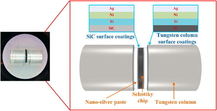
FIGURE 1. Photograph and the schematic of sintered SBD sample.
The Ag paste used in the experiment is NanoTach-X paste purchased from Tianjin polytechnic university. To lay the foundation for the subsequent exploration of the silver paste sintering process, some nessesarry characterization and testing experiments are conducted on the silver paste, such as thermal gravimetric analysis (TGA) and differential scanning calorimetry (DSC) tests. The steps of the pressureless sintering method used in this experiment are as follows (Figure 2A): first, dispensing the silver paste to the upper surface of the tungsten electrode column, then place the Schottky chip face up on the tungsten electrode after dispensing, and then dispensing silver paste to the front of the Schottky chip, and finally place another tungsten electrode column above the chip. After assembly, it is placed in a dedicated sintering equipment for sintering. As shown in Figure 2B, the sintering process includes three steps: pre-heating, sintering, and cooling. No additional pressure is applied throughout the sintering process to prevent the unwanted damage to the upper surface of schottky chips and the further electrical performance failure of the SBD.
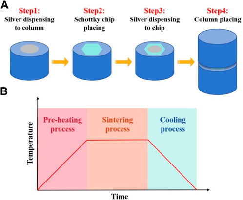
FIGURE 2. Schematic of the pressureless silver sintering process: (A) schematic of silver paste dispensing and device assembly; (B) schematic of sintering process curve.
The cross-section morphology of the joint was observed by scanning electron microscopy (SEM, ZEISS-SUPRA55) and the porosity of the joint was calculated by ImageJ software. Shear tests (DAGE-4000PXY) were performed under the crosshead speed of 0.2 mm/s to evaluate the joint strength, and the fracture surface feature of the sintered joint was also characterized by SEM. Besides, the ultimate reliability assessment testing mainly included the temperature cycling test, second sintering test, steady-state lifetime test, and intermittent lifetime test. Temperature cycling test means performing −65–175°C temperature cycles on the SBD sample. The second sintering samples were obtained after 500°C and 600°C temperature second sintering. The steady state life span test means exposing the SBD to the environment of 85°C for 1,000 h; and the intermittent life span test means performing 6,000 power on/off cycles on the SBD at 85°C temperature.
3 Results and discussion
According to the TGA and DSC curves as shown in Figure 3A, the weight content of terpilenol in silvepaste is 11.59% and it can be effectively volatilized at the temperature of 250°C. Due to the accumulating effect of nanoparticles, the micromorphology of the silver paste consisted of flaky particles with an average size of 1.43 um, as illustrated in Figures 3B, C.
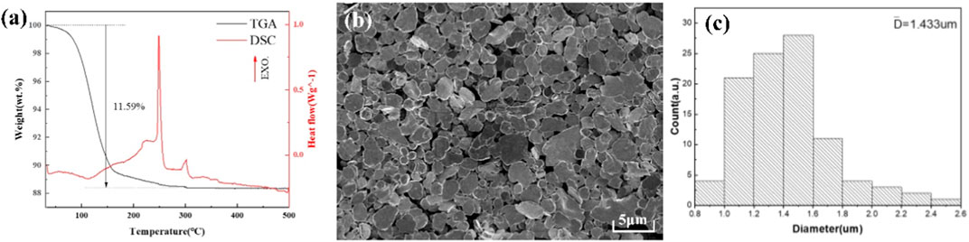
FIGURE 3. Characterization of the silver paste: (A) TGA and DSC curves of the silver paste; (B) SEM images of the silver paste; (C) size distribution of the silver paste particles.
For pressureless sintering, a pre selected parameters combination of 290°C/30 min based on the literature and the characteristics of the silver paste were utilized to examine the viability of the selected silver paste in connecting schottky chips and tungsten electrode columns.
SEM image in Figure 4A shows the typical microstructure of the silver sintered joint. Metallurgical bonding could be observed between the schottky chip and tungsten electrode column, and the thickness of the effective sintered layer was uniform. According to the magnification image in Figure 4B, the sintered silver paste showed the porous structure and the Ti/Ni/Ag metalization coatings remained stable. After calculation, the porosity of this joint was 14.1% and the shear strength was 34.3 MPa, indicating the feasibility of selected silver paste and pressureless sintering method.
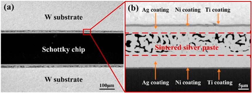
FIGURE 4. Cross-section morphologies of the sintered joint: (A) image at ×200 magnification; (B) image at ×5,000 magnification.
Figure 5 illustrates the effect of sintering temperature on the joint porosity and shear strength. The cross-sections of all samples sintered at different temperatures revealed a porous structure, however the porosity was highly dependent on the sintering temperature. With the temperature rising from 230°C to 290°C, the bonding area of the sintered Ag layer and Ag coating gradually increased. Three distinct sections of the sintered layer were chosen for the porosity calculation, which revealed a decreasing trend from 25.8% to 11.7%. At low temperatures, the organic components of the silver paste could not be completely removed and the structure was amorphous. Due to the low activation energy, surface diffusion was the predominant diffusion mode at lower temperatures. When the temperature rised, the complete volatilization of organic dispersant led to the densification of silver layer. Besides, the atom diffusion mechanism changed to grain boundary diffusion, which could improve the density of sintered layer as well. Shear strength was influenced by the joint porosity, which reached 35.2 MPa with the lowest porosity of 11.7% at 290°C. However, the considerable heat input resulting from the high temperature may be detrimental to the quality of the joint. Some researchers have claimed that a higher temperature (>290°C) will lead to the oxidation of substrate and silver joint, which decreased the shear strength and joint stability (Chua and Siow, 2016). Therefore, we chose 290°C as the optimal sintering temperature in our testing.
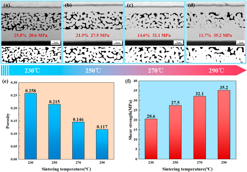
FIGURE 5. Morphorlogies and properties of the sintered joints at different temperatures with 30 min residence time: (A–D) cross-sections at 230°C–290°C; (E) porosities at 230°C–290°C; (F) shear strengths at 230°C–290°C.
The morphologies of sintered layers with varying residence times are depicted in Figure 6 a through d at the sintering temperature of 290°C. With the residence time increasing from 20 min to 50 min, the porosity droped from 19.4% to 8.7% for the growing of Ag particles, as shown in Figure 6E. However, the shear strength showed a trend of first rising and then falling, which can be found in Figure 6F. At the range of 20–40 min, the shear strength rised for the density increasing and reached the highest of 39.6 MPa with 40 min residence time, which has exceeded the shearing strength level of Au80Sn20 alloy soldering SBD joint (30 MPa). When the residence time further increased, the shear strength reduced to 36.5 MPa because of the coarsening effect of Ag grains. Therefore, 40 min was chosen as the optimal residence time for sintering.
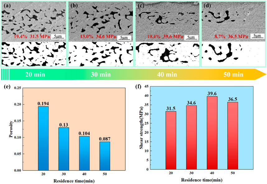
FIGURE 6. Morphorlogies and properties of the sintered joints at different residence time at 290°C sintering temperature: (A–D) cross-sections with 20–50 min; (E) porosities with 20–50 min; (F) shear strengths with 20–50 min.
The fracture surface morphology is shown in Figure 7A–C to investigate the fracture behavior of the sintered joint. For the 290°C/40 min sintered sample after shear test, a large number of shearing dimples could be observed, indicating the fracture occurred inside the sintered silver layer because the bonding strength of the sintered silver layer was superior to the bonding strength between sintered silver layer and Ag coatings. The sintering neck was thick and dense, showing the excellent bonding effect under this parameter.
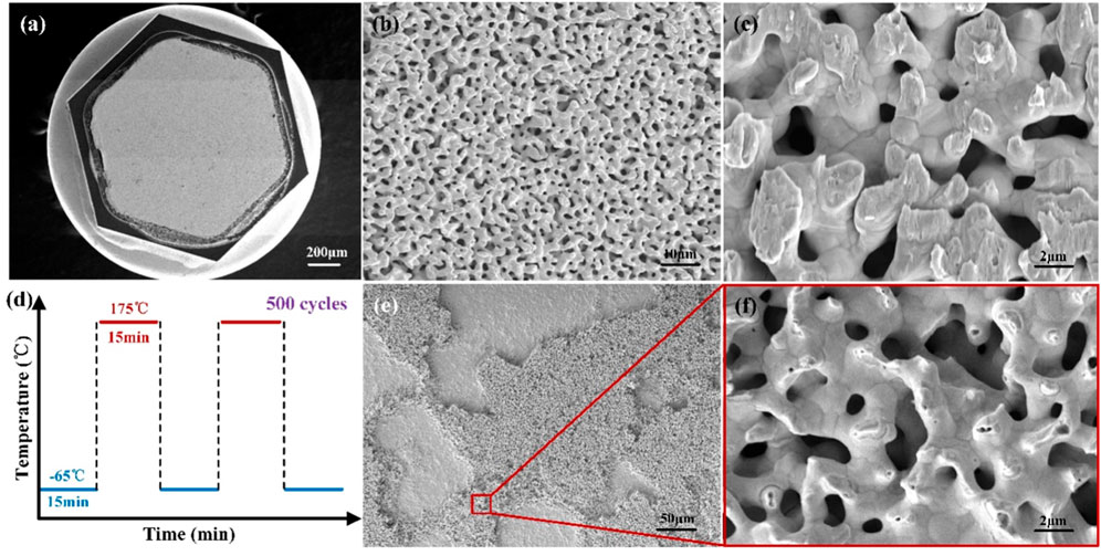
FIGURE 7. Fracture morphorlogy and temperature cycle test results: (A–C) fracture surface of the sintered joint; (D) temperature cycling curve; (E) fracture surface after temperature cycle test; (F) magnification of (E).
To meet the demand of extreme temperature resistance of SBD, temperature cycling test was conducted to evaluate the high and low temperature reliability. Figure 6D exhibits the temperature cycling test conditions in detail. A complete temperature cycle consisted of a low temperature period at −65°C for 15 min and a high temperature period at 175°C for 15 min. The heating time and cooling time were both 30 s. After 500 temperature cycles, a shear test was performed on the sintered silver joint and the fracture surface was observed. The joint strength after temperature cycling test was 37.9 MPa, reaching 95.7% of the sintered joint, indicating the silver joint had great temperature cycling resistance. Based on the fracture surfaces of Figures 7E, F, the fracture occurred mostly between the sintered silver layer and the Ag metalization coating, and the sintering neck was narrower than in Figure 7C, indicating that the pores in the Ag layer were larger. In addition, no dimples in the shearing direction were observed indicating that the sample’s flexibility decreased during temperature cycling. The thermal stress was caused by the differential in thermal expansion coefficients between sintered Ag, schottky chip, and W substrate. The pores in the sintered layer developed and accumulated, causing the joint to become brittle and lose strength.
Simulation with finite elements was utilized to assess the stress distribution of the temperature-cycling sample more precisely. Abaqus software was used to construct a finite element simulation model and emphasize the silver sintered layer, as illustrated in Figure 8A. Table 1 lists the material parameters of the sintered layer-Schottky chip and the W substrate. Due to the influence of porosity structure on the material characteristics, the silver sintered layer lacked pores. Two temperature cycles were included to the simulation model and the thermal state was identical to that of the temperature cycling test.
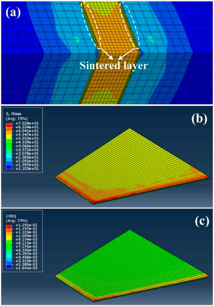
FIGURE 8. Simulation results of the temperature cycling sample: (A) simulation model; (B, C) equivalent stress and creep results.
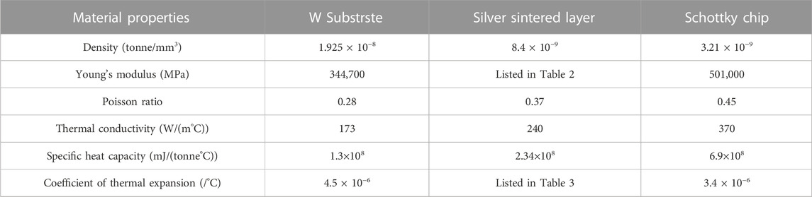
TABLE 1. Material properties of the simulation model.
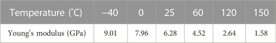
TABLE 2. Young’s modulus of sintered Ag layer at different temperatures.

TABLE 3. Coefficient of thermal expansion of sintered Ag layer at different temperatures.
The equivalent stress and creep cloud maps are illustrated in Figures 8B, C. At the edge of sintered Ag layer which contacted with the schottky chip and W substrate, the stress and creep concentration phenomenon could be found. Under the temperature cycling situation, these edges were more prone to cracking and became the weakest and most vulnerable areas, which was consistent with the experimental result that broke between the sintered silver layer and Ag coating.
In addition to the temperature cycling test, further stringent reliability tests were conducted to determine the quality of the sintered joint of SBD. To evaluate the high-temperature resistance of the sintered sample, second sintering test was performed at the temperatures of 500°C and 600°C, respectively. The shearing strength of the second sintered samples were 39.2 and 38.9 MPa, which were basically the same as the sintered sample, indicating the joint had great capablity of withstanding second high temperature processing, as illustrated in Table 4. A large number of sintering necks were pulled out according to Figure 9A, showing the fracture location were still inside the sintered layer. To determine the long-term dependability of silver sintered joints, a 1,000 h steady-state lifespan test was conducted at 85 °C under rigorous conditions. The shearing strength of the joint after test was 38.6 MPa, which was only 1 MPa less than the joint before this test. As shown in Figure 9B, some fracture sections were lack of sintering necks, indicating the fracture occurred at the bonding area between sintered layer and Ag coating. Due to the thinner sintering necks, tested joint strength was slightly lower than that of the sintered joint. Intermittent lifetime test was also performed to evaluate the joint reliability under cyclic electric stress. The tested sample was connected to the specific circuit system and was applied by periodic electric stress. One cycle included 3 min of power on time and 3 min of power off time. After 6,000 cycles at 85°C temperature, the joint strength was still 38.3 MPa, reaching 96.7% of the sintered joint. As demonstrated by the morphologies in Figure 9C, the thinning of sintering necks and the disappearance of shearing features on fractured sintering necks led to a reduction in strength, which was comparable to the results of a steady-state lifespan test.
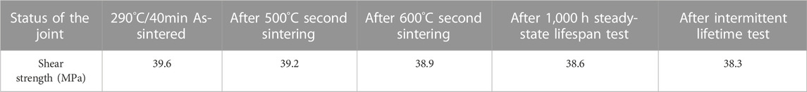
TABLE 4. Comparison of shear strengths before and after stringent reliability tests.
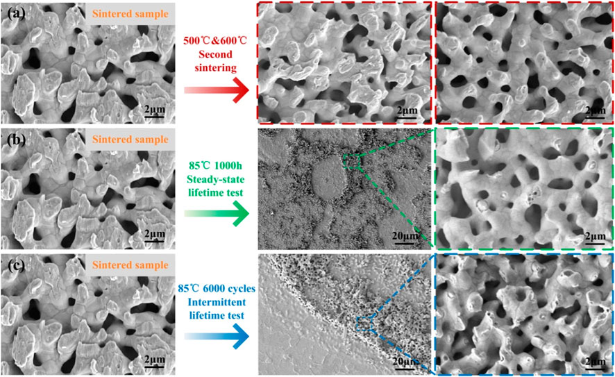
FIGURE 9. Results of the reliability test and the comparation of sintered sample: (A) second sintering; (B) steady-state lifetime test; (C) intermittent lifetime test.
4 Conclusion
In this paper, a high-quality silver joint is used for resistance to high temperatures. The pressureless sintering method was used to create schottky barrier diodes. Temperature and residence time during sintering were two major parameters that influenced the porosity and shear strength of joints. Under the optimal conditions of 290°C and 40 min, a porosity of 10.6% and a shear strength of 39.6% were produced. The sintered joint performed exceptionally well in mechanical/thermal/electrical testing, including the temperature cycling test, the second sintering test, the steady-state lifetime test, and the intermittent lifetime test. This study demonstrated the viability of pressureless sintering of silver joints with good high-temperature reliability, which has significant application potential in aeronautical SBD and other power electronics such as MOSFET and IGBT.
Data availability statement
The raw data supporting the conclusion of this article will be made available by the authors, without undue reservation.
Author contributions
CD: Investigation, Writing–review and editing. YW: Writing–original draft. PL: Supervision, Writing–review and editing. ZH: Writing–original draft. CW: Data curation, Writing–review and editing. XF: Conceptualization, Formal Analysis, Writing–review and editing. XL: Formal Analysis, Writing–review and editing.
Funding
The author(s) declare that no financial support was received for the research, authorship, and/or publication of this article.
Conflict of interest
The authors declare that the research was conducted in the absence of any commercial or financial relationships that could be construed as a potential conflict of interest.
Publisher’s note
All claims expressed in this article are solely those of the authors and do not necessarily represent those of their affiliated organizations, or those of the publisher, the editors and the reviewers. Any product that may be evaluated in this article, or claim that may be made by its manufacturer, is not guaranteed or endorsed by the publisher.
References
Cheng, S., Huang, C. M., and Pecht, M. (2017). A review of lead-free solders for electronics applications. Microelectron. Reliab. 75, 77–95. doi:10.1016/j.microrel.2017.06.016
Chin, H. S., Cheong, K. Y., and Ismail, A. B. (2010). A review on die attach materials for SiC-based high-temperature power devices. Metallurgical Mater. Trans. B Process Metallurgy Mater. Process. Sci. 41, 824–832. doi:10.1007/s11663-010-9365-5
Chua, S. T., and Siow, K. S. (2016). Microstructural studies and bonding strength of pressureless sintered nano-silver joints on silver, direct bond copper (DBC) and copper substrates aged at 300 °C. J. Alloys Compd. 687, 486–498. doi:10.1016/j.jallcom.2016.06.132
El-Daly, A. A., and Hammad, A. E. (2012). Enhancement of creep resistance and thermal behavior of eutectic Sn-Cu lead-free solder alloy by Ag and In-additions. Mater Des. 40, 292–298. doi:10.1016/j.matdes.2012.04.007
Fu, S., Mei, Y., Lu, G. Q., Li, X., Chen, G., and Chen, X. (2014). Pressureless sintering of nanosilver paste at low temperature to join large area (≥100 mm2) power chips for electronic packaging. Mater Lett. 128, 42–45. doi:10.1016/j.matlet.2014.04.127
Hausner, S., Weis, S., Wielage, B., and Wagner, G. (2016). Low temperature joining of copper by Ag nanopaste: correlation of mechanical properties and process parameters. Weld. World 60, 1277–1286. doi:10.1007/s40194-016-0381-1
Hong, K. J., Jeong, T. S., and Youn, C. J. (2014). Photocurrent spectroscopic study of temperature-dependent photoresponse and valence-band splitting in MnAl2S4 layers. J. Electron Mater 43, 3092–3097. doi:10.1007/s11664-014-3248-5
Igoshev, V. I., Kleiman, J. I., Shangguan, D., Wong, S., and Michon, U. Correction to: fracture of Sn-3.5%Ag solder alloy under creep, J. Electron. Mater., (2000), 29, 12, 1356-1361. doi:10.1007/s11664-000-0119-z
Igoshev, V. I., Kleiman, J. I., Shangguan, D., Wong, S., and Michon, U. (2018). Correction to: fracture of Sn-3.5%Ag solder alloy under creep. J. Electron Mater 47 (11), 6944. doi:10.1007/s11664-018-6588-8
Islam, M. N., Chan, Y. C., Rizvi, M. J., and Jillek, W. (2005). Investigations of interfacial reactions of Sn-Zn based and Sn-Ag-Cu lead-free solder alloys as replacement for Sn-Pb solder. J. Alloys Compd. 400, 136–144. doi:10.1016/j.jallcom.2005.03.053
Jiang, X., Zhai, D., Chen, J., Yuan, F., Li, Z., He, Z., et al. (2018). “Comparison study of surge current capability of body diode of SiC MOSFET and SiC Schottky diode,” in 2018 IEEE Energy Conversion Congress and Exposition (ECCE), Portland, OR, USA, 845–849. doi:10.1109/ECCE.2018.8558388
Li, R. Z., Hu, A., Bridges, D., Zhang, T., Oakes, K. D., Peng, R., et al. (2015). Robust Ag nanoplate ink for flexible electronics packaging. Nanoscale 7, 7368–7377. doi:10.1039/c5nr00312a
Maruyama, M., Matsubayashi, R., Iwakuro, H., Isoda, S., and Komatsu, T. (2008). Silver nanosintering: a lead-free alternative to soldering. Appl. Phys. A Mater Sci. Process 93, 467–470. doi:10.1007/s00339-008-4807-5
Mei, Y., Chen, G., Cao, Y., Li, X., Han, D., and Chen, X. (2013). Simplification of low-temperature sintering nanosilver for power electronics packaging. J. Electron Mater 42, 1209–1218. doi:10.1007/s11664-013-2561-8
Nandi, A., Rana, K. S., and Bag, A. (2021). Design and analysis of P-GaN/N-GaO based junction barrier Schottky diodes. IEEE Trans. Electron Devices 68, 6052–6058. doi:10.1109/TED.2021.3119261
Sakamoto, S., Sugahara, T., and Suganuma, K. (2013). Microstructural stability of Ag sinter joining in thermal cycling. J. Mater. Sci. Mater. Electron. 24, 1332–1340. doi:10.1007/s10854-012-0929-9
Satyanarayan, , and Prabhu, K. N. (2011). Reactive wetting, evolution of interfacial and bulk IMCs and their effect on mechanical properties of eutectic Sn-Cu solder alloy. Adv. Colloid Interface Sci. 166, 87–118. doi:10.1016/j.cis.2011.05.005
Tai, F., Guo, F., Xia, Z. D., Lei, Y. P., and Shi, Y. W. (2010). Effects of nano-structured particles on microstructure and microhardness of Sn-Ag solder alloy. J. Mater. Sci. Mater. Electron. 21, 702–707. doi:10.1007/s10854-009-9981-5
Tsao, L. C., and Chang, S. Y. (2010). Effects of Nano-TiO2 additions on thermal analysis, microstructure and tensile properties of Sn3.5Ag0.25Cu solder. Mater Des. 31, 990–993. doi:10.1016/j.matdes.2009.08.008
Wang, J., Chen, S., Zhang, L., Zhao, X., Duan, F., and Chen, H. (2021). Brief review of nanosilver sintering: manufacturing and reliability. J. Electron Mater 50, 5483–5498. doi:10.1007/s11664-021-09078-1
Wang, S., Ji, H., Li, M., and Wang, C. (2012). Fabrication of interconnects using pressureless low temperature sintered Ag nanoparticles. Mater Lett. 85, 61–63. doi:10.1016/j.matlet.2012.06.089
Wang, S., Li, M., Ji, H., and Wang, C. (2013). Rapid pressureless low-temperature sintering of Ag nanoparticles for high-power density electronic packaging. Scr. Mater 69, 789–792. doi:10.1016/j.scriptamat.2013.08.031
Ying, S., Ma, Z., Zhou, Z., Tao, R., Yan, K., Xin, M., et al. (2020). Device based on polymer Schottky junctions and their applications: a review. IEEE Access 8, 189646–189660. doi:10.1109/ACCESS.2020.3030644
Zhang, W., Chen, J., Deng, Z., Liu, Z., Huang, Q., Guo, W., et al. (2019). The pressureless sintering of micron silver paste for electrical connections. J. Alloys Compd. 795, 163–167. doi:10.1016/j.jallcom.2019.04.270
Keywords: silver sintered joint, schottky barrier diode, pressureless method, high-reliability, temperature cycling
Citation: Dai C, Wang Y, Lin P, Hao Z, Wang C, Feng X and Liu X (2023) Achieving high-quality silver sintered joint for highly-reliable schottky barrier diodes via pressureless method. Front. Mater. 10:1297827. doi: 10.3389/fmats.2023.1297827
Received: 20 September 2023; Accepted: 23 October 2023;
Published: 06 November 2023.
Edited by:
Shang Wang, Harbin Institute of Technology, ChinaReviewed by:
Su Ding, Xidian University, ChinaLakshmi Narayanan Mosur Saravana Murthy, Intel, United States
Copyright © 2023 Dai, Wang, Lin, Hao, Wang, Feng and Liu. This is an open-access article distributed under the terms of the Creative Commons Attribution License (CC BY). The use, distribution or reproduction in other forums is permitted, provided the original author(s) and the copyright owner(s) are credited and that the original publication in this journal is cited, in accordance with accepted academic practice. No use, distribution or reproduction is permitted which does not comply with these terms.
*Correspondence: Pengrong Lin, MTg1MDA0Nzg3NTRAMTYzLmNvbQ==; Zilin Hao, MTc4NjMxMTA2NzBAMTYzLmNvbQ==