 H. X. Yin
 Zh. Wang
- Kunming Institute of Physics, Kunming, Yunnan, China
Over the past decade, InAs/InAsSb superlattices and their photodetectors have been widely studied due to their potential applications in high-performance infrared detectors. However, InAs/InAsSb superlattice-based infrared (IR) detectors suffer from a serious limitation of deficient light absorption and the corresponding low quantum efficiency (QE). Recently, InGaAs/InAsSb type-II strained layer superlattices have been reported to have the capability to enhance the absorption of infrared light. In this study, we present a detailed comparative analysis on the optical properties, electrical properties, and detector performance of InGaAs/InAsSb and InAs/InAsSb strained layer superlattices. With the introduction of Ga into the InAs layers, the light absorption coefficient is observed to increase from 2,247 cm−1 for InAs/InAsSb superlattices to 3,442 cm−1 for InGaAs/InAsSb superlattices at the typical mid-wave infrared wavelength of 4.7 μm. However, this increase in light absorption coefficient does not boost the QE of the InGaAs/InAsSb superlattice detectors. Instead, quantum efficiency decreases from 45% for InAs/InAsSb superlattice detectors to 27% for InGaAs/InAsSb superlattice detectors at 150 K. This degradation in quantum efficiency for InGaAs/InAsSb superlattice detectors is found to be mainly caused by their poorer electrical properties, e.g., electron mobility and minority carrier lifetime. Fundamentally, the poorer electrical properties and lower quantum efficiency of InGaAs/InAsSb superlattice detectors are mainly due to the higher defect density within the materials, which is evidenced by the study of cross-sectional electron backscattered diffraction in these superlattices.
Introduction
Over the years, cooled infrared (IR) detectors and their focal plane arrays (FPAs), such as HgCdTe and InSb, have been widely applied in various industry sectors, including night vision, surveillance, and astronomy study (Kinch et al., 2010). Although cooling enables these IR detectors to achieve superior device performance, it leads to increased size, weight, power consumption, and cost (SWaPC), which limits their applications—especially their commercial applications. Advances in research on IR applications propose more stringent requirements for future IR detectors to have a smaller SWaPC. Thus, it is essential to fabricate IR detectors that can operate at a high operating temperature (HOT). More recently, the strained layer superlattice (SL)-based nBn structure was proposed for making HOT IR detectors, especially mid-wave infrared (MWIR) detectors (Pour et al., 2011; Klipstein et al., 2013; Martyniuk and Rogalski, 2013; Soibel et al., 2014; Tian et al., 2014). Earlier studies on these SL-based nBn detectors mainly focused on InAs/GaSb (Chang and Esaki, 1980) and InAs/InGaSb (Mailhiot and Smith, 1989) SLs, which, however, showed low quantum efficiency (QE) due to their poor minority carrier lifetime. Later on, Ga-free InAs/InAsSb SLs were proposed to achieve a higher QE as a result of the longer minority carrier lifetime (Steenbergen et al., 2011; Olson et al., 2012; Höglund et al., 2014). However, these InAs/InAsSb SL-based detectors still suffer from the limitation of lower light absorption.
One of the approaches to enhance light absorption in InAs/InAsSb SLs is to incorporate Ga into the InAs layers of the SLs (Steenbergen et al., 2013). Ariyawansa et al. (2016) reported that the IR light absorption coefficient can be significantly increased by incorporating Ga into the InAs layers to form InGaAs/InAsSb ternary strained layer superlattices. The bandgap energy of the InGaAs/InAsSb SLS can be tuned by adjusting the structure of the superlattice, and a higher IR absorption coefficient with an increase of close to 30%–35% was experimentally observed due to the enhanced electron-hole wave-function overlap within the SLs (Ariyawansa et al., 2016). However, there is not much information regarding the impact of Ga incorporation in the InAs layers on the device performance of the IR detectors based on these ternary InGaAs/InAsSb SLs. In this study, we present comparative research on the impact of Ga incorporation on the performance of InAs/InAsSb SL-based IR detectors, especially on the QE and dark current density. It has been found that the incorporation of Ga into the InAs layers enhances the light absorption coefficient at a wavelength of 4.7 µm from 2,247 cm−1 to 3,442 cm−1. However, the InGaAs/InAsSb SL-based IR detectors only show a quantum efficiency of 27%, while the InAs/InAsSb SL-based IR detectors show a higher quantum efficiency of 45%. In addition, the InGaAs/InAsSb SL-based IR detectors present a larger dark current density of 1.5 × 10⁻⁴A/cm2, while the InAs/InAsSb SL-based IR detectors present a much lower dark current density of 1.5 × 10⁻⁶A/cm2. The detailed reasons for changes in the detectors’ QE and dark current density will be elaborated in subsequent sections.
Experimental details
Figure 1 shows the barrier-based structure of the MWIR InGaAs/InAsSb and InAs/InAsSb SL-based IR detectors discussed in this study. Both structures were grown on Si-doped GaSb substrates using a Riber MBE49 solid-source molecular beam epitaxy (MBE) reactor. After necessary deoxidation and the growth of a buffer layer, the barrier-based structures were grown according to the sample structure shown in Figure 1, including a 200 nm n-type In(Ga)As/InAsSb contact layer, a 3,000-nm-thick unintentionally doped In(Ga)As/InAsSb absorption layer, a 200-nm-thick unintentionally doped AlAs0.08Sb0.92 layer, and a 200 nm n-type In(Ga)As/InAsSb top contact layer. All the doped layers have a doping concentration of 2 × 1018 cm−3. Note that the structure and growth parameters were kept exactly the same for both samples, such as absorption layer thickness, doping concentration, and strain compensation, which allows for a fair comparison between the two samples.
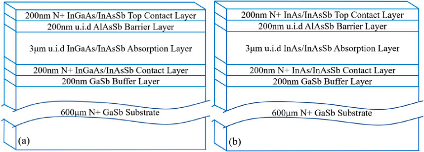
Figure 1. Schematic structures for (a) InGaAs/InAsSb and (b) InAs/InAsSb SL-based IR detectors.
The dark current of the single-pixel detectors fabricated from these samples was measured in a dewar with a vapor-cooled shield at different temperatures. The dewar was connected to a B1500A Semiconductor Parameter Analyzer to measure photocurrent under 150 K using a blackbody source. The responsivity and detectivity of the single-pixel detector were calculated from measurements taken with the blackbody source at 20 °C (293 K). The numerical aperture of the blackbody was 10 mm. No light filter was applied to control the photon flux. The detector noise was measured using a home-made noise characterization setup. Detailed measurements and calculation of responsivity, detectivity, and external quantum efficiency are provided in a later discussion.
Results and discussion
To understand the crystal lattice mismatching and crystal quality of the samples grown, XRD rocking curve measurements were conducted, the results of which are shown in Figure 2. It can be observed from the XRD results that the lattice mismatch in both the samples with InGaAs/InAsSb SLs and InAs/InAsSb SLs is less than 0.1%, allowing the growth of a thick absorption layer with high crystal quality. The full width at half-maximum intensity (FWHM) is observed to be 25 arcsec for InGaAs/InAsSb SLs, and their chemical composition is determined to be In0.806Ga0194As/InAs0.815Sb0.185. On the other hand, the XRD FWHM of InAs/InAsSb SLs is observed to be 20 arcsec, and their chemical composition is determined to be InAs/InAs0.65Sb0.35. The small XRD FWHM values for both samples indicate that both the InAs/InAsSb SL and InGaAs/InAsSb SL samples present excellent crystal quality and are suitable for fabricating IR detectors. It should be noted that the relatively larger XRD FWHM for the InGaAs/InAsSb SL sample could be attributed to the relatively higher defect density within, as discussed later.
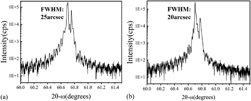
Figure 2. (004) XRD rocking curves (2θ-ω scan) for both the samples with InGaAs/InAsSb SLs (a) and InAs/InAsSb SLs (b).
To understand the bandgap and, thus, the cutoff wavelength of the InGaAs/InAsSb SLs and InAs/InAsSb SLs grown, optical absorption spectra were recorded at room temperature (RT) using a Nicolet FTIR Spectrometer (model iS50). Figure 3 shows the RT absorption spectra measured for InGaAs/InAsSb SL(a) and InAs/InAsSb SL(b) samples. It is observed that both the cutoff wavelength of the InAs/InAsSb SL and InGaAs/InAsSb SL samples are 4.7 μm. It should be noted that the cutoff wavelength refers to the point where the absorption is reduced to
where I is the actual light intensity, I0 is the total incident light intensity, and x is the thickness of the absorption material. Using Equation 1, the absorption coefficient at 4.7 μm is determined to be 3,442 cm−1 for InGaAs/InAsSb SLs and 2,247 cm−1 for InAs/InAsSb SLs, which agrees well with the results reported by Livneh et al. (2014). This confirms that the incorporation of Ga into InAs/InAsSb SLs enhances the light absorption coefficient of the SL materials and, thus, increases light absorption in the SLs when the absorption layer has the same thickness.
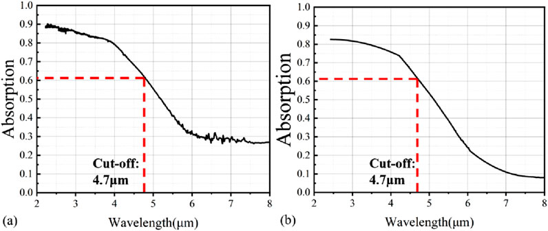
Figure 3. Room-temperature optical absorption spectra for the (a) InGaAs/InAsSb SL and (b) InAs/InAsSb SL samples.
To study the information of carrier mobility, temperature-dependent quantitative mobility spectrum analysis (QMSA) (Vurgaftman et al., 1999) was performed on the InAs/InAsSb SL- and InGaAs/InAsSb SL-based samples using a home-built Hall system with variable magnetic fields. Using the QMSA technique, the mobility signal from the SLs and that from GaSb substrates can be fitted and well-separated, and thus, in this study, only the data on SLs are presented and discussed as they correspond to this work. Figure 4 shows the sheet electron density and electron mobility of the InGaAs/InAsSb SLs and InAs/InAsSb SLs measured at different temperatures. As observed in Figure 4, the sheet electron density and electron mobility at 150 K were determined to be 9.24 × 1014 cm−2 and 7.08 × 102 cm2/(V·s) for InGaAs/InAsSb SLs and 4.02 × 1014 cm−2 and 4.43 × 103 cm2/(V·s) for InAs/InAsSb SLs, respectively. Figure 4 shows that the electron concentration of InGaAs/InAsSb SLs is approximately three times higher than that of InAs/InAsSb SLs at 150 K. As a result, the majority carrier mobility of InGaAs/InAsSb SLs is lower than that of InAs/InAsSb SLs on a similar scale.
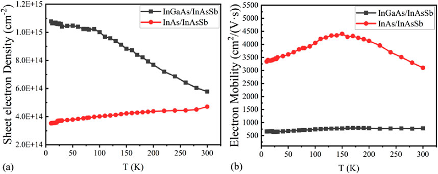
Figure 4. Temperature-dependent sheet electron carrier density (a) and electron mobility (b) in InGaAs/InAsSb and InAs/InAsSb SL samples measured using the QMSA technique.
As no proper equipment was available for this work to measure the minority carrier lifetime of InGaAs/InAsSb SLs and InAs/InAsSb SLs grown on GaSb substrates, diffusion length Lp was studied to extract the information of the minority carrier lifetime within. Notably, the diffusion length Lp can be described using Einstein’s relation, as shown in Equation 2 (Ferrari et al., 1985):
where μ is the carrier mobility and τ is the minority carrier lifetime. The information on minority carrier lifetime τ can be derived if the diffusion length Lp and carrier mobility μ are provided. To obtain the information on diffusion length Lp, SL detectors with various pixel sizes (360 μm, 180 μm, 120 μm, 60 μm, 30 μm, and 15 µm) were fabricated to study the change in photocurrent with pixel size. Figure 5 shows the schematic structure of the single-pixel detectors for measurement. The samples were etched to the barrier layer of AlAs0.08Sb0.92 after photolithography, forming single-pixel detectors with various pixel sizes. Metal electrodes were deposited on each pixel after surface passivation with an SiO2 layer.
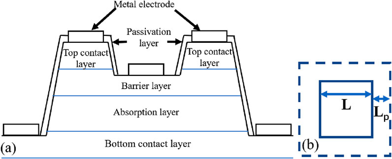
Figure 5. (a) Schematic structure of the SL detectors fabricated; (b) definition of the diffusion length.
Figure 6 shows the 150 K current–voltage (I–V) characteristics of the SL detectors with different pixel sizes of InGaAs/InAsSb (a) and InAs/InAsSb (b). In a unit device, the relationship between the photocurrent and size is provided in Equation 3:
where IL, Lp, and L are the photocurrent, the diffusion length, and the length of each side of the unit device, respectively (Klipstein et al., 2019). As the detectors were shallow etched in order to capture all photogenerated carriers within the region, the photocurrent density is assumed to be the same for the detectors with different pixel sizes under the same illumination and testing conditions. Thus, the diffusion length Lp can be calculated by changing the area of the unit device from L2 to (L+2Lp)2. Using Equation 3, the electron diffusion length at 150 K is derived to be 17.53 µm and 7.54 µm for InAs/InAsSb SLs and InGaAs/InAsSb SLs, respectively. With the electron diffusion length obtained and Einstein’s relation, the minority carrier lifetime is determined to be 130.7 ns and 120.9 ns for InAs/InAsSb SLs and InGaAs/InAsSb SLs, respectively. Compared to InAs/InAsSb SLs, the lower electron mobility and shorter minority carrier lifetime of InGaAs/InAsSb SLs well-explain the lower QE measured. The lower electron mobility and shorter minority carrier lifetime of InGaAs/InAsSb SLs might be related to defects caused by the Ga incorporation into the InAs layers, which are discussed in detail later in this work.
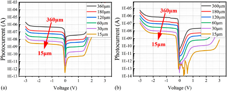
Figure 6. (a) 150 K I–V characteristics (photocurrent vs. bias) of InGaAs/InAsSb SL-based detectors with various pixel sizes; (b) 150 K I–V characteristics (photocurrent vs. bias) of InAs/InAsSb SL-based detectors with various pixel sizes for diffusion length calculation.
For IR detectors, responsivity R, detectivity D*, and external QE η are the most important figures of merit for evaluating device performance. To better understand their performance, these three parameters R, D*, and η were measured for detectors based on both InGaAs/InAsSb SLs and InAs/InAsSb SLs, and they were calculated using the following equations (Equations 4–6):
where Iph is the photocurrent and P is the incident light power.
where ∆f is the electrical bandwidth, S is the device active region area, and NEP is the noise equivalent power.
where Iph is the photocurrent, P is the illumination power, q is the electron charge, h is Planck’s constant, v is the light frequency, c is the speed of light in vacuum, and λ is the wavelength (Jone, 1959).
With the photocurrent shown in Figures 6A, B, the average detector’s QE at 150 K is determined to be ∼27% for an InGaAs/InAsSb SL-based detector with a pixel size of 15 µm and a bias of −0.5 V, while it is determined to be ∼45% for an InAs/InAsSb SL-based detector with a pixel size of 15 µm and a bias of −0.5 V. The average responsivity R is calculated to be 1.02 A/W for the InGaAs/InAsSb SL-based detector and 1.71 A/W for the InAs/InAsSb SL-based detector at 150 K, while the average detectivity D* is 4.59 × 10¹¹ (cm.Hz1/2)/W for the InGaAs/InAsSb SL-based detector and 8.22 × 10¹¹ (cm.Hz1/2)/W for the InAs/InAsSb SL-based detector at 150 K. As discussed previously, InGaAs/InAsSb SLs present an optical absorption coefficient higher than that of InAs/InAsSb SLs, and, thus, would be expected to exhibit a higher QE if the absorption layer thickness is similar. However, the measured QE of the InGaAs/InAsSb SL-based detector is much lower than that of the InAs/InAsSb SL-based detector. As QE of a photodetector is directly proportional to the carrier mobility and minority carrier lifetime of the absorber material in the IR detectors, the lower QE of the InGaAs/InAsSb SL-based detector can be mainly attributed to the lower carrier mobility and minority carrier lifetime in InGaAs/InAsSb SLs than those in InAs/InAsSb SLs, which is discussed later in this work. It should be noted that high defect density—and, thus, higher surface recombination in the InGaAs/InAsSb SL-based—could be another contributor contributing to the degradation of its photocurrent and, thus, its quantum efficiency. Further discussion of the defect density in the two samples is provided in later sections.
To further evaluate the device performance of these InAs/InAsSb SL- and InGaAs/InAsSb SL-based detectors, dark current measurements of these SL detectors under different temperatures were performed to assess the functionality. Figure 7 shows the temperature-dependent dark current measurements of the SL detectors with a pixel size of 15 µm. At ∼ 150 K (the targeted operating temperature for these SL-based detectors) and with a bias voltage of −0.5 V, the dark current density of the InAs/InAsSb SL-based detector is measured to be ∼1.5 × 10⁻⁶ A/cm2, while that of the InGaAs/InAsSb SL-based detector is ∼ 1.5 × 10⁻⁴ A/cm2. The InGaAs/InAsSb SL-based detector shows a dark current density that is 100 times higher than that of the InAs/InAsSb SL-based detector. Such a high dark current density might be related to the higher defect density in the InGaAs/InAsSb SLs, which is discussed in detail in a later section.
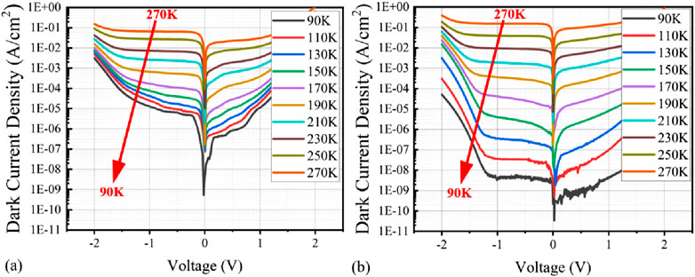
Figure 7. Temperature-relative dark current curves of the (a) InGaAs/InAsSb SL- and (b) InAs/InAsSb SL-based detectors with a pixel size of 15 µm.
To understand the dark current mechanism, Figure 8 shows an Arrhenius plot of the dark current density of the SL detectors with a pixel size of 15 μm under an applied bias voltage of −0.5 V. Usually, the dark current density presented in the Arrhenius plot can be fitted to determine defect activation energy, which is used to confirm the dominant mechanism of the dark current since it aligns closely with the theoretical analysis of temperature relation with different types of dark current, such as diffusion, Shockley–Read–Hall (SRH), and tunneling current reported in the literature (Ferrari et al., 1985). There are two distinct temperature regions observed for the InGaAs/InAsSb SL-based detector: (1) for the temperature range from 170 K to 270 K, the dark current density can be considered to be linearly correlated with temperature, as determined using the diffusion dark current equation
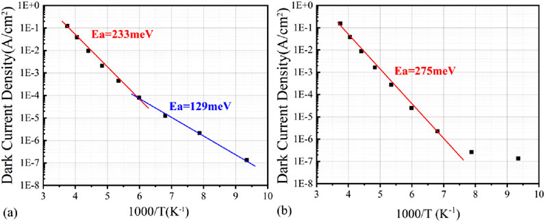
Figure 8. Arrhenius plot of the dark current density (ln|J| versus 1,000/T) under an applied bias of −0.5 V for (a) InGaAs/InAsSb SL- and (b) InAs/InAsSb SL-based detectors with a pixel size of 15 μm.
Similarly, there are also two distinct regions observed for the InAs/InAsSb SL-based detector: (1) for the temperature range from 150 K to 270 K, the dark current density can be considered to be linearly correlated with temperature, as determined using the diffusion dark current equation
To study and better understand the defects in the InAs/InAsSb SL and InGaAs/InAsSb SL samples, cross-sectional electron backscattered diffraction (EBSD) measurements were carried out to study the defects and their distribution across the SL structures. Figure 9 shows the cross-sectional EBSD maps for both InAs/InAsSb SL and InGaAs/InAsSb SL samples. Crystal lattice misorientation and, thus, defects are observed in both InAs/InAsSb SL and InGaAs/InAsSb SL samples (Zhu and De Graef, 2020). However, the crystal lattice misorientation in the InGaAs/InAsSb SL sample is observed to be much stronger than that in the InAs/InAsSb SL sample, which indicates that the InGaAs/InAsSb SL sample presents a defect density much higher than that of the InAs/InAsSb SL sample. Compared to the InAs/InAsSb SL sample, this higher defect density in the InGaAs/InAsSb SL sample well-explains its lower electron mobility and shorter minority carrier lifetime and, thus, its lower device performance, such as lower QE and higher dark current density, which were discussed in previous sections.
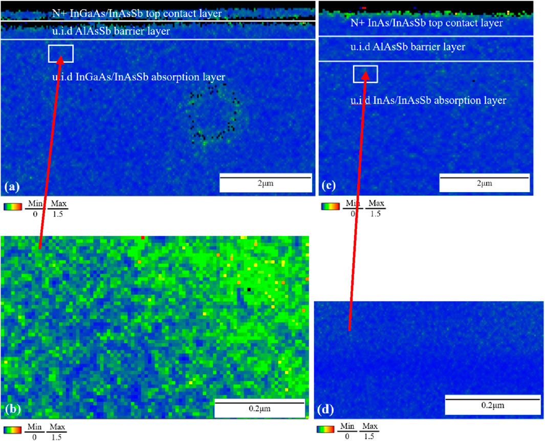
Figure 9. Cross-sectional EBSD maps of (a) the whole area of the InGaAs/InAsSb SL sample and (b) its magnified area; (c) the whole area of the InAs/InAsSb SL sample and (d) its magnified area.
Although detailed experimental analysis of these defects is beyond the scope of this work, first-principles calculations (Freysoldt et al., 2014) were used to study the formation energy of various possible defects in the InGaAs/InAsSb SL sample. The results of are presented in Table 1. It is observed that for InAsSb layers, the forming energy of Sb vacancy is the lowest (∼2.82 eV), which indicates that Sb vacancy will be the main type of defect in InAs/InAsSb SLs. However, the calculated forming energy for the GaSb-SbGa anti-site defect (∼1.71 eV) is much lower than that of Sb vacancy. This indicates that the incorporation of Ga into the InAs layer will generate GaSb-SbGa anti-site defects in the InGaAs/InAsSb SLs. In addition, it was reported that the relationship between the defect concentration and its forming energy can be described
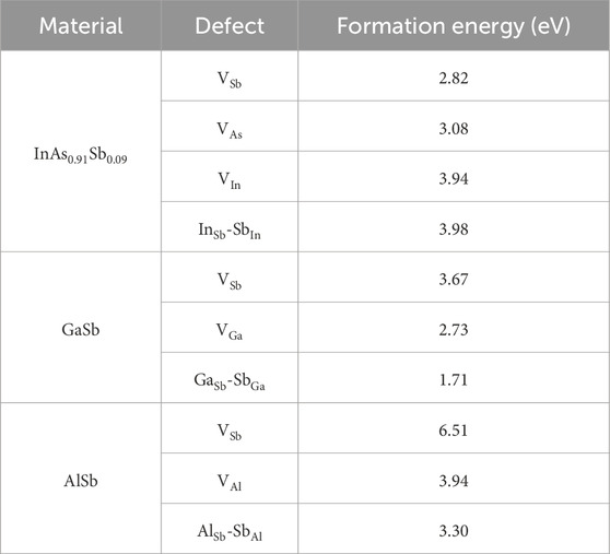
Table 1. Calculated forming energy for various possible types of defects in InAs/InAsSb and InGaAs/InAsSb SL structures.
Conclusion
In this study, we present a comparative research on InGaAs/InAsSb SLs and InAs/InAsSb SLs. It is found that the incorporation of Ga into InAs layers leads to the enhancement of the light absorption coefficient from 2,247 cm−1 to 3,442 cm−1 at a wavelength of 4.7 µm. However, this Ga incorporation also generates a lot of defects in the SL structures, which results in reduced electron mobility and shorter minority carrier lifetime; these effects seriously degrade the detector’s QE, reducing it from 45% for InAs/InAsSb SL-based detectors to 27% for InGaAs/InAsSb SL-based detectors. In addition, the higher defect density in InGaAs/InAsSb SLs also leads to significant SRH dark current below 167 K and, thus, a higher dark current density than that in InAs/InAsSb SL-based detectors. First-principles theoretical calculations suggest that the GaSb-SbGa anti-site defect is a likely potential defect type introduced by Ga incorporation due to its lower defect formation energy. This work contributes to a deeper understanding of InAs/InAsSb SL-based IR detectors.
Data availability statement
The raw data supporting the conclusions of this article will be made available by the authors, without undue reservation.
Author contributions
HY: Data curation, Formal analysis, Writing – original draft. ZW: Software, Writing – review and editing. JZ: Conceptualization, Writing – review and editing. ZJ: Resources, Writing – review and editing. CC: Investigation, Writing – review and editing. GD: Project administration, Writing – review and editing. XZ: Resources, Writing – review and editing. JY: Validation, Writing – review and editing. WL: Writing – review and editing, Data curation, Formal analysis, Investigation, Writing – original draft. RJ: Supervision, Writing – review and editing.
Funding
The author(s) declare that no financial support was received for the research and/or publication of this article.
Conflict of interest
The authors declare that the research was conducted in the absence of any commercial or financial relationships that could be construed as a potential conflict of interest.
Generative AI statement
The author(s) declare that no Generative AI was used in the creation of this manuscript.
Publisher’s note
All claims expressed in this article are solely those of the authors and do not necessarily represent those of their affiliated organizations, or those of the publisher, the editors and the reviewers. Any product that may be evaluated in this article, or claim that may be made by its manufacturer, is not guaranteed or endorsed by the publisher.
References
Ariyawansa, G., Reyner, C. J., Steenbergen, E. H., Duran, J. M., Reding, J. D., Scheihing, J. E., et al. (2016). InGaAs/InAsSb strained layer superlattices for mid-wave infrared detectors. Appl. Phys. Lett. 108, 022106. doi:10.1063/1.4939904
Baer, R. L. (2006). A model for dark current characterization and simulation. In: Proceedings Volume 6068, Sensors, Cameras, and Systems for Scientific/Industrial Applications VII. San Jose, California: Electronic Imaging. doi:10.1117/12.639844
Chang, L. L., and Esaki, L. (1980). Electronic properties of InAs-GaSb superlattices. Surf. Sci. 98, A288. doi:10.1016/0167-2584(80)90608-8
Ferrari, P. A., Goldstein, S., and Lebowitz, J. L. (1985). Diffusion, mobility and the Einstein relation. In: J. Fritz, A. Jaffe, and D. Szász, editors Statistical Physics and Dynamical Systems. Boston, MA: Birkhäuser, Vol. 10. p. 405–441.
Freysoldt, C., Grabowski, B., Hickel, T., Neugebauer, J., Kresse, G., Janotti, A., et al. (2014). First-principles calculations for point defects in solids. Rev. Mod. Phys. B 86, 253. doi:10.1103/RevModPhys.86.253
Fu, J., Guo, Z., Nie, C., Sun, F., Li, G., Feng, S., et al. (2024). Schottky infrared detectors with optically tunable barriers beyond the internal photoemission limit. Innovation 5, 100600. doi:10.1016/j.xinn.2024.100600
Höglund, L., Ting, D. Z., Soibel, A., Fisher, A., Khoshakhlagh, A., Hill, C. J., et al. (2014). Minority carrier lifetime in mid-wavelength infrared InAs/InAsSb superlattices: photon recycling and the role of radiative and Shockley-Read-Hall recombination mechanisms. Appl. Phys. Lett. 105, 193510. doi:10.1063/1.4902022
Jone, R. C. (1959). Quantum efficiency of detectors for visible and infrared radiation. Adv. Electron. Phys. 11, 87–183. doi:10.1016/s0065-2539(08)60994-4
Kinch, M. A., Schaake, H. F., Strong, R. L., Liao, P. K., Ohlson, M. J., Jacques, J., et al. (2010). High operating temperature MWIR detectors. Proc. SPIE 7660, 76602V. doi:10.1117/12.850965
Klipstein, P. C., Benny, Y., Gliksman, S., Glozman, A., Hojman, E., Klin, O., et al. (2019). Minority carrier lifetime and diffusion length in type II superlattice barrier devices. Infrared Phys. Technol. 96, 155–162. doi:10.1016/j.infrared.2018.11.022
Klipstein, P. C., Gross, Y., Aronov, D., ben Ezra, M., Berkowicz, E., Cohen, Y., et al. (2013). Low SWaP MWIR detector based on XBn focal plane array. Proc. SPIE 8704, 87041S. doi:10.1117/12.2015747
Livneh, Y., Klipstein, P. C., Klin, O., Snapi, N., Grossman, S., Glozman, A., et al. (2014). k.p model for the energy dispersions and absorption spectra of InAs/GaSb type-II superlattices. Phys. Rev. B 90, 039903. doi:10.1103/physrevb.90.039903
Mailhiot, C., and Smith, D. L. (1989). Long-wavelength infrared detectors based on strained InAs/Ga1-xInxSb type-II superlattices. J. Vac. Sci. Technol. A 7, 445–449. doi:10.1116/1.576201
Marozas, B. T., Hughes, W. D., Du, X., Sidor, D. E., Savich, G. R., and Wicks, G. W. (2018). Surface dark current mechanisms in III-V infrared photodetectors [Invited]. Opt. Mater. Express 8, 1419. doi:10.1364/ome.8.001419
Martyniuk, P., and Rogalski, A. (2013). HOT infrared photodetectors. Opto. Electron. Rev. 21, 239. doi:10.2478/s11772-013-0090-x
Olson, B. V., Shaner, E. A., Kim, J. K., Klem, J. F., Hawkins, S. D., Murray, L. M., et al. (2012). Time-resolved optical measurements of minority carrier recombination in a mid-wave infrared InAsSb alloy and InAs/InAsSb superlattice. Appl. Phys. Lett. 101, 092109. doi:10.1063/1.4749842
Pour, S. A., Huang, E. K., Chen, G., Haddadi, A., Nguyen, B. M., and Razeghi, M. (2011). High operating temperature midwave infrared photodiodes and focal plane arrays based on type-II InAs/GaSb superlattices. Appl. Phys. Lett. 98, 143501. doi:10.1063/1.3573867
Soibel, A., Hill, C. J., Keo, S. A., Hoglund, L., Rosenberg, R., Kowalczyk, R., et al. (2014). Room temperature performance of mid-wavelength infrared InAsSb nBn detectors. Appl. Phys. Lett. 105, 023512. doi:10.1063/1.4890465
Steenbergen, E. H., Cellek, O. O., Lui, S., Li, H., Shen, X., Smith, D. J., et al. (2013). The wonder of nanotechnology: quantum optoelectronic devices and applications. K. von Klitzing, M. Razeghi, and L. Esaki, editor Bellingham, WA: SPIE Press. p. 59.
Steenbergen, E. H., Connelly, B. C., Metcalfe, G. D., Shen, H., Wraback, M., Lubyshev, D., et al. (2011). Significantly improved minority carrier lifetime observed in a long-wavelength infrared III-V type-II superlattice comprised of InAs/InAsSb. Appl. Phys. Lett. 99, 251110. doi:10.1063/1.3671398
Tian, Z.-B., Godoy, S. E., Kim, H. S., Schuler-Sandy, T., Montoya, J. A., and Krishna, S. (2014). High operating temperature interband cascade focal plane arrays. Appl. Phys. Lett. 105, 051109. doi:10.1063/1.4892634
Vurgaftman, I., Meyer, J. R., Hoffman, C. A., Cho, S., Ketterson, J. B., Faraone, L., et al. (1999). Quantitative mobility spectrum analysis (QMSA) for hall characterization of electrons and holes in anisotropic bands. J. Electron. Mater. 28, 548–552. doi:10.1007/s11664-999-0110-2
Keywords: photodetectors, superlattices, InGaAs/InAsSb, InAs/InAsSb, defects
Citation: Yin HX, Wang Z, Zhang J, Jiang Z, Chang C, Deng GR, Zhou XC, Yang J, Lei W and Ji RB (2025) A comparative study of InGaAs/InAsSb and InAs/InAsSb strained layer superlattices. Front. Mater. 12:1633165. doi: 10.3389/fmats.2025.1633165
Received: 22 May 2025; Accepted: 23 June 2025;
Published: 29 July 2025.
Edited by:
Lu Wang, Soochow University, ChinaCopyright © 2025 Yin, Wang, Zhang, Jiang, Chang, Deng, Zhou, Yang, Lei and Ji. This is an open-access article distributed under the terms of the Creative Commons Attribution License (CC BY). The use, distribution or reproduction in other forums is permitted, provided the original author(s) and the copyright owner(s) are credited and that the original publication in this journal is cited, in accordance with accepted academic practice. No use, distribution or reproduction is permitted which does not comply with these terms.
*Correspondence: W. Lei, Y3psejEyOEAxNjMuY29t; R. B. Ji, amlyb25nYmluQDE2My5jb20=