 Wei Du1*†
 Quang M. Thai2†Jeremie Chrétien2Mathieu Bertrand3Lara Casiez3Yiyin Zhou4Joe Margetis5Nicolas Pauc2
 Alexei Chelnokov3
 Vincent Reboud3Vincent Calvo2John Tolle5Baohua Li6
 Shui-Qing Yu4*
- 1Department of Electrical Engineering and Physics, Wilkes University, Wilkes-Barre, PA, United States
- 2Univ. Grenoble Alpes, CEA, IRIG-DePhy, Grenoble, France
- 3Univ. Grenoble Alpes, CEA, LETI, Grenoble, France
- 4Department of Electrical Engineering, University of Arkansas, Fayetteville, AR, United States
- 5ASM, Phoenix, AZ, United States
- 6Arktonics, LLC, Fayetteville, AR, United States
A silicon-based monolithic laser has long been desired. Recent demonstration of lasing from direct bandgap group-IV alloy GeSn has opened up a completely new approach that is different from the traditional III-V integration on Si. In this study, high-quality GeSn samples were grown using a unique spontaneous Sn-enhanced growth recipe with an Sn composition as high as ~20.0%. GeSn lasers based on waveguide Fabry-Pérot and micro-disk cavities were fabricated and characterized. The waveguide features better local heat dissipation, while the micro-disk offers stronger optical confinement plus strain relaxation. The maximum operating temperature of 260 K was achieved from a waveguide laser, and a threshold of 108 kW/cm2 at 15 K was achieved from a micro-disk laser. A peak lasing wavelength of up to 3.5 μm was obtained with a 100-μm-wide ridge waveguide laser.
Introduction
Silicon, Germanium, and their alloys have been the most significant materials for the electronics industry that have driven the digital revolution. The well-known “Moore's law” has led to the rapid miniaturization of devices, which has yielded an ever-increasing density of fast components integrated on Si. Over the past few decades, the device feature size has almost reached to its ultimate physical limits. Meanwhile, a tremendous effort has been made to broaden the reach of these materials by developing their photonic functionalities, which is evidenced by the development of Si photonics [1]. Among the many active (light emitters, photodetectors, modulators, etc.) and passive (waveguides, couplers, switches, etc.) devices that make up a complete set of components for Si photonics, a light source that can be monolithically integrated on Si has long been desired for the next-generation photonic integrated circuits on an Si platform, but it is also the most challenging of these devices due to the intrinsic bandgap indirectness of group-IV semiconductors of Si, Ge, and SiGe alloys [2, 3]. Although Si-based rare-earth-doped lasers and Raman laser have been demonstrated [4–6], their low efficiency and lack of direct electrical pumping operation prevent them from being of practical use. A Ge laser relies on band-to-band transitions and employs strain-engineering and/or heavy n-type doping to compensate for the relatively small bandgap energy difference between its indirect and direct valleys. It therefore features a relatively high lasing threshold and suffers from fabrication difficulties [7, 8]. Currently, Si photonics utilizes direct bandgap III-V lasers as light sources via various integration approaches such as wafer-bonding or direct growth [9–11].
Recent study on GeSn alloys opens a new avenue for the development of Si-based optoelectronic devices with possible complementary metal-oxide-semiconductor (CMOS) compatibility [3]. By incorporating Sn into a Ge lattice, a new material platform, i.e., GeSn, has been created that has tremendous new electrical, optical, and mechanical properties that could dramatically change the future landscape of photonics [12, 13]. It has been predicted that the GeSn alloy could possess a direct bandgap if the Sn content is sufficient [14]. True direct bandgap GeSn was experimentally identified in 2014 [15], and this was followed by the first demonstration of an optically pumped GeSn band-to-band laser using a Fabry-Pérot (F-P) cavity in early 2015 [16]. Since then, GeSn lasing has been reported by various research groups worldwide [17–26]. To improve laser performance, various approaches have been applied to facilitate population inversion and carrier and optical confinement, such as using a heterostructure (HS), a multi-quantum-well (MQW) layer structure, or a micro-disk optical cavity. A brief review of GeSn laser development is shown in Table 1.
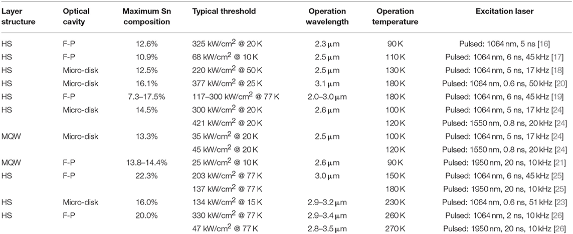
Table 1. A brief review of GeSn laser development.
Although the device performance has since been dramatically improved, as evidenced by the increased operation temperature and reduced lasing threshold, a study on laser configurations is highly desirable, as this could lead to further improvement of lasing in terms of possible room-temperature operation and electrical pumping. In this work, two GeSn samples with Sn compositions as high as ~20.0% were grown in a standard industrial reactor using newly developed growth recipes. Each sample was processed into both ridge waveguide and micro-disk structures. The former features better local heat dissipation, while the latter offers improved optical confinement and strain relaxation. The optically pumped lasing characteristics with the two structures were studied. The maximum operating temperature of 260 K was achieved for the ridge waveguide laser, with a lasing peak wavelength of up to 3.5 μm. Meanwhile, a 15 K threshold of 108 kW/cm2 was obtained for the micro-disk laser.
Material Growth and Characterization
The GeSn samples were grown on a Ge-buffered Si substrate using an industrial standard ASM Epsilon® 2000 PLUS reduced pressure chemical vapor deposition (RPCVD) reactor with commercially available precursors GeH4 and SnCl4. The Ge buffer layer is almost relaxed, with a nominal thickness of 700 nm (residual strain of ~−0.1%). A multiple-step Sn-enhanced growth recipe was used, which was developed and reported in our previous study on the spontaneous-relaxation-enhanced (SRE) Sn incorporation process: the gradual relaxation of the material facilitates Sn incorporation [17, 27], resulting in an increased Sn composition along the growth direction. Two samples (denoted by A and B) with Sn compositions as high as ~20.0% were grown. Detailed information on the growth process can be found elsewhere [28, 29]. After growth, the Sn composition was determined by secondary ion mass spectrometry (SIMS), strain was extracted by X-ray diffraction reciprocal space mapping (XRD RSM), and GeSn thickness and material quality were assessed through cross-sectional transmission electron microscopy (TEM). SIMS and XRD 2θ-ω scans were also used to cross-check the layer thicknesses and Sn compositions.
Figures 1a,b show cross-sectional views of TEM images of samples A and B, respectively. For each sample, the Ge/GeSn interface is clearly resolved, as marked with a dashed line. Two layers can be observed distinctly in the GeSn layer and are labeled 1st and 2nd in the images. The 1st layer over the Ge buffer is defective. This is due to the lattice mismatch between Ge and GeSn, which results in a relatively high threading dislocation density (TDD) [17]. The formation of threading dislocation loops in the 1st GeSn layer prevents the threading dislocations from penetrating the 1st GeSn layer and then propagating into the 2nd GeSn layer, resulting in a relatively low-defect density in the 2nd GeSn layer [30]. From TEM images, the thicknesses of the 1st and 2nd GeSn layers are 450 and 970 nm and 380 and 830 nm for samples A and B, respectively.
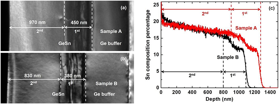
Figure 1. Cross-sectional TEM image of (a) sample A and (b) sample B showing each layer and the material quality; (c) SIMS depth profiles of the Sn concentration with the 1st and 2nd GeSn layers indicated.
The SIMS results for the GeSn are shown in Figure 1c. For each sample, two distinct layers can be clearly observed, corresponding to the 1st and 2nd GeSn layers seen in the TEM images. Both layers exhibit a spontaneously Sn-enhanced gradient. For sample A, the Sn composition increases from 11.0 to 15.0% in the 1st layer and from 15.0 to ~20.0% in the 2nd layer. Meanwhile, for sample B, the corresponding Sn composition increases are from 11.9 to 15.2% and from 15.2 to ~20.0%, respectively. The gradual increase in the Sn composition can be explained as follows: a nominal 11 or 11.9% Sn recipe was used at the beginning of material growth, and once the critical thickness of GeSn on Ge is reached, the relaxation of the GeSn could facilitate Sn incorporation, leading to an Sn increase along the growth direction.
To investigate the optical transitions in the GeSn layer, the PL spectra were studied using a 532-nm continuous wave (CW) laser as the excitation source and a standard off-axis configuration with a lock-in technique. A detailed description of the setup can be found elsewhere [15]. Figure 2A shows the normalized PL spectra of sample A measured at 300 K and 10 K. From 300 to 10 K, the integrated PL intensity increases ~50 times, as shown in Figure 2C, which is an unambiguous signature of a direct-bandgap material. A PL peak blueshift at lower temperature following the Varshni empirical model was observed as expected. Note that due to H2O and CH4 absorptions at 3.0 and 3.2 μm, a multi-peak feature was obtained in the shorter wavelength region of the main PL peak. Peaks at ~3,600 and 3,800 nm might be due to defects [31] and will be the subject of another study.
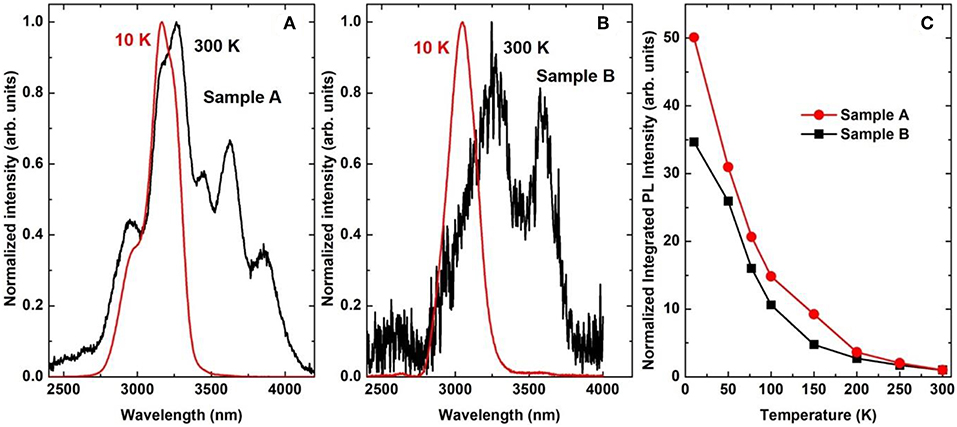
Figure 2. Normalized PL spectra at 10 and 300 K of (A) sample A and (B) sample B; (C) temperature-dependent normalized integrated PL intensity.
Normalized PL spectra of sample B as measured at 300 and 10 K are shown in Figure 2B. A PL peak intensity increase (of ~35 times, as shown in Figure 2C) together with a blue shift at lower wavelength were obtained. The PL peak of sample B at 10 K has a shorter wavelength than does sample A (3,050 nm vs. 3,150 nm), which is due to the higher compressive strain in the GeSn layer for sample B. The possible defect peak at ~3,600 nm was also observed for this sample.
Laser Device Fabrication
The GeSn samples were fabricated into laser devices. For each sample, two types of devices were fabricated. (i) Ridge-waveguide-based edge-emitting lasers, created using standard photolithography and wet chemical etching processes (devices A1 and B1 using samples A and B, respectively). The etching depth was set at 800 nm to provide sufficient mode confinement. After etching, the sample was lapped down to a ~70 μm thickness then cleaved to form the F-P cavity. (ii) Micro-disk surface-emitting lasers, created using e-beam lithography and anisotropic dry etching processes (devices A2 and B2). The under-etching in GeSn micro-disks is done via selective and isotropic CF4-based dry etching. The thickness and diameter of the micro-disk were measured to be ~1 and 10 μm, respectively. Scanning electron microscope (SEM) images of the devices are shown in the insets to Figure 3.
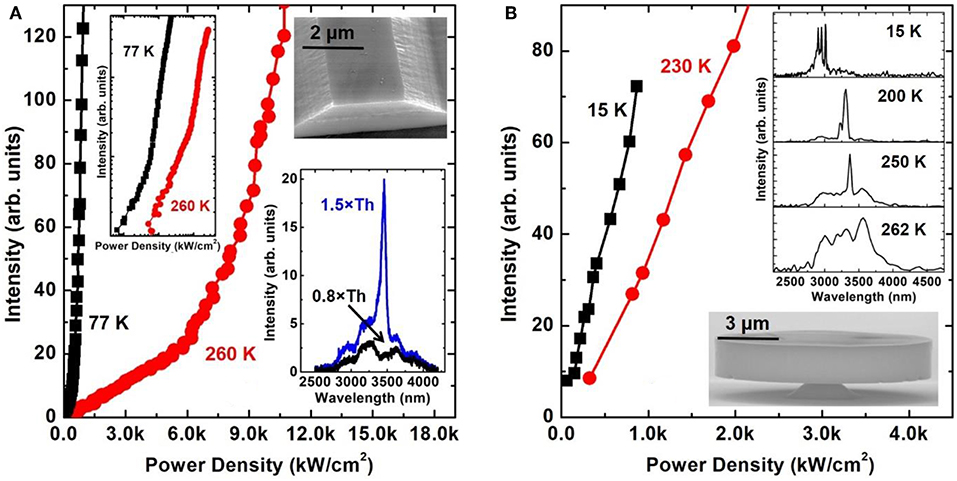
Figure 3. (A) Light output power vs. pump laser power of device A1 at 77 and 260 K. Inset: top left: L-L curves on a log-log scale; top right: SEM image of the device; bottom: emission spectra below (0.8×) and above (1.5×) the threshold at 260 K; (B) L-L curves of device A2 at 15 and 230 K. Inset: top: normalized emission spectra at different temperatures; bottom: SEM image of the device.
Optical Pumping Characterization
Optical pumping characterization of waveguide-based lasers was performed using a pulsed laser operating at 1,064 nm with a 45-kHz repetition rate and a 6-ns pulse width. The laser beam was collimated to a narrow stripe (~20 μm width) via a cylindrical lens to pump the GeSn waveguide structure. Since the spatial intensity profile of the laser beam has a Gaussian distribution, the knife-edge technique was applied to determine the pumping power density [32]. The device was first mounted on a Si chip carrier and then placed into a continuous flow cryostat for cryogenic characterization. The emission from the facet was collected by a spectrometer and then sent to an InSb detector (cutoff at 5.0 μm). The integrated emission intensity was measured by setting the grating at zero order.
Plots of the light output power vs. pump laser power for device A1 (width and length of 100 and 2,750 μm, respectively) at 77 and 260 K are shown in Figure 3A. The corresponding thresholds are 356 and 6,055 kW/cm2, respectively [26]. The maximum operating temperature of 260 K is close to room temperature. We attributed the relatively high operating temperature to (i) the high material quality achieved using our unique multiple-step Sn-enhanced growth recipe, evidenced by the low TDD; and (ii) the modal overlap of ~65.4% with the low TDD GeSn gain region (2nd GeSn layer) based on lasing mode pattern calculations using a 2D mode solver.
High-resolution lasing spectra were measured at 0.8 and 1.5 times the lasing threshold pumping power densities at 260 K and are shown in the inset in Figure 3A. Below- and above-threshold characteristics were clearly observed. A lasing peak at 3.5 μm was obtained. Due to the relatively large area of the cavity facet, the lasing spectra show typical multimode lasing characteristics [17]. The peak linewidth was extracted using a Gaussian data fitting method. In the inset to Figure 3A, the full width at half maximum (FWHM) of each resolved peak ranges from 2 to 3 meV [19]. The dramatic reduction in the peak linewidth compared with the FWHM of PL spectra measured at 10 K, which is ~23 meV (Figures 2A,B), is a clear lasing signature. Note that, based on theoretical calculations, the longitudinal mode spacing is ~1.3 nm while the transverse mode spacing is only ~0.01 nm. Due to the spectrometer limit of 0.1 nm, each observed peak should consist of multiple peaks that are mostly overlapping [16], and these peaks cannot be further discriminated.
The optical pumping characterization of micro-disk lasers was performed using a pulsed laser operating at 1,064 nm with a 51-kHz repetition rate and a 0.6-ns pulse width. The excitation laser beam was focused on the sample with a Cassegrain reflective objective, which was also used to collect the emission signal. The signal was then analyzed by a Fourier transform infrared (FTIR) spectrometer equipped with an InSb photodetector. The excitation spot has a ~20 μm diameter, which is large enough to cover the entire micro-disk cavity surface.
Figure 3B shows the L-L curves of device A2 at 15 and 230 K. The threshold at 15 K was measured to be 108 kW/cm2. The relatively low threshold is mainly due to the improved optical confinement offered by the micro-disk structure and the partial removal of the Ge/GeSn interface with the associated dislocations. At higher temperatures, due to the weak signal below the threshold, it is difficult to extract the threshold values accurately using only the L-L curves. However, the emission spectra below and above the threshold are very clear and so were used to identify the thresholds. The inset to Figure 3B shows the normalized emission spectra at different temperatures. The high-resolution spectrum at 15 K clearly indicates multimode lasing. A lasing peak can be observed up to 250 K. At 260 K, a broad emission spectrum with a lower intensity was obtained, suggesting that spontaneous light emission is dominant. As the temperature increases from 15 to 250 K, the corresponding lasing peak shifts from 2.9 to 3.4 μm.
Figure 4A shows the L-L curve of device B1 (width and length of 5 and 1,250 μm, respectively) at 77 and 150 K. The lasing thresholds varied from 203 to 609 kW/cm2 at temperatures ranging from 77 to 150 K, which is the maximum operating temperature. The lower threshold at 77 K of device B1 compared to device A1 might be due to the slightly higher Sn composition in sample B (Figure 1c), which results in a favorable population of electrons in the direct Γ valley under the same pumping power density [19]. On the other hand, the maximum operating temperature of device B1 (150 K) is substantially lower than that of device A1 (260 K). This can be explained by the wider ridge of device A1 (100 μm), which improves heat dissipation compared to device B1, which has a narrower ridge (5 μm) and suffers from enhanced free carrier absorption.
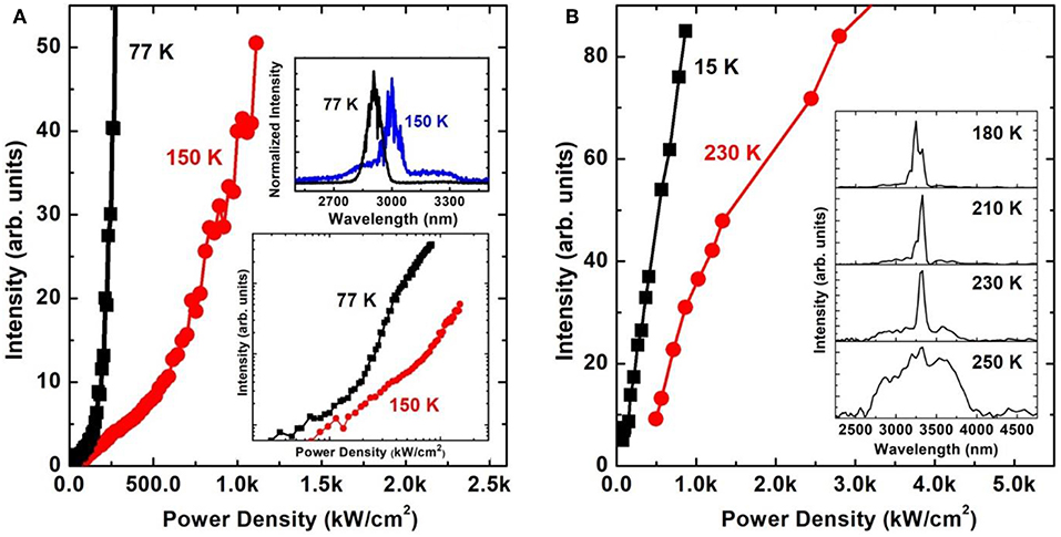
Figure 4. (A) Light output power vs. pump laser power of device B1 at 77 and 150 K. Inset: top: lasing spectra at 77 and 150 K; bottom: L-L curves on a log-log scale. (B) L-L curves of device B2 at 15 and 230 K. Inset: normalized emission spectra at different temperatures.
The inset to Figure 4A shows the lasing spectra at 1.5-times the lasing threshold at 77 and 150 K. A lasing peak redshift with increased temperature was observed, as expected. At 150 K, lasing occurred at 3.0 μm. Clear multimode lasing spectra can be seen at each temperature, with a peak linewidth that is similar to that of device A1.
The L-L curves of device B2 at 15 and 230 K are shown in Figure 4B. The threshold at 15 K was measured to be 177 kW/cm2, which is comparable to that of device B1. The normalized emission spectra at different temperatures are shown in the inset to Figure 4B. A maximum lasing operation temperature of 230 K was obtained, corresponding to a peak wavelength of 3.3 μm. The lasing characterization results are summarized in Table 2.
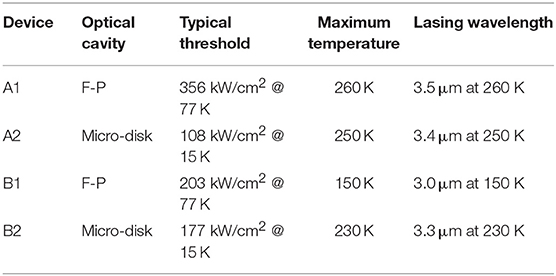
Table 2. Summary of lasing characterization.
Although the excitation methods are different for ridge waveguide and micro-disk lasers, a general discussion on device performance is as follows. (i) The material quality of sample A is higher than that of sample B, so that with the same laser structure, for the ridge waveguides (FP cavity), the maximum operating temperature of device A1 (260 K) is higher than that of device B1 (150 K); moreover, B1 has less efficient heat dissipation due to its narrow ridge width; for the micro-disks (MD), the maximum operating temperature of device A2 (250 K) is higher than that of device B2 (230 K), and, at 15 K, the threshold of A2 is lower than that of B2. (ii) Although sample B features slightly higher Sn content than sample A, the higher degree of compressive strain results in a similar lasing wavelength for all devices at the same temperature. (iii) Since the wider ridge waveguide structure features better local heat dissipation while the micro-disk structure offers improved optical confinement, they both achieve relatively high operating temperatures (260 and 250 K for samples A1 and A2). At higher temperature, local heating may be the dominant factor. (iv) For device B1, the heat dissipation capability is considerably reduced due to the narrow ridge width (5 μm compared to 100 μm in device A1); considering its weaker optical confinement compared with device B2, a maximum operating temperature of 150 K was obtained. Moreover, for device B2, the shorter pumping pulse duration (0.6 ns) reduces the local heating effect, resulting in its operating temperature being 80 K higher than that of device B1.
Conclusion
In this work, two GeSn samples were grown using a multiple-step Sn-enhanced growth approach and were then used to fabricate lasers with ridge waveguide and micro-disk structures. The enhanced heat dissipation and optical confinement improved the device performance. The maximum operating temperature of 260 K was achieved with a waveguide laser, and a threshold of 108 kW/cm2 at 15 K was obtained with a micro-disk laser. A lasing wavelength of up to 3.5 μm was observed. By optimizing the cavity geometry, further enhanced optical confinement and local heat dissipation can be achieved for FP and micro-disk cavities, respectively, and therefore the device performance can be significantly improved.
Data Availability Statement
The raw data supporting the conclusions of this manuscript will be made available by the authors, without undue reservation, to any qualified researcher.
Author Contributions
WD, NP, AC, VR, VC, BL, and S-QY proposed and guided the overall project. JM and JT conducted material growth and characterization. QT, JC, MB, LC, and YZ performed device fabrication and characterization.
Conflict of Interest
JM and JT were employed by the company ASM. BL was employed by the company Arktonics, LLC.
The remaining authors declare that the research was conducted in the absence of any commercial or financial relationships that could be construed as a potential conflict of interest.
Acknowledgments
The authors acknowledge financial support from the Air Force Office of Scientific Research under Grant Number FA9550-18-1-0045. WD appreciates support from the Provost's Research & Scholarship Fund at Wilkes University. The CEA team was supported by the French Elegante ANR and GeSn laser Carnot funding. The authors thank Dr. M. Benamara for his assistance in TEM imaging and Dr. A. Kuchuk at the Institute for Nanoscience & Engineering, University of Arkansas, USA, for his assistance in XRD measurement.
References
1. Soref R. The past, present, and future of silicon photonics. IEEE J Sel Top Quantum Elect. (2006) 12:1678–87. doi: 10.1109/JSTQE.2006.883151
2. Soref R. Mid-infrared photonics in silicon and germanium. Nat Photon. (2010) 4:495–7. doi: 10.1038/nphoton.2010.171
3. Soref R, Buca D, Yu SQ. Group IV photonics: driving integrated optoelectronics. Opt Photon News. (2016) 27:32–9. doi: 10.1364/OPN.27.1.000032
4. Bernhardi EH, van Wolferen HA, Agazzi L, Khan MR, Roeloffzen CG, Wörhoff K, et al. Ultra-narrow-linewidth, single-frequency distributed feedback waveguide laser in Al2O3:Er3+ on silicon. Opt Lett. (2010) 35:2394–6. doi: 10.1364/OL.35.002394
5. Bradley JD, Stoffer R, Agazzi L, Ay F, Wörhoff K, Pollnau M. Integrated Al2O3:Er3+ ring lasers on silicon with wide wavelength selectivity. Opt Lett. (2010) 35:73–5. doi: 10.1364/OL.35.000073
6. Rong H, Liu A, Jones R, Cohen O, Hak D, Nicolaescu R, et al. An all-silicon Raman laser. Nature. (2005) 433:292. doi: 10.1038/nature03273
7. Liu J, Sun X, Camacho-Aguilera R, Kimerling LC, Michel J. Ge-on-Si laser operating at room temperature. Opt Lett. (2010) 35:679–81. doi: 10.1364/OL.35.000679
8. Koerner R, Oehme M, Gollhofer M, Schmid M, Kostecki K, Bechler S, et al. Electrically pumped lasing from Ge Fabry-Perot resonators on Si. Opt Express. (2015) 23:14815–22. doi: 10.1364/OE.23.014815
9. Tanabe K, Watanabe K, Arakawa Y. III–V/Si hybrid photonic devices by direct fusion bonding. Sci Rep. (2012) 2:349. doi: 10.1038/srep00349
10. Liu H, Wang T, Jiang Q, Hogg R, Tutu F, Pozzi F, et al. Long-wavelength InAs/GaAs quantum-dot laser diode monolithically grown on Ge substrate. Nat Photonics. (2011) 5:416–9. doi: 10.1038/nphoton.2011.120
11. Chen S, Li W, Wu J, Jiang Q, Tang M, Shutts S, et al. Electrically pumped continuous-wave III–V quantum dot lasers on silicon. Nat Photonics. (2016) 10:307–11. doi: 10.1038/nphoton.2016.21
12. Ghetmiri SA, Du W, Benjamin Conley R, Mosleh A, Nazzal A, Richard Soref A, et al. Near and mid-infrared photoluminescence from Ge1-xSnx thin films on Si substrates. JVST B. (2014) 32:060601. doi: 10.1116/1.4897917
13. Tran H, Du W, Ghetmiri S, Aboozar Mosleh A, Sun G, Richard Soref A, et al. Systematic Study of Ge1-xSnx absorption coefficient and refractive index for the device applications of Si-based optoelectronics. J Appl Phys. (2016) 119:103106. doi: 10.1063/1.4943652
14. VD'Costa R, Fang Y, Tolle J, Kouvetakis J, Menéndez J. Ternary GeSiSn alloys: new opportunities for strain and band gap engineering using group-IV semiconductors. Thin Solid Films. (2010) 518:2531–7. doi: 10.1016/j.tsf.2009.09.149
15. Ghetmiri S, Du W, Margetis J, Mosleh A, Cousar L, Conley BR, et al. Direct-bandgap GeSn grown on silicon with 2230 nm photoluminescence. Appl Phys Lett. (2014) 105:151109. doi: 10.1063/1.4898597
16. Wirths S, Geiger R, von den Driesch N, Mussler G, Stoica T, Mantl S, et al. Lasing in direct-bandgap GeSn alloy grown on Si. Nat Photon. (2015) 9:88–92. doi: 10.1038/nphoton.2014.321
17. Al-Kabi S, Ghetmiri SA, Margetis J, Pham T, Zhou Y, Dou W, et al. An optically pumped 2.5 μm GeSn laser on Si operating at 110 K. Appl. Phys. Lett. (2016) 109:171105. doi: 10.1063/1.4966141
18. Stange D, Wirths S, Geiger R, Schulte-Braucks C, Marzban B, von den Driesch N, et al. Optically pumped GeSn microdisk lasers on Si. ACS Photonics. (2016) 3:1279–85. doi: 10.1021/acsphotonics.6b00258
19. Margetis J, Al-Kabi S, Du W, Dou W, Zhou Y, Pham T, et al. Si-based GeSn lasers with wavelength coverage of 2–3 μm and operating temperatures up to 180 K. ACS Photonics. (2018) 5:827–33. doi: 10.1021/acsphotonics.7b00938
20. Reboud V, Gassenq A, Pauc N, Aubin J, Milord L, Thai QM, et al. Optically pumped GeSn micro-disks with 16% Sn lasing at 3.1 μm up to 180 K. Appl Phys Lett. (2017) 111:092101. doi: 10.1063/1.5000353
21. Margetis J, Zhou Y, Dou W, Grant PC, Alharthi B, Du W, et al. All group-IV SiGeSn/GeSn/SiGeSn QW laser on Si operating up to 90 K. Appl Phys Lett. (2018) 113:221104. doi: 10.1063/1.5052563
22. von den Driesch N, Stange D, Rainko D, Povstugar I, Zaumseil P, Capellini G, et al. Advanced GeSn/SiGeSn group IV heterostructure lasers. Adv Sci. (2018) 5:1700955. doi: 10.1002/advs.201700955
23. Thai QM, Pauc N, Aubin J, Bertrand M, Chrétien J, Delaye V, et al. GeSn heterostructure micro-disk laser operating at 230 K. Opt Express. (2018) 26:32500–8. doi: 10.1364/OE.26.032500
24. Stange D, von den Driesch N, Zabel T, Armand-Pilon F, Rainko D, Marzban B, et al. GeSn/SiGeSn heterostructure and multi quantum well lasers. ACS Photonics. (2018) 5:4628–36. doi: 10.1021/acsphotonics.8b01116
25. Dou W, Zhou Y, Margetis J, Ghetmiri SA, Al-Kabi S, Du W, et al. Optically pumped lasing at 3 μm from compositionally graded GeSn with tin up to 22.3%. Opt Lett. (2018) 43:4558–61. doi: 10.1364/OL.43.004558
26. Zhou Y, Dou W, Du W, Ojo S, Tran H, Ghetmiri S, et al. Si-based GeSn lasers with ridge and planar waveguide structures and operating temperatures up to 270 K. ACS Photonics. (2017) 6:1434–41. doi: 10.1021/acsphotonics.9b00030
27. Aubin J, Hartmann JM, Gassenq A, Rouvière JL, Robin E, Delaye V, et al. Growth and structural properties of step-graded, high Sn content GeSn layers on Ge. Semicond Sci Technol. (2017) 32:094006. doi: 10.1088/1361-6641/aa8084
28. Margetis J, Ghetmiri SA, Du W, Conley BR, Mosley A, Soref R, et al. Growth and characterization of epitaxial Ge1-xSnx alloys and heterostructures using a commercial CVD system. ECS Trans. (2014) 64:711–20. doi: 10.1149/06406.0711ecst
29. Margetis J, Yu S-Q, Bhargava N, Li B, Du W, Tolle J. Strain engineering in epitaxial Ge1–xSnx: a path towards low-defect and high Sn-content layers. Semicond Sci Technol. (2017) 32:124006. doi: 10.1088/1361-6641/aa7fc7
30. Dou W, Benamara M, Mosleh A, Margetis J, Grant P, Zhou Y, et al. Investigation of GeSn strain relaxation and spontaneous composition gradient for low-defect and high-Sn alloy growth. Sci Rep. (2018) 8:5640. doi: 10.1038/s41598-018-24018-6
31. Tonkikh AA, Eisenschmidt C, Talalaev VG, Zakharov ND, Schilling J, Schmidt G, et al. Pseudomorphic GeSn/Ge (001) quantum wells: examining indirect band gap bowing. Appl Phys Lett. (2013) 103:032106. doi: 10.1063/1.4813913
Keywords: GeSn, laser, mid-infrared, micro-disk, ridge waveguide
Citation: Du W, Thai QM, Chrétien J, Bertrand M, Casiez L, Zhou Y, Margetis J, Pauc N, Chelnokov A, Reboud V, Calvo V, Tolle J, Li B and Yu S-Q (2019) Study of Si-Based GeSn Optically Pumped Lasers With Micro-Disk and Ridge Waveguide Structures. Front. Phys. 7:147. doi: 10.3389/fphy.2019.00147
Received: 20 June 2019; Accepted: 19 September 2019;
Published: 14 October 2019.
Edited by:
Shinichi Saito, University of Southampton, United KingdomReviewed by:
Dan Buca, Julich Research Centre, GermanyHuiyun Liu, University College London, United Kingdom
Copyright © 2019 Du, Thai, Chrétien, Bertrand, Casiez, Zhou, Margetis, Pauc, Chelnokov, Reboud, Calvo, Tolle, Li and Yu. This is an open-access article distributed under the terms of the Creative Commons Attribution License (CC BY). The use, distribution or reproduction in other forums is permitted, provided the original author(s) and the copyright owner(s) are credited and that the original publication in this journal is cited, in accordance with accepted academic practice. No use, distribution or reproduction is permitted which does not comply with these terms.
*Correspondence: Wei Du, d2VpLmR1QHdpbGtlcy5lZHU=; Shui-Qing Yu, c3l1QHVhcmsuZWR1
†These authors have contributed equally to this work