 Mingyang Yang1
 Ming Zhou
- 1State Key Laboratory of Tribology, School of Mechanical Engineering, Tsinghua University, Beijing, China
- 2Key Laboratory for Advanced Materials Processing Technology, Ministry of Education, Beijing, China
In this paper, a similar Fabry-Perot cavity structure utilizing a multilayer film structure consisting of an ultrathin metal film is demonstrated for absorbing the infrared ray. This structure has low emissivity in the atmospheric window (3–5 and 8–14 μm) and high emissivity in the nonatmospheric window (5–8 μm). These properties improved the stealth performance which causes the high emissivity in 5–8 μm to radiate more energy to reduce its temperature. Based on this, the periodic microstructures were added to the surface of the materials that enhanced the absorption of terahertz wave (0.1–2.7 THz). The absorber based on multilayer film has a simple structure and low manufacturing cost. This work may provide a new strategy for infrared and terahertz compatible stealth technology.
Introduction
Materials with wavelength-selective absorption capacity have application potential in selective thermal radiation [1–6], thermal photovoltaic systems [7–12], infrared stealth [13–18], etc., which attracted the attention of many scholars. Radiation cooling is to achieve cooling effect by radiating its own heat to outer space in the form of electromagnetic waves. According to Kirchhoff’s law, the emissivity of an object is equal to its absorptivity in thermal equilibrium. To improve efficiency, the materials should have a high emissivity in 8–14 μm and have a low emissivity in nonatmospheric window to reduce the absorption of radiation from other objects in the environment. In the field of thermal photovoltaics, the spectral selective absorption coating is the core component, which directly determines the light-to-heat conversion efficiency of the entire system. The wavelength-selective absorber needs to have high emissivity in the visible-near infrared band (0.3–2.5 μm) and the lowest possible emissivity in the mid-and-far infrared band (2.5–25 μm), where the thermal radiation at its own working temperature is located. This property plays the role of restraining energy loss caused by radiation heat dissipation while absorbing the energy of sunlight.
In the field of infrared stealth, the performance requirements for wavelength-selective absorption materials are opposite to that of radiation cooling. The materials need to have low emissivity in the two atmospheric windows (3–5 and 8–14 μm) to reduce the possibility of being detected by the detection equipment. According to Stephen-Boltzmann’s law, the radiation energy of an object, defined as the radiant exitance W, W = εσT4, where σ is Stephen-Boltzmann’s constant and ε and T are the emissivity and absolute temperature of the object, respectively. Therefore, reducing object radiation can be achieved by cooling or reducing emissivity. The main means to achieve stealth is to reduce the emissivity which causes the cost of cooling to be high [19]. There is a serious problem that the low emissivity of the whole band will affect the heat exchange process, making it difficult for heat to diffuse out in time. This may cause heat accumulation and increase the temperature of the target, thus increasing the radiation energy of the object and weakening the stealth performance. Materials with wavelength-selective absorption capabilities also have great application potential in infrared stealth technology. Specifically, the material needs to have a low emissivity in 3–5 and 8–14 μm to reduce detectability, while having a high emissivity in 5–8 μm outside the atmospheric window, which can diffuse the heat in time and lower its temperature to realize better infrared stealth. Most of the existing materials do not have such characteristics, so it is difficult to achieve the selective absorption performance to meet the stealth requirement by using traditional material systems.
Metamaterials or photonic crystals can be used to modulate the spectral absorption characteristics [20–22], so they have application prospects in the field of wavelength-selective absorption. The existence of the photonic bandgap in the photonic crystal makes it attract attention, and its absorption spectrum can be controlled through structural design. Similarly, the plasmonic structure has attracted attention due to its excellent electromagnetic response performance [23–25] and usually consists of a top patterned metal layer, a middle dielectric spacer, and a reflective metal substrate. Adjusting the absorptivity of these structures is mainly through electromagnetic resonance, which can tune the resonant frequency according to the reasonable structure design and even expand or move the resonance region. Due to the high manufacturing cost and the difficulty in realizing the excitation of ultrawideband resonance mode, the practical application of these materials is still limited.
In recent years, the researches of metamaterial functional devices in the terahertz band have made great progress, such as terahertz perfect absorbers [26], filters [27], stealth devices [28–30], and EIT devices [31]. As the improvement of related research about terahertz radar, the development of stealth devices has received a lot of attention. The metamaterials currently used for stealth in the terahertz band are mainly designed through microstructures, utilizing subwavelength structure arrays to control conductivity and magnetic permeability, thereby generating strong absorption at specific frequencies. Because of the contradiction between terahertz and infrared stealth requirements for material (low reflection and high absorption in terahertz; high reflection and low absorption in infrared), there are many problems in stealth materials compatible with the two wavebands.
In this work, the radiation characteristics of ultrathin Pt layer and impedance matching were utilized to design a wavelength-selective absorber based on planarized platinum/silicon (Pt/Si) multilayer film for infrared stealth. This absorber can effectively suppress thermal radiation in two atmospheric windows and enhance thermal radiation in the nonatmospheric window. Meanwhile, the absorber has the advantages of simple structure and easy to mass manufacturing. The overall resonance frequency of the structure was tuned by changing the thickness of the film. Also, microstructures were added to the surface to meet the requirements to enhance the absorption of terahertz waves. This research may provide a new strategy for stealth materials compatible with infrared and terahertz.
Result and Discussion
The Wavelength-Selective Absorber in Infrared Band
The wavelength-selective absorber used for infrared stealth in 3–14 μm consists of four layers, including one ultrathin Pt layer, one bottom reflective Pt layer, and two Si dielectric spacers, shown in Figure 1A. For the unique radiation characteristics of metals, the ultrathin Pt layer plays an important role as the main radiation layer. The silicon used in this research is crystalline silicon. The two Si layers tuned the characteristics of wavelength-selective absorption through impedance matching. The thickness of each layer was calculated by COMSOL; finally, the whole structure met the requirements of infrared stealth, shown in Figure 1B. The absorber has low absorptivity in the two atmospheric windows (3–5 and 8–14 μm), and high absorptivity in the nonatmospheric window (5–8 μm). Meanwhile, the manufacturing method of the designed structure is relatively simple; large-scale manufacturing could be realized through electron beam evaporation and magnetron sputtering.
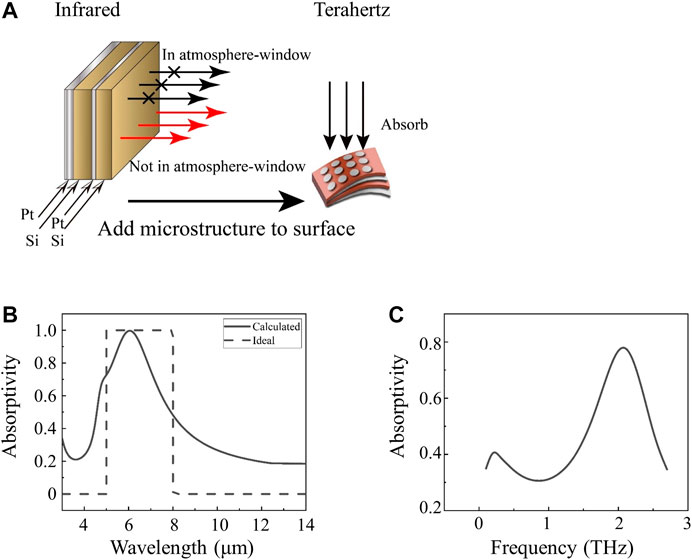
FIGURE 1. (A) Schematic of wavelength‐selective absorber in infrared and added microstructure in terahertz; (B) calculated and ideal absorptivity of the absorber in infrared; (C) absorptivity in terahertz (added microstructure).
The enhancement of thermal radiation in 5–8 μm is quite distinct from the traditional metal-based absorber (plasmonic resonance in metamaterials); this work utilized the radiation characteristics of the ultrathin Pt layer. The Pt has a large extinction coefficient and a high density of free electrons in the infrared band. Because the ultrathin Pt layer cannot shield the fluctuating current from radiating to free space due to the tunneling effect, this layer has a higher absorptivity in the infrared band [32]. But the bulk metal can screen the fluctuating current, so the bottom Pt layer played a role in reflecting the infrared wave. Therefore, the ultrathin Pt layer is essential for increasing the absorptivity.
However, a single ultrathin Pt layer cannot achieve the requirements of wavelength-selective absorption in the infrared band. The overall absorption characteristics are adjusted through the dielectric Si to meet the design requirements. In this work, the root-mean-square deviation (RMSD) is used for quantification of the wavelength-selective absorptivity between the calculated and ideal absorber as Eq. 1.
where εcal,λ and εideal,λ are the absorptivity of calculated and ideal absorber within 3–14 μm and N is the number of wavelengths.
The thickness of the top and middle Si layers was obtained when the value of RMSD between calculated and ideal absorber reached the minimum as shown in Figure 2.
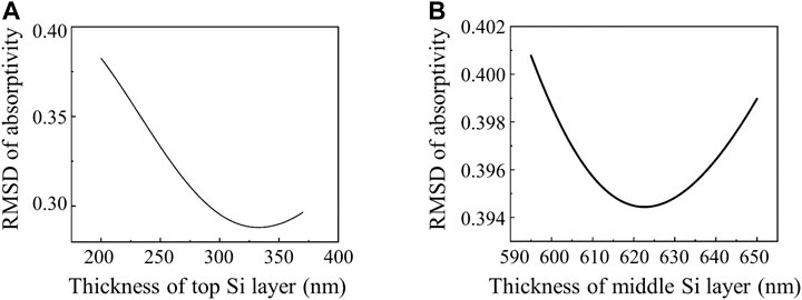
FIGURE 2. Root‐mean‐square deviation (RMSD) of the absorptivity relative to the ideal absorber with thickness changes. (A) in the top Si spacer; (B) in the middle Si space.
The wavelength-selective absorptivity requirements of infrared stealth could be met when the top Si layer is 333 nm and the middle Si layer is 623 nm. Because the bottom Pt layer is used for reflecting the infrared wave, the thickness should not be less than 50 nm. In this research, the thickness of the bottom Pt layer is 100 nm. Meanwhile, the ultrathin Pt layer is 15 nm, considering the film-forming property and the radiation performance. The absorptivity of the material was shown in Figure 1B. Based on the impedance matching principle, the addition of Si dielectric spacer adjusted the wavelength-selective absorptivity. Within a certain spectral range, the impedance of a structure matches the impedance of air (the real part of impedance close to 1 and imaginary part close to 0); the incident electromagnetic waves can enter the structure instead of being reflected on the surface. The impedance can be calculated by Eq. 2.
where S11 and S21 are the S-parameters of the wavelength-selective absorber. The results showed that the similarity of the impedance of absorber to the impedance of air (quantified by RMSD) in the high absorptivity region (5–8 μm) is 1.6 + 0.9i, while the value of the similarity in atmospheric windows is 3.01 + 3.06i (3–5 μm) and 1.38 + 2.26i (8–14 μm). The calculation results are shown in Figure 3.
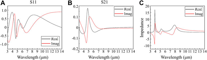
FIGURE 3. Calculated parameters of the Pt/Si multilayer based wavelength-selective absorber in 3–14 μm. (A) S11; (B) S21; (C) impedance.
According to the result of impedance calculation, in the high absorptivity band, the impedance of the absorber is closer to the impedance of air than in the low absorptivity band. Therefore, the incident electromagnetic wave can reach the ultrathin Pt layer in 5–8 μm band, causing a higher absorptivity, while most of the electromagnetic waves are reflected by the surface in atmospheric windows, resulting in a low absorptivity. Consequently, based on the impedance matching principle, the absorption characteristics of the absorber can be tuned by changing the thickness of Si layers. The four-layer structure can be prepared on substrates like stainless steel, polylactic acid (PLA), and other materials. Platinum can be deposited by magnetron sputtering or electron beam evaporation to control the thickness accurately, and silicon will be fabricated through electron beam evaporation for large-scale manufacturing.
The Wavelength-Selective Absorber in Terahertz Band (Compatible With Infrared)
Because the wavelength of electromagnetic waves in 0.1–2.7 THz is different from the infrared band, the designed wavelength-selective absorber above is not applicable. It is necessary to make some adjustments to the structure to maintain the selective absorption characteristics in the infrared band while improving the absorption performance of terahertz waves by constructing a certain microstructure on the surface.
Since the material has a structure similar to the Fabry-Perot cavity, the absorption performance requirements can be met by adjusting the thickness of the two Si dielectric spacers, while keeping the thickness of the ultrathin metal Pt layer and the bottom reflective Pt layer unchanged. For the reason of the wavelength of the terahertz band, the middle Si layer should be about 2000 nm thick to meet the absorption requirements. The RMSD between the calculated and ideal absorber is shown in Figure 4, as the thickness of the top and middle Si layer changed.
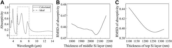
FIGURE 4. (A) Absorptivity of wavelength‐selective absorber. Root‐mean‐square deviation (RMSD) of the absorptivity relative to the ideal absorber with thickness changes. (B) in the middle Si spacer; (C) in the top Si spacer.
According to Figure 4, the thickness of the middle Si layer is 2055 nm and the thickness of the top Si layer is 1,263 nm which can relatively well achieve the wavelength-selective absorption that meets the requirements of infrared stealth. The thickness of the bottom Pt layer and the middle ultrathin Pt layer is 100 nm and 15 nm, respectively. At the same time, this structure can provide a foundation for the compatible absorption of terahertz waves.
Considering the convenience of processing and good absorption for both TE and TM waves, the surface microstructure should be designed as simple as possible with high symmetry. It was finally decided to select the surface microstructure as a periodic array of cylinders. Based on the Pt/Si four-multilayer structure, add a periodic array of Pt cylinders to the surface of the top Si layer to improve the absorption of the terahertz wave. Fix the height of cylinders to 0.2 μm, and calculate the absorptivity of the material at 0.1–2.7 THz while changing the radius of the cylinders; the curve of absorptivity is shown in Figure 5A.
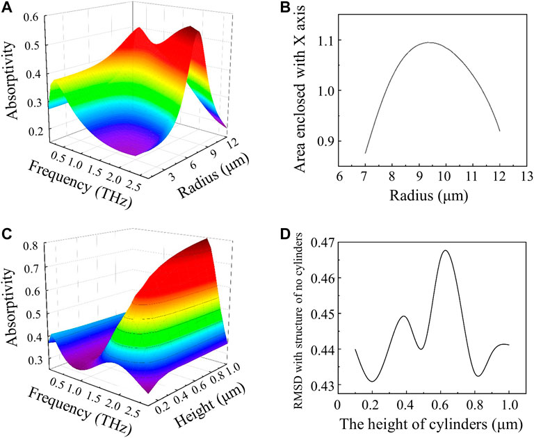
FIGURE 5. The absorptivity of material with parameters of cylinders changing in 0.1–2.7 THz. (A) radius; (C) height; (B) the area of absorptivity curves enclosed with X axis when radius of cylinders changing; (D) the root‐mean‐square deviation of absorptivity between structure with and without cylinders in infrared band when there are changes in the height of cylinders.
It can be seen that the position of the absorption peak in the terahertz band changes with the change of the radius of cylinders. In order to make the material absorb more electromagnetic waves in the target band, the area of absorptivity curves enclosed with the X-axis should be as large as possible. According to Figure 5B, when the radius of cylinders is 9.3 μm, the material has the best absorptive capacity. In 1–2.4 THz, the absorptivity of the material is all over 0.4.
Then adjust the height of cylinders and calculate the absorptivity curves of the material in 0.1–2.7 THz, shown in Figure 5C. At the same time, it is necessary to consider that the addition of microstructures should not have much influence on the absorptivity in the infrared band. Finally, the height of cylinders is determined to be 0.8 μm. It can be seen that the absorptivity curve has an absorption peak in 1.9–2.2 THz and the numerical value of the absorption peak is over 0.7. The absorptivity of the material in terahertz is shown in Figure 1C.
For the processing of the microstructure on the surface, it can use laser to process the array of cylinders, because platinum is not very hard to process. In order to improve the absorptivity of terahertz further, cylinders with different radius in a period could be used. As the radius of cylinder determines the position of the absorption peak, the superposition of several absorption peaks can broaden the absorption bandwidth that improves the absorption performance. This work proved that, by utilizing multilayer films and metamaterials, we can achieve compatible stealth in infrared and terahertz bands.
Conclusion
In conclusion, this research proposed a material with a simple structure and could be mass manufacturing based on multilayer film. The material has the ability of wavelength-selective absorption that meets the requirements of infrared stealth. By structural design, the calculated wavelength-selective absorber has low absorptivity in the two atmospheric windows (3–5 and 8–14 μm) and high absorptivity in the nonatmospheric window (5–8 μm), which has excellent stealth performance in the infrared band. Moreover, with the addition of a periodic array of Pt cylinders on the surface, the absorption capacity of the material in terahertz is significantly enhanced. Meanwhile, the material can still meet the performance requirements of stealth in an infrared band. This work may provide a new strategy for the compatible stealth in infrared and terahertz bands.
Data Availability Statement
The raw data supporting the conclusions of this article will be made available by the authors, without undue reservation.
Author Contributions
MZ and MY conceived and designed the research work. MY carried out the simulations. MY, JY, and YZ analyzed the data. MY wrote the paper. BX, WC, and XL contributed to helpful discussions to research and modification to the article.
Conflict of Interest
The authors declare that the research was conducted in the absence of any commercial or financial relationships that could be construed as a potential conflict of interest.
References
1. Liu X, Tyler T, Starr T, Starr AF, Jokerst NM, Padilla WJ. Taming the blackbody with infrared metamaterials as selective thermal emitters. Phys Rev Lett (2011) 107(4):045901. doi:10.1103/PhysRevLett.107.045901
2. Yang ZY, Ishii S, Yokoyama T, Dao TD, Sun M-G, Pankin PS, et al. Narrowband wavelength selective thermal emitters by confined tamm plasmon polaritons. ACS Photonics (2017) 4(9):2212–219. doi:10.1021/acsphotonics.7b00408
3. Shahsafi A, Joe G, Brandt S, Shneidman AV, Stanisic N, Xiao Y, et al. Wide-angle spectrally selective absorbers and thermal emitters based on inverse opals. ACS Photonics (2019) 6(11):2607–611. doi:10.1021/acsphotonics.9b00922
4. Du KK, Li Q, Lyu YB, Ding JC, Lu Y, Cheng ZY, et al. Control over emissivity of zero-static-power thermal emitters based on phase-changing material GST. Light Sci Appl (2017) 6(1):e16194. doi:10.1038/lsa.2016.194
5. Kecebas MA, Menguc MP, Kosar A, Sendur K. Passive radiative cooling design with broadband optical thin-film filters. J Quant Spectrosc Radiat Transf (2017) 198:179–86. doi:10.1016/j.jqsrt.2017.03.046
6. Doiron CF, Naik GV. Non-hermitian selective thermal emitters using metal-semiconductor hybrid resonators. Adv Mater (2019) 31(44):e1904154. doi:10.1002/adma.201904154
7. Mu X, Yu X, Xu D, Shen X, Xia Z, He H, Zhu H, et al. High efficiency organic/silicon hybrid solar cells with doping-free selective emitter structure induced by a WO3 thin interlayer. Nano Energy (2015) 16:54–61. doi:10.1016/j.nanoen.2015.06.015
8. Ding D, Lu G, Li Z, Zhang Y, Shen W. High-efficiency n-type silicon PERT bifacial solar cells with selective emitters and poly-Si based passivating contacts. Solar Energy (2019) 193:494–501. doi:10.1016/j.solener.2019.09.085
9. Kim J, Yun JH, Kim H, Cho Y, Park HH, Kumar MM, et al. Transparent conductor-embedding nanocones for selective emitters: optical and electrical improvements of Si solar cells. Sci Rep (2015) 5(1):9256–8. doi:10.1038/srep09256
10. Bhatt R, Kravchenko I, Gupta M. High-efficiency solar thermophotovoltaic system using a nanostructure-based selective emitter. Solar Energy (2020) 197:538–45. doi:10.1016/j.solener.2020.01.029
11. Chen Y B, Parashar P, Yang YH, Rawat T S, Chen SW, Shen CH, et al. Transparent planar indium tin oxide for a thermo-photovoltaic selective emitter. Opt Mater Express (2020) 10(9):2330–44. doi:10.1364/OME.397246
12. Hassan S, Doiron CF, Naik GV. Optimum selective emitters for efficient thermophotovoltaic conversion. Appl Phys Lett (2020) 116(2):023903. doi:10.1063/1.5131367
13. Park C, Kim J, Hahn JW. Selective emitter with engineered anisotropic radiation to minimize dual-band thermal signature for infrared stealth technology. ACS Appl Mater Interfaces (2020) 12(38):43090–97. doi:10.1021/acsami.0c12283
14. Zhao L, Liu H, He Z, Dong S. All-metal frequency-selective absorber/emitter for laser stealth and infrared stealth. Appl Opt (2018) 57(8):1757–64. doi:10.1364/AO.57.001757
15. Kim J, Han K, Hahn JW. Selective dual-band metamaterial perfect absorber for infrared stealth technology. Sci Rep (2017) 7(1):6740–9. doi:10.1038/s41598-017-06749-0
16. Chen X, Tian C, Che Z, Chen T. Selective metamaterial perfect absorber for infrared and 1.54 μm laser compatible stealth technology. Optik (2018) 172:840–46. doi:10.1016/j.ijleo.2018.07.091
17. Zhong S, Wu L, Liu T, Huang J, Jiang W, Ma Y. Transparent transmission-selective radar-infrared bi-stealth structure. Opt Express (2018) 26(13):16466–76. doi:10.1364/OE.26.016466
18. Peng L, Liu D, Cheng H, Zhou S, Zu M. A multilayer film based selective thermal emitter for infrared stealth technology. Adv Opt Mat (2018) 6:1801006. doi:10.1002/adom.201801006
19. Moghimi M J, Lin G, Jiang H. Broadband and ultrathin infrared stealth sheets. Adv Eng Mater. (2018) 20(11):1800038. doi:10.1002/adem.201800038
20. Cen C, Zhang Y, Liang C, Chen X, Yi Z, Duan T, et al. Numerical investigation of a tunable metamaterial perfect absorber consisting of two-intersecting graphene nanoring arrays. Phys Lett A (2019) 383(24):3030–35. doi:10.1016/j.physleta.2019.06.028
21. Kawamoto Y, Tanaka Y, Ishizaki K, De Zoysa M, Asano T, Noda S. Structural optimization of photonic crystals for enhancing optical absorption of thin film silicon solar cell structures. IEEE Photonics J (2014) 6(1):1–10. doi:10.1109/jphot.2014.2302800
22. Hajian H, Ghobadi A, Butun B, Ozbay E. Nearly perfect resonant absorption and coherent thermal emission by hBN-based photonic crystals. Opt Express (2017) 25(25):31970–87. doi:10.1364/OE.25.031970
23. Gomez-Diaz JS, Tymchenko M, Lee J, Belkin MA, Alù A. Nonlinear processes in multi-quantum-well plasmonic metasurfaces: electromagnetic response, saturation effects, limits, and potentials. Phys Rev B (2015) 92(12):125429. doi:10.1103/PhysRevB.92.125429
24. Shvonski AJ, Kong J, Kempa K. Nonlocal extensions of the electromagnetic response of plasmonic and metamaterial structures. Phys Rev B (2017) 95(4):045149. doi:10.1103/PhysRevB.95.045149
25. Dai J, Xu R, Lin YS, Chen CH. Tunable electromagnetic characteristics of suspended nanodisk metasurface. Opt Laser Technol (2020) 128:106214. doi:10.1016/j.optlastec.2020.106214
26. Zhao X, Zhang J, Fan K, Duan G, Metcalfe GD, Wraback M, et al. Nonlinear terahertz metamaterial perfect absorbers using GaAs [Invited]. Photon Res (2016) 4(3):A16–21. doi:10.1364/PRJ.4.000A16
27. Yang J, Gong C, Sun L, Chen P, Lin L, Liu W. Tunable reflecting terahertz filter based on chirped metamaterial structure. Sci Rep (2016) 6:38732. doi:10.1038/srep38732
28. Manjappa M, Pitchappa P, Wang N, Lee C, Singh R. Active control of resonant cloaking in a terahertz MEMS metamaterial. Adv Opt Mat (2018) 6(16):1800141. doi:10.1002/adom.201800141
29. Dao R, Kong X, Zhang H, Su X. A tunable broadband terahertz metamaterial absorber based on the vanadium dioxide. Optik (2019) 180:619–25. doi:10.1016/j.ijleo.2018.12.004
30. Zhu J, Ma Z, Sun W, Ding F, He Q, Zhou L, et al. Ultra-broadband terahertz metamaterial absorber. Appl Phys Lett (2014) 105(2):021102. doi:10.1063/1.4890521
31. Jung H, Jo H, Lee W, Kim B, Choi H, Kang MS, et al. Electrical control of electromagnetically induced transparency by terahertz metamaterial funneling. Adv Opt Mat (2019) 7(2):1801205. doi:10.1002/adom.201801205
Keywords: wavelength-selective, compatible absorber, infrared, terahertz, multilayer, microstructure
Citation: Yang M, Zhou M, Yu J, Zhang Y, Xu B, Cheng W and Li X (2021) Infrared and Terahertz Compatible Absorber Based on Multilayer Film. Front. Phys. 9:633971. doi: 10.3389/fphy.2021.633971
Received: 26 November 2020; Accepted: 04 January 2021;
Published: 17 February 2021.
Edited by:
Fuli Zhang, Northwestern Polytechnical University, ChinaReviewed by:
Yongqiang Pang, Xi’an Jiaotong University, ChinaJiafu Wang, Air Force Engineering University, China
Copyright © 2021 Yang, Zhou, Yu, Zhang, Xu, Cheng and Li. This is an open-access article distributed under the terms of the Creative Commons Attribution License (CC BY). The use, distribution or reproduction in other forums is permitted, provided the original author(s) and the copyright owner(s) are credited and that the original publication in this journal is cited, in accordance with accepted academic practice. No use, distribution or reproduction is permitted which does not comply with these terms.
*Correspondence: Ming Zhou, emhvdW1pbmdAdHNpbmdodWEuZWR1LmNu