 Stephane A. Boubanga-Tombet1
 Akira Satou1
 Deepika Yadav1
 Dmitro B. But2,3Wojciech Knap1,2,4
 Vyacheslav V. Popov5
 Ilya V. Gorbenko6
 Valentin Kachorovskii2,6
 Taiichi Otsuji1*
- 1Research Institute of Electrical Communication, Tohoku University, Sendai, Japan
- 2CENTERA Laboratories, Institute of High Pressure Physics PAS, Warsaw, Poland
- 3CEZAMAT, Warsaw Technical University, Warsaw, Poland
- 4Laboratory Charles Coulomb, University of Montpellier and CNRS, Montpellier, France
- 5Kotelnikov Institute of Radio Engineering and Electronics (Saratov Branch), RAS, Saratov, Russia
- 6Ioffe Institute, St. Petersburg, Russia
This study reviews recent advances in room-temperature coherent amplification of terahertz (THz) radiation in graphene, electrically driven by a dry cell battery. Our study explores THz light–plasmon coupling, light absorption, and amplification using a current-driven graphene-based system because of its excellent room temperature electrical and optical properties. An efficient method to exploit graphene Dirac plasmons (GDPs) for light generation and amplification is introduced. This approach is based on current-driven excitation of the GDPs in a dual-grating-gate high-mobility graphene channel field-effect transistor (DGG-GFET) structure. The temporal response of the DGG-GFETs to the polarization-managed incident THz pulsation is experimentally observed by using THz time-domain spectroscopy. Their Fourier spectra of the transmitted temporal waveform through the GDPs reveals the device functions 1) resonant absorption at low drain bias voltages below the first threshold level, 2) perfect transparency between the first and the second threshold drain bias levels, and 3) resonant amplification beyond the second threshold drain bias voltage. The maximal gain of 9% is obtained by a monolayer graphene at room temperatures, which is four times higher than the quantum limit that is given when THz photons directly interact with electrons. The results pave the way toward tunable graphene plasmonic THz amplifiers.
Introduction
Graphene is promised to a wealth of interesting applications, and graphene plasmonics is emerging as one of the most viable paths for bringing those applications into reality [1, 2]. Over the past years, noble metal/semiconductor plasmonics has allowed significant progress in a number of fields with impressive applications to ultrasensitive detection down to the single-molecule level [3], improved photovoltaics [4], nanoscale photometry [5], and cancer therapy [6]. Nevertheless, graphene is currently taking off as one of the most vibrant and promising alternatives in the race for new plasmonic materials [7], especially in the mid to far-infrared (THz) regions [8–14].
The generation and amplification of electromagnetic waves by plasmonic instabilities in conventional two-dimensional (2D) electron systems (2DESs) have been actively investigated since 1980. The main idea has been to exploit the radiative decay of grating-coupled 2D plasmons for the realization of compact tunable solid-state far-infrared devices [15–27] and thus develop new alternatives to the vacuum devices, such as traveling wave and backward wave tubes based on the Smith–Purcell effect [28], which face severe difficulties to operate beyond the millimeter-wave region [29]. However, after about 40 years, we are still a long way from the realization of efficient emitters, amplifiers, and generators based on those plasmonic instability–driven mechanisms. The intensity of radiation reported experimentally so far is too small [16, 24–26], and the plasmon resonances are too broad and not tunable enough [27] to be promising for device applications.
The rise of graphene and the well-established stronger light–plasmon coupling in graphene structures compared to conventional 2DES’s in semiconductor materials [30] make this work worth to be revisited. Indeed, graphene plasmon–based far-infrared devices have recently been investigated [31–34] and significant improvements on gain modulation [32, 34], sensitivity [33], and emission [31] have been reported, yielding the foundational pillars for a future robust graphene-based plasmonic technology from mid- to far-infrared region. Therefore, to address the efficiency limitation of conventional 2D plasmonic grating-coupled emitters and amplifiers, we explore a graphene plasmonic approach.
We investigate dc current-driven plasmonic amplification in high-mobility graphene-channel transistor GFET structures that combine the advantage of an efficient tunable absorber, emitter, and amplifier at room temperatures. Plasmon modes in our devices are excited in monolayer graphene encapsulated in hexagonal boron nitride (hBN) layers with a periodic grating gate structure positioned above the graphene sheets as used elsewhere in 2D semiconductors [22, 35–42]. The grating gate modulates the incoming electromagnetic wave and defines the plasmonic wave vectors.
This is the first experimental observation of such plasmon dynamics with clear transitions from absorption to transparency and then amplification regimes, explained here by the occurrence of current-driven plasmonic instabilities and/or negative conductivities and the resulting plasmon-polariton gain in the graphene DGG structures. The external quantum efficiency extracted from our devices is about ∼0.1 (see Supplementary Material S0) which is several orders of magnitude higher than the largely used optical-to-THz conversion devices since the work by Auston at al. [43] on picosecond photo-conducting Hertzian dipoles in 1984, and about two orders of magnitude higher than the plasmon-improved photo-conducting devices based on conventional semiconductors [44, 45].
The main part of the experimental results has been published in the authors’ original prior publications [46, 47] which will be re-reviewed and be extended in their interpretations in this article. The interpretation of the observed phenomena of THz amplification with existing theories was given in [46], which will be emphasized with a different route to trace the scenario with new theories [47].
Device Fabrication and Experimental Setup
We designed a series of monolayer graphene channel field-effect transistor (GFET) structures. First, a hexagonal boron nitride (hBN) thin film was exfoliated from a bulk material and transferred onto a SiO2/Si substrate as a buffer base layer. Then, a high-quality monolayer graphene was exfoliated from a kish graphite single crystal, and transferred onto the hBN buffer layer. Then another thin hBN film was transferred onto the monolayer graphene to encapsulate the graphene and to work for the gate stack insulator. Then the gate electrodes were metalized and lifted off to form our original dual-grating-gate (DGG) structure that worked as a highly efficient antenna to couple the THz radiations and graphene Dirac plasmons (GDPs) [46, 47]. By the Raman spectroscopy and the contrast differentiations of the optical microscope image, the transferred graphene sheet was well identified to be monolayer. The DC characteristics were measured, confirming a fine electrical ambipolar transfer characteristic with less unintentional doping (as shown in Supplementary Materials S1, Supplementary Figure S1D). The extracted electron field-effect mobility ranged between 30,000 and 40,000 cm2/Vs, depending on the DGG and drain biases conditions, thanks to the hBN-encapsulated cleanest and inert environment [46, 47].
We examined three samples: two asymmetric DGG alignments (A-DGG1 shown in Figure 1B and A-DGG2 shown in Supplementary Materials S1, Supplementary Figure S1C) [46] and one symmetric DGG alignment (S-DGG, shown in Figure 1C). Details on samples description are given in the Supplementary Materials S1. With the applied gate voltages Vg1 and Vg2, each device supports the formation of two different plasmonic cavities (types C1 and C2) below the DGG fingers of Gate 1 and Gate 2 (see top part of Figure 1A).
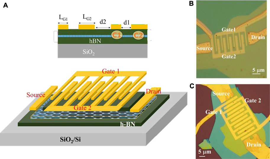
FIGURE 1. Schematic view and device images of the DGG-GFETs. Schematic illustrating of the hBN/graphene/hBN heterostructure, including the asymmetric dual-grating-gate metallization (A). Optical image of the asymmetric dual-grating-gate A-DGG1 (B) and the symmetric S-DGG (C) samples. After Ref. 46.
Terahertz time-domain spectroscopy (THz-TDS) was employed to measure the changes in the temporal wave forms of the THz pulses transmitted through the graphene plasmonic cavities of type C1 (C2) when sweeping Vg1 (Vg2) and keeping the voltage on the other gate electrode constant at the charge neutral point (CNP) Vg2 = VCNP2 (Vg1 = VCNP1). The THz pump pulse was generated by a low temperature–grown InGaAs/InAlAs photoconductive antenna (TERA 15-TX, Menlosystems) excited by a femtosecond 1550-nm band fiber-laser pulse source (IMRA femtolite BS-60: <100 fs FWHM, 50 Hz repetition, >60 mW average output power). The linearly polarized THz wave emitted by the antenna was collected and refocused onto the sample from 45° oblique angle (and subsequently onto the THz detector) using off-axis parabolic mirrors. A small 250-μm-diameter hole at the end of a tapered aperture of a conical shape was placed close to the sample. THz radiation was detected using a second low temperature–grown InGaAs/InAlAs THz photoconductive antenna made of the 25-μm dipole and 10-μm gap excited with an average optical power of 17 mW (at 1,550 nm). More detailed information about the experimental setup is given in Ref. 47. The measurement system bandwidth was 0.1–4 THz and the S/N of ∼40 dB. The source-to-drain voltage (Vd)–dependent measurements were also conducted at a constant Vg1,2. The transmission coefficient was obtained by the fraction of the Fourier transform from the measured temporal waveform of the signal transmitted through and without the device. The transmission coefficient at a given Vg1 (g2) and Vd is referred to as T, whereas TCNP is the transmission coefficient at Vg1 (g2) = VCNP.
Experimental Results
Results Under Non-Drain–Biased Conditions
Figure 2 depicts the measured extinction spectra (1−T/TCNP) in the three devices for Vd = 0 V. The gate length–dependent extinction spectra are shown in Figures 2A,B for the same electrical doping of one type of cavities (C1 or C2) Vg1,2 − VCNP = 3 V, while the other type of cavities (C2 or C1) is in the CNP conditions. The incident THz radiation was polarized parallel (Figure 2A) or perpendicular (Figure 2B) to the DGG fingers. In the parallel polarization case, the extinction spectra are characterized by the Drude response with a monotonic decrease of the absorption with frequency. In the perpendicular polarization, in contrast, a completely different line shape is seen with a pronounced absorption peak associated with the excitation of the plasmons resonance. We used a damped oscillator
where
is the plasma wave velocity. q is the plasma wave vector, d is the thickness of the top h-BN layer, e is the elementary charge, ε is the dielectric constant of h-BN layers, εF is the Fermi energy, and ℏ is the reduced Planck constant. We observed up to ∼19% absorption in the sample S-DGG (LG = 2 µm) which is substantially strong for a single atomic layer material, testifying of a strong light to plasmon coupling in our devices.
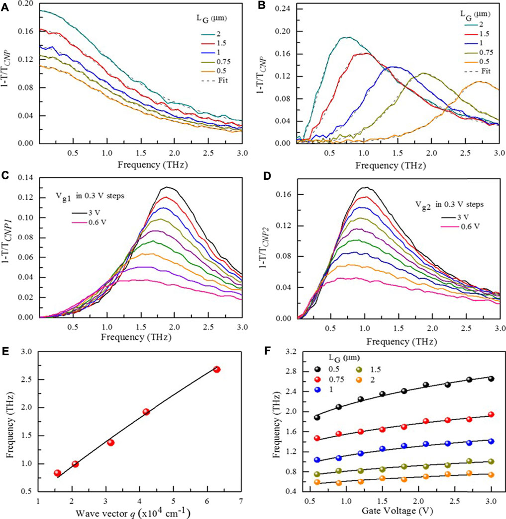
FIGURE 2. Gate voltage– and length-dependent extinction spectra of the graphene structures for Vd = 0 V. Plasmonic cavity length (LG)–dependent extinction spectra of the three devices with incident light polarized parallel (A) and perpendicular (B) to the DGG fingers. The measured line shape is well reproduced by a Drude model fit for parallel polarization [dashed line in (A)] and a damped oscillator model fit for perpendicular polarization [dashed line in (B)]. Measured gate voltage–dependent transmission spectra 1−T/TCNP of the asymmetric device A-DGG1 with incident light polarized perpendicular to the DGG fingers, with biased cavities C1 when sweeping Vg1, while the voltage on the other gate electrode is kept constant at Vg2 = VCNP2(C) and biased cavities C2 when sweeping Vg2, while the voltage on the other gate electrode is kept constant at Vg1 = VCNP1(D). Scaling laws of graphene plasmon resonance frequency in the three devices as a function of wave vector q = π/LG(E) and gate voltage (F). The solid lines in (E) and (F) are fits to data using the model expressed in Eq. 1. After Ref. 46.
To study the resonance scaling behavior with the carrier density, we conducted bias-dependent measurements. The gate voltage–dependent extinction spectra are shown in Figures 2C,D for the device A-DGG1 with light polarized perpendicular to the gate fingers for different values of Vg1, while Vg2 = VCNP2 (Figure 2C) and different values of Vg2 while Vg1 = VCNP1 (Figure 2D). It is worth mentioning that throughout all of our experiments, the data from the other devices (A-DGG2 and S-DGG) were quite similar to that shown in Figures 2C,D (see also the Supplementary Materials S2). Our gate voltage–dependent data also show a clear blue shift of absorption peak frequency with increasing Vg and an increase in the strength of the plasmon resonance. The scaling behavior of plasmon resonance frequency is shown in Figures 2E,F where the resonance peak extracted from the measured extinction are plotted as a function of the plasmon wave vector q = π/LG (Figure 2E) and gate voltage (Figure 2F) and fitted to Eq. 1 for the dispersion law of gated 2D plasmons in graphene with hBN layer thickness as a parameter.
Our data show good agreement between the measured resonance frequencies scaling laws over carrier density and cavity length and the theoretical expectations, allowing us to unambiguously attribute the resonances observed here to GDPs in the DGG-GFET’s. The plasmon absorption coefficients obtained in our graphene structures, with metallic gates-induced plasmonic cavities are rather high, compared to the previously reported results in graphene micro-ribbons [30, 50, 51], rings, and disks [11, 52, 53].
Results Under Drain-Biased Conditions
The most striking features in our measurements arise when we explore the influence of Vd on the device absorption spectra. Figure 3 depicts the Vd-dependent extinction spectra measured in the cavities C1 and C2 of the sample A-DGG1 with the electrical doping at Vg1 − VCNP1 = 3 V, Vg2 = VCNP2 (Figures 3A,C) and Vg2 − VCNP2 = 3 V, Vg1 = VCNP1 (Figures 3B,D). As Vd increases, the absorption peak clearly exhibits the red shifting along with a noticeable reduction of plasmon resonance strength. Then the absorption completely vanishes, as seen in the measured extinction spectra being zero at Vd = 160 mV (Figure 3A) and Vd = 370 mV (Figure 3B). The plasmonic devices become perfectly transparent to the incoming THz radiation within the entire experimental bandwidth. Here we report the first experimental observation of such a transparency behavior over a relatively wide frequency range (0.1–3 THz) in graphene plasmonic structures at 300 K. With increasing Vd beyond this transparency regime, a negative absorption peak appears in the extinction spectra from the lower frequency side with a noticeable blue shift. The negative absorption is an indication of a more intense transmitted pulse as compared to the incoming pulse referred to as gain. This striking influence of Vd can also be visualized in inversion of the experimental extinction spectra as a function of frequency and Vd as shown in Figure 3 where the positive peaks in red-colored spectra show the device absorption, whereas the negative peaks in blue-colored spectra show the gain, and the transparency regime between the two peaks with clear current-induced transitions between those regions. Throughout all of our experiments, the data from the other asymmetric device (A-DGG2) were quite similar to those shown in Figure 3, while no amplification was observed in the symmetric sample S-DGG (see the Supplementary Materials S3) [46].
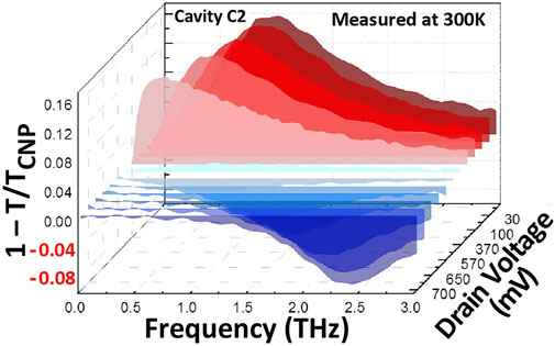
FIGURE 3. Drain bias–dependent extinction spectra of the graphene structures. Spectra measured in cavity C2 of device A-DGG1 for fixed Vg2 − VCNP2 = 3 V and Vg1 = VCNP1 when varying Vd. After Ref. 46.
Discussion
Interpretation of the Phenomena on the Basis of Classical Theories
By assuming that the carrier drift velocity (v0) is proportional to the mobility and dc electric field in each cavity we estimate that v0 varies from 0 to ∼3.85
We now examine the scaling behavior of plasmon resonance frequency with drain bias voltages. The resonance frequencies, ωP(Vd) extracted from the drain voltage–dependent extinction spectra for the asymmetric devices are shown in Figure 4A as a function of the characteristic field intensity qVd in the plasmonic cavities. In the positive absorption region, the plasmon resonance frequencies are described by a scaling behavior of ωP(Vd) = ωP (0)[1 − αqVd]β, while in the negative absorption region (amplification region), the scaling behavior is ωP(Vd) = ζ [−1 + χqVd]η. Our fitting (solid lines in Figure 4A) gives β ≈ 0.3 and η ≈ 0.5, while the parameter α ≈ 0.37 (kV/cm)−1 defining the lower cut-off, the same in all cavities, indicates that the onset of the observed transparency regime depends only on the dc electric field in the plasmonic cavities. However, the amplification onset defined by the fitting parameter χ ≈ 0.098, 0.127, 0.149, and 0.187 (kV/cm)−1 for LG = 1.5, 1, 0.75, and 0.5 µm varies for different cavities. This cavity length–dependent amplification threshold has been predicted in symmetrical plasmonic cavities based on conventional 2DES [18], although it was formulated for case wherein the carrier drift velocity surpasses the plasma velocity which is ruled out in this experiment. In the presence of Vd, the source–drain current introduces a collective electron stream flow on which plasma waves are carried at drift velocity v0. Physical phenomena such as Doppler shift of plasmon frequency might therefore occur in the plasmonic system and be considered as possible explanation for the red and blue shift observed experimentally. However, the experimental current-induced tuning range of the resonance frequencies is wider than that expected from a simple classical model. Theoretical approach including the nontrivial carrier hydrodynamics in graphene, the nonuniform density in the channel and asymmetric grating gates remain an open challenge for rigorous quantitative interpretation of the observed drain voltage–dependent scaling behavior of plasmon resonance frequencies.
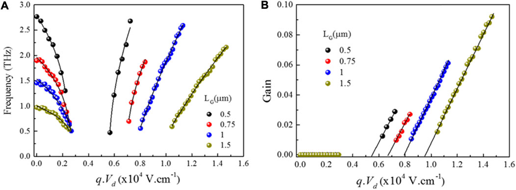
FIGURE 4. Drain bias–dependent resonance frequencies (A) and gain (B). Scaling laws of the measured graphene plasmon resonance frequency in the three devices as a function of qVd and fits to data shown as solid lines (A). Maximal gain coefficient (minima of the negative extinction spectra) measured in devices A-DGG1 and A-DGG2 (B). Clear threshold-like behavior is seen with onset field intensities of ∼ 5.4 kV/cm (black dotes), ∼6.6 kV/cm (red dotes), ∼7.8 kV/cm (blue dotes), and ∼9.4 kV/cm (dark yellow dotes) in the four cavities. After Ref. 46.
Figure 4B depicts the maximal gain coefficient obtained in the two asymmetric samples as a function of qVd. The applied drain bias voltage varies up to 700 mV with the incoming THz radiation power of the order of few microwatts. Our data show up to ∼9% amplification, which is remarkably high for a single atomic material, testifying of a relatively efficient plasmonic generation process and strong plasmon–radiation coupling. We define the external quantum efficiency as EQE = Pout/Pin where Pout is the device emitted power and Pin the injection power. We estimate Pout ≈ 2.7 µW in our graphene-based devices, while the injection electrical power is Pin ≈ 32 µW by considering the upper limit of Vd = 700 mV and the protection current limit of Ip = 1 µA set to keep the devices safe during experiments. Our devices therefore demonstrate significantly high external quantum efficiency EQE ≈ 0.1 (see Supplementary Materials S1). While relatively inefficient plasmon generation has been reported in semiconductor heterostructures [16, 22, 24–26], the improved efficiency observed in our DGG-GFET devices is consistent with the well-established stronger light–plasmon coupling in graphene structures compared to conventional 2DES in semiconductor materials [30]. Other types of sources operating at 300 K such as the optical-to-THz conversion photoconductive devices are largely used in THz technologies. Recently, plasmon based photoconductive devices have shown improved performance in terms of bandwidth and power [44, 45] with a maximum emitted power of 250 µW for 80 V bias voltage and 100 mW optical pump power [44] and thus an external quantum efficiency of the order of ∼10−3. Our graphene plasmonic devices show about two orders of magnitude higher external quantum efficiency as compared to those improved optical-to-THz conversion photoconductive devices.
The gain is observed beyond threshold field intensities of ∼5.4 kV/cm (black dotes), ∼6.6 kV/cm (red dotes), ∼7.8 kV/cm (blue dotes), and ∼9.4 kV/cm (dark yellow dotes) in the four cavities as shown in Figure 4A. This threshold-like behavior indicates that the current-driven plasmonic instability is likely to be the process governing the occurrence of plasmon generation in our hBN/graphene/hBN structures. In this subsection, we discuss the possible origins of plasmon instability in our structures by first ruling out the physical mechanisms requiring carrier drift velocities higher than plasmon velocities since the estimated plasmon velocity in our structures s ≈ 3 × 108 cm/s is higher than the maximum drift velocity v0 = 3.85 × 107 cm/s.
Theoretical investigations of such instabilities have been developed in 2DES based on conventional semiconductor heterostructures [15, 17, 18, 20, 21, 54, 55] and different scenarios are predicted depending on the fraction of carrier drift velocity v0 and plasma velocity s. For values of v0 smaller than s, an instability based on amplified plasmon reflection at the cavity boundaries are predicted in Ref. 17, if asymmetrical boundary conditions are realized at different ends of the cavity. In Refs. 19, 57, 58, it has been shown that transit time effects in the high field domains of 2DES may drive the plasmonic system unstable, no matter which velocity is higher than the other, v0 or s. When the drift velocity reaches the plasma velocity, a different type of instability named dissipative instability [15] may develop along with a choking of electron flow leading to the current saturation [56]. Another type of plasmonic instability, which is not our case, has been predicted for the carrier drift velocity surpassing the plasmon velocity referred as plasmonic boom instability occurring with a super-plasmonic boom similar to the well-known supersonic boom [20]. Cherenkov-like plasmon instability may also develop in the grating gated 2D electron structure when the electron drift velocity exceeds the plasmon phase velocity [18, 21].
On the basis of the experimental results where the carrier drift velocity is always lower than the plasma velocity, amplified plasmon reflection at the cavity boundaries [17] and transit time effects [19, 57, 58] are therefore most likely to be the main process governing the observed transparency and gain. Indeed, giant plasmon instability has been predicted in graphene plasmonic structures similar to those reported in the present work, when the amplified reflection and transit-time–based type of instabilities are superposed with phase synchronization between the neighboring cavities [58].
The common ground within the plasmonic instability picture is the wave amplitude growth with an increase in the electron drift velocity [15, 17, 18, 20, 21]. The plasmon gain also known as instability increment then acts against the plasma wave damping responsible for the losses. The emission is observed above the drift velocity threshold where the gain becomes bigger than the losses. The instability increment,
where J0(x) is the zeroth order Bessel function, Lt/ut is the electron transit time from one plasmonic cavity to the other one, ut and Lt are the drift velocity in the transit regions and the length of those regions, respectively. The decrement is given by γd = ΓP/2, where ΓP is the plasmon resonance line width, which is ∼0.6 THz around the lower cut-off defined by the occurrence of the transparency regime. By assuming ut ∼ Fermi velocity (vF) in the depleted regions, we obtain γi ≈ 0.87 THz. This increment is bigger than the decrement which supports the idea of the two types of instabilities being the governing mechanisms of the observed amplification.
The drain voltage–dependent phase change retrieved from the THz electric field in cavities for ADGG-GFETs manifested the inversion between the absorption and amplification conditions (see Supplementary Materials S4). This transition is an unambiguous evidence for gain and additionally supports our interpretation of light amplification via excitation of graphene Dirac plasmons in the high-mobility hBN/graphene/hBN structures.
Interpretation on the Basis of a New Phenomenological Modeling
The most important theoretical challenge is to find the physical process or mechanism in which the transition from absorption with red shift to amplification with blue shift can take place for drift velocities v below the plasma wave velocity s. In this work, we develop a phenomenological theory which shows that, indeed, amplification is possible for v < s [47]. We use grating gate structures to create a periodic structure of highly conducting active regions separated by low conducting passive regions. The large difference between concentrations allows us to localize plasmons in active regions and control their properties both by gate electrodes and by the dc driving current. Let us consider the structure of periodically alternated stripes of the high (low) electron density and corresponding high (low) plasma wave velocity, as shown in Figure 5 composed of two different regions with lengths L1 and L2, plasma velocities s1 and s2, carrier densities n1 and n2, and drift velocities v1 and v2 (see Figure 5). This periodic structure (plasmonic crystal) can be described by the Kronig–Penney model [59]. We assume that n1 ≫ n2 and refer to region “1” as active and region “2” as passive. In the absence of dissipation, such a structure represents an example of 1D plasmonic crystal [47], with the plasma wave spectrum
where k is the plasmon quasi-momentum,
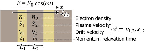
FIGURE 5. A simplified 1D hydrodynamic modeling for the DGG structure driven by dc current in the oscillating field of the THz radiation E.
One may linearize the hydrodynamic equations of graphene Dirac plasmons as follows [47]:
where
In this case, the plasmons in passive region 2 are overdamped, whereas the plasmons in active region 1 may oscillate at resonant frequencies. Here, we introduce an effective plasmon relaxation rate (inverse of the effective plasmon relaxation time) as follows:
One may find the solutions in the form of
The dependence of total averaged dissipation
Eq. 11 contains plasmonic resonance characterized by the effective frequency
The calculated
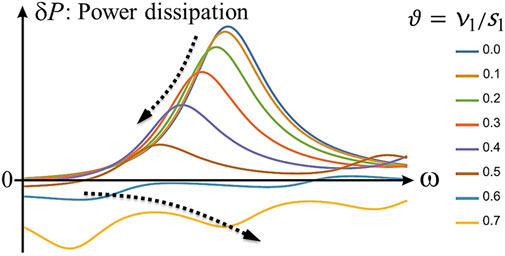
FIGURE 6. Calculated power dissipation in the active region 1 for different values of
Conclusion
In summary, we have introduced an efficient method to exploit graphene Dirac plasmons for light generation and amplification. This approach is based on asymmetric dual-grating-gate high-mobility graphene-channel FETs, but can potentially be applied in other emerging 2D materials with low level of losses and high degree of spatial confinement of plasmons. This work answers the problems stated about 40 years ago about the possibility of using the radiative decay of grating-coupled 2D plasmons for the creation of tunable compact solid-state based THz emitters and amplifiers. Interpretations for the observed phenomena, drain voltage–dependent transition from absorption with red shift to amplification with blue shift via transparent regime, are given in two ways based on plasmonic instabilities and non-plasmonic instabilities. The plasmonic instabilities in 2DESs is a reliable method for THz light generation in contrast to optical down-conversion to THz frequencies based on nonlinear optical effects and the optical-to-THz conversion through photoconduction, the latter present a very low conversion efficiency and the former is also inherently inefficient due to the optical and THz phase mismatch limiting the efficient field interaction length. Our new phenomenological device modeling suggested a possibility of plasmonic amplification mechanism without the need for instabilities. Moreover, while other types of emitters such as quantum-cascade lasers operate exclusively at cryogenic temperatures, all results presented in this work are obtained at room temperatures. The graphene plasmonic solutions presented here offer new ways for designing efficient devices for future robust far-infrared plasmonic technology and establish new important challenges for theoretical physics still requiring a physical model allowing full quantitative description of current-driven plasma phenomena in graphene and other 2D systems with Dirac like energy band structure.
Author Contributions
SB-T was primarily responsible for experimental works. DY and AS supported the experimental works. AS, WK, and VK are primarily responsible for theoretical works. VP and DB supported the theoretical works. TO supervised the entire work and was responsible for experimental works. All the authors contributed equally to write and edit the manuscript.
Funding
The work was supported by JSPS KAKENHI (No. 20K20349 and No. 21H04546), Japan; the International Research Agendas program of the Foundation for Polish Science co-financed by the European Union under the European Regional Development Fund for CENTERA (No. MAB/2018/9); and the Foundation for Polish Science through the TEAM Project No. POIR.04.04.00-00-3D76/16 (TEAM/2016-3/25). The work of IG and VK was supported by Russian Foundation of Basic Research (Grant No. 20-52-12019). The work of VP was carried out within the framework of the state task.
Conflict of Interest
The authors declare that the research was conducted in the absence of any commercial or financial relationships that could be construed as a potential conflict of interest.
Publisher’s Note
All claims expressed in this article are solely those of the authors and do not necessarily represent those of their affiliated organizations, or those of the publisher, the editors and the reviewers. Any product that may be evaluated in this article, or claim that may be made by its manufacturer, is not guaranteed or endorsed by the publisher.
Acknowledgments
We thank V. Ryzhii, S. Mikhailov, D. Svintsov, K. Maussang, M. S. Shur, and M. Dyakonov for many useful discussions.
Supplementary Material
The Supplementary Material for this article can be found online at: https://www.frontiersin.org/articles/10.3389/fphy.2021.726806/full#supplementary-material
References
1. Castro Neto AH, Guinea F, Peres NMR, Novoselov KS, Geim AK. The Electronic Properties of Graphene. Rev Mod Phys (2009) 81:109–62. doi:10.1103/revmodphys.81.109
2. Bonaccorso F, Sun Z, Hasan T, Ferrari AC. Graphene Photonics and Optoelectronics. Nat Photon (2010) 4:611–22. doi:10.1038/nphoton.2010.186
3. Kneipp K, Wang Y, Kneipp H, Perelman LT, Itzkan I, Dasari RR, et al. Single Molecule Detection Using Surface-Enhanced Raman Scattering (SERS). Phys Rev Lett (1997) 78:1667–70. doi:10.1103/physrevlett.78.1667
4. Atwater HA, Polman A. Plasmonics for Improved Photovoltaic Devices. Nat Mater (2010) 9:205–13. doi:10.1038/nmat2629
5. Knight MW, Sobhani H, Nordlander P, Halas NJ. Photodetection with Active Optical Antennas. Science (2011) 332:702–4. doi:10.1126/science.1203056
6. Loo C, Lowery A, Halas N, West J, Drezek R. Immunotargeted Nanoshells for Integrated Cancer Imaging and Therapy. Nano Lett (2005) 5:709–11. doi:10.1021/nl050127s
7. West PR, Ishii S, Naik GV, Emani NK, Shalaev VM, Boltasseva A. Searching for Better Plasmonic Materials. Laser Photon Rev (2010) 4:795–808. doi:10.1002/lpor.200900055
8. Grigorenko AN, Polini M, Novoselov KS. Graphene Plasmonics. Nat Photon (2012) 6:749–58. doi:10.1038/nphoton.2012.262
9. Koppens FHL, Chang DE, García de Abajo FJ. Graphene Plasmonics: A Platform for Strong Light-Matter Interactions. Nano Lett (2011) 11:3370–7. doi:10.1021/nl201771h
10. Jablan M, Buljan H, Soljačić M. Plasmonics in Graphene at Infrared Frequencies. Phys Rev B (2009) 80:245435. doi:10.1103/physrevb.80.245435
11. Yan H, Li X, Chandra B, Tulevski G, Wu Y, Freitag M, et al. Tunable Infrared Plasmonic Devices Using Graphene/insulator Stacks. Nat Nanotech (2012) 7:330–4. doi:10.1038/nnano.2012.59
12. Yan H, Low T, Zhu W, Wu Y, Freitag M, Li X, et al. Damping Pathways of Mid-infrared Plasmons in Graphene Nanostructures. Nat Photon (2013) 7:394–9. doi:10.1038/nphoton.2013.57
13. Freitag M, Low T, Zhu W, Yan H, Xia F, Avouris P. Photocurrent in Graphene Harnessed by Tunable Intrinsic Plasmons. Nat Commun (2013) 4:1951. doi:10.1038/ncomms2951
14. Low T, Avouris P. Graphene Plasmonics for Terahertz to Mid-infrared Applications. ACS Nano (2014) 8:1086–101. doi:10.1021/nn406627u
15. Krasheninnikov M, Chaplik A. Instabilities of Two-Dimensional Plasma Waves. Sov Phys JETP (1980) 52:279–82.
16. Tsui DC, Gornik E, Logan RA. Far Infrared Emission from Plasma Oscillations of Si Inversion Layers. Solid State Commun (1980) 35:875–7. doi:10.1016/0038-1098(80)91043-1
17. Dyakonov M, Shur M. Shallow Water Analogy for a Ballistic Field Effect Transistor: New Mechanism of Plasma Wave Generation by Dc Current. Phys Rev Lett (1993) 71:2465–8. doi:10.1103/physrevlett.71.2465
18. Mikhailov SA. Plasma Instability and Amplification of Electromagnetic Waves in Low-Dimensional Electron Systems. Phys Rev B (1998) 58:1517–32. doi:10.1103/physrevb.58.1517
19. Ryzhii V, Satou A, Shur MS. Plasma Instability and Terahertz Generation in HEMTs Due to Electron Transit-Time Effect. IEICE Trans Elect (2006) E89-C:1012–9. doi:10.1093/ietele/e89-c.7.1012
20. Aizin GR, Mikalopas J, Shur M. Current-driven Plasmonic Boom Instability in Three-Dimensional Gated Periodic Ballistic Nanostructures. Phys Rev B (2016) 93:195315. doi:10.1103/physrevb.93.195315
21. Matov OR, Meshkov OF, Polischuk OV, Popov VV. Generation of Submillimeter Electromagnetic Radiation from Two-Dimensional Plasma Waves in a Semiconductor Heterostructure with Metal Grating. Physica A: Stat Mech its Appl (1997) 241:409–13. doi:10.1016/s0378-4371(97)00116-7
22. Allen S, Tsui D, Logan R. Observation of the Two-Dimensional Plasmon in Silicon Inversion Layers. Phys Rev Lett (1997) 38:980–3. doi:10.1103/PhysRevLett.38.980
23. Ando T, Fowler AB, Stern F. Electronic Properties of Two-Dimensional Systems. Rev Mod Phys (1982) 54:437–672. doi:10.1103/revmodphys.54.437
24. Hirakawa K, Yamanaka K, Grayson M, Tsui DC. Far‐infrared Emission Spectroscopy of Hot Two‐dimensional Plasmons in Al0.3Ga0.7As/GaAs Heterojunctions. Appl Phys Lett (1995) 67:2326–8. doi:10.1063/1.114333
25. Boubanga-Tombet S, Teppe F, Torres J, El Moutaouakil A, Coquillat D, Dyakonova N, et al. Room Temperature Coherent and Voltage Tunable Terahertz Emission from Nanometer-Sized Field Effect Transistors. Appl Phys Lett (2010) 97:262108. doi:10.1063/1.3529464
26. El Fatimy A, Dyakonova N, Meziani Y, Otsuji T, Knap W, Vandenbrouk S, et al. AlGaN/GaN High Electron Mobility Transistors as a Voltage-Tunable Room Temperature Terahertz Sources. J Appl Phys (2010) 107:024504. doi:10.1063/1.3291101
27. Knap W, Dyakonov MI. Handbook of Terahertz Technology for Imaging, Sensing and Communications. Cambridge, UK: Woodhead Publishing (2013). p. 121–55. doi:10.1533/9780857096494.1.121 Field Effect Transistors for Terahertz Applications
28. Smith SJ, Purcell EM. Visible Light from Localized Surface Charges Moving across a Grating. Phys Rev (1953) 92:1069. doi:10.1103/physrev.92.1069
29. Gorshunov BP, Volkov AA, Prokhorov AS, Spektor IE. Methods of Terahertz-Subterahertz BWO Spectroscopy of Conducting Materials. Phys Solid State (2008) 50:2001–12. doi:10.1134/s1063783408110012
30. Ju L, Geng B, Horng J, Girit C, Martin M, Hao Z, et al. Graphene Plasmonics for Tunable Terahertz Metamaterials. Nat Nanotech (2011) 6:630–4. doi:10.1038/nnano.2011.146
31. Bahk Y-M, Ramakrishnan G, Choi J, Song H, Choi G, Kim YH, et al. Plasmon Enhanced Terahertz Emission from Single Layer Graphene. ACS Nano (2014) 8:9089–96. doi:10.1021/nn5025237
32. Chakraborty S, Marshall OP, Folland TG, Kim YJ, Grigorenko AN, Novoselov KS. Gain Modulation by Graphene Plasmons in Aperiodic Lattice Lasers. Science (2016) 351:246–8. doi:10.1126/science.aad2930
33. Cai X, Sushkov AB, Jadidi MM, Nyakiti LO, Myers-Ward RL, Gaskill DK, et al. Plasmon-Enhanced Terahertz Photodetection in Graphene. Nano Lett (2015) 15:4295–302. doi:10.1021/acs.nanolett.5b00137
34. Degl’Innocenti R, Jessop DS, Sol CW, Xiao L, Kindness SJ, Lin H, et al. Fast Modulation of Terahertz Quantum cascade Lasers Using Graphene Loaded Plasmonic Antennas. ACS Photon (2016) 3:464–70. doi:10.1021/acsphotonics.6b00405
35. Peralta XG, Allen SJ, Wanke MC, Harff NE, Simmons JA, Lilly MP, et al. Terahertz Photoconductivity and Plasmon Modes in Double-Quantum-Well Field-Effect Transistors. Appl Phys Lett (2002) 81:1627–9. doi:10.1063/1.1497433
36. Shaner EA, Wanke MC, Grine AD, Lyo SK, Reno JL, Allen SJ. Enhanced Responsivity in Membrane Isolated Split-Grating-Gate Plasmonic Terahertz Detectors. Appl Phys Lett (2007) 90:181127. doi:10.1063/1.2735943
37. Theis TN. Plasmons in Inversion Layers. Surf Sci (1980) 98:515–32. doi:10.1016/0039-6028(80)90533-6
38. Wilkinson RJ, Ager CD, Duffield T, Hughes HP, Hasko DG, Ahmed H, et al. Plasmon Excitation and Self‐coupling in a Bi‐periodically Modulated Two‐dimensional Electron Gas. J Appl Phys (1992) 71:6049–61. doi:10.1063/1.350462
39. Otsuji T, Hanabe M, Nishimura T, Sano E. A Grating-Bicoupled Plasma-Wave Photomixer with Resonant-Cavity Enhanced Structure. Opt Express (2006) 14:4815–25. doi:10.1364/oe.14.004815
40. Coquillat D, Nadar S, Teppe F, Dyakonova N, Boubanga-Tombet S, Knap W, et al. Room Temperature Detection of Sub-terahertz Radiation in Double-Grating-Gate Transistors. Opt Express (2010) 18:6024–32. doi:10.1364/oe.18.006024
41. Popov VV, Fateev DV, Otsuji T, Meziani YM, Coquillat D, Knap W. Plasmonic Terahertz Detection by a Double-Grating-Gate Field-Effect Transistor Structure with an Asymmetric Unit Cell. Appl Phys Lett (2011) 99:243504. doi:10.1063/1.3670321
42. Boubanga-Tombet S, Tanimoto Y, Satou A, Suemitsu T, Wang Y, Minamide H, et al. Current-driven Detection of Terahertz Radiation Using a Dual-Grating-Gate Plasmonic Detector. Appl Phys Lett (2014) 104:262104. doi:10.1063/1.4886763
43. Auston DH, Cheung KP, Smith PR. Picosecond Photoconducting Hertzian Dipoles. Appl Phys Lett (1984) 45:284–6. doi:10.1063/1.95174
44. Berry CW, Wang N, Hashemi MR, Unlu M, Jarrahi M. Significant Performance Enhancement in Photoconductive Terahertz Optoelectronics by Incorporating Plasmonic Contact Electrodes. Nat Commun (2013) 4:1622. doi:10.1038/ncomms2638
45. Jooshesh A, Bahrami-Yekta V, Zhang J, Tiedje T, Darcie TE, Gordon R. Plasmon-enhanced below Bandgap Photoconductive Terahertz Generation and Detection. Nano Lett (2015) 15:8306–10. doi:10.1021/acs.nanolett.5b03922
46. Boubanga-Tombet S, Yadav D, Knap W, Popov VV, Otsuji T. Terahertz Light Amplification by Current-Driven Plasmon Instabilities in Graphene. Cleo: Int Conf Lasers Electro-optics Dig (2018) 1(SW4D.4):1–2. doi:10.1364/CLEO_SI.2018.SW4D.4
47. Boubanga-Tombet S, Knap W, Yadav Y, Satou A, But DB, Popov VV, et al. Room Temperature Amplification of Terahertz Radiation by Grating-Gate Graphene Structures. Phys Rev X (2020) 10:031004. doi:10.1103/physrevx.10.031004
48. Ryzhii V, Satou A, Otsuji T. Plasma Waves in Two-Dimensional Electron-Hole System in Gated Graphene Heterostructures. J Appl Phys (2007) 101:024509. doi:10.1063/1.2426904
49. Hwang EH, Das Sarma S. Dielectric Function, Screening, and Plasmons in Two-Dimensional Graphene. Phys Rev B (2007) 75:205418. doi:10.1103/physrevb.75.205418
50. Tomasino A, Parisi A, Stivala S, Livreri P, Cino AC, Busacca AC, et al. Wideband THz Time Domain Spectroscopy Based on Optical Rectification and Electro-Optic Sampling. Sci Rep (2013) 3:3116. doi:10.1038/srep03116
51. Strait JH, Nene P, Chan W-M, Manolatou C, Tiwari S, Rana F, et al. Confined Plasmons in Graphene Microstructures: Experiments and Theory. Phys Rev B (2013) 87:241410. doi:10.1103/physrevb.87.241410
52. Yan H, Li Z, Li X, Zhu W, Avouris P, Xia F. Infrared Spectroscopy of Tunable Dirac Terahertz Magneto-Plasmons in Graphene. Nano Lett (2012) 12:3766–71. doi:10.1021/nl3016335
53. Yan H, Xia F, Li Z, Avouris P. Plasmonics of Coupled Graphene Micro-structures. New J Phys (2012) 14:125001. doi:10.1088/1367-2630/14/12/125001
54. Ryzhii V, Satou A, Ryzhii M, Otsuji T, Shur MS. Mechanism of Self-Excitation of Terahertz Plasma Oscillations in Periodically Double-Gated Electron Channels. J Phys Condens Matter (2008) 20:384207. doi:10.1088/0953-8984/20/38/384207
55. Kachorovskii VY, Shur MS. Current-induced Terahertz Oscillations in Plasmonic crystal. Appl Phys Lett (2012) 100:232108. doi:10.1063/1.4726273
56. Dyakonov MI, Shur MS. Choking of Electron Flow: A Mechanism of Current Saturation in Field-Effect Transistors. Phys Rev B (1995) 51:14341–5. doi:10.1103/physrevb.51.14341
57. Ryzhii V, Satou A, Shur MS. Transit-time Mechanism of Plasma Instability in High Electron Mobility Transistors. Phys Stat Sol (A) (2005) 202:R113–R115. doi:10.1002/pssa.200521018
58. Koseki Y, Ryzhii V, Otsuji T, Popov VV, Satou A. Giant Plasmon Instability in a Dual-Grating-Gate Graphene Field-Effect Transistor. Phys Rev B (2016) 93:245408. doi:10.1103/physrevb.93.245408
Keywords: graphene, terahertz, Dirac plasmons, amplifier, instabilities
Citation: Boubanga-Tombet SA, Satou A, Yadav D, But DB, Knap W, Popov VV, Gorbenko IV, Kachorovskii V and Otsuji T (2021) Paving the Way for Tunable Graphene Plasmonic THz Amplifiers. Front. Phys. 9:726806. doi: 10.3389/fphy.2021.726806
Received: 20 June 2021; Accepted: 12 August 2021;
Published: 04 October 2021.
Edited by:
Toshiaki Enoki, Tokyo Institute of Technology, JapanReviewed by:
Soo Min Kim, Sookmyung Women’s University, South KoreaFarhad Sattari, University of Mohaghegh Ardabili, Iran
Copyright © 2021 Boubanga-Tombet, Satou, Yadav, But, Knap, Popov, Gorbenko, Kachorovskii and Otsuji. This is an open-access article distributed under the terms of the Creative Commons Attribution License (CC BY). The use, distribution or reproduction in other forums is permitted, provided the original author(s) and the copyright owner(s) are credited and that the original publication in this journal is cited, in accordance with accepted academic practice. No use, distribution or reproduction is permitted which does not comply with these terms.
*Correspondence: Taiichi Otsuji, b3RzdWppQHJpZWMudG9ob2t1LmFjLmpw