Abstract
Experimental fission studies for reaction physics or nuclear spectroscopy can profit from fast, efficient, and radiation-resistant fission fragment (FF) detectors. When such experiments are performed in-beam in intense thermal neutron beams, additional constraints arise in terms of target-detector interface, beam-induced background, etc. Therefore, wide gap semi-conductor detectors were tested with the aim of developing innovative instrumentation for such applications. The detector characterization was performed with mass- and energy-separated fission fragment beams at the ILL (Institut Laue Langevin) LOHENGRIN spectrometer. Two single crystal diamonds, three polycrystalline and one diamond-on-iridium as well as a silicon carbide detector were characterized as solid state ionization chamber for FF detection. Timing measurements were performed with a 500-µm thick single crystal diamond detector read out by a broadband amplifier. A timing resolution of ∼10.2 ps RMS was obtained for FF with mass A = 98 at 90 MeV kinetic energy. Using a spectroscopic preamplifier developed at INFN-Milano, the energy resolution measured for the same FF was found to be slightly better for a ∼50-µm thin single crystal diamond detector (∼1.4% RMS) than for the 500-µm thick one (∼1.6% RMS), while a value of 3.4% RMS was obtained with the 400-µm silicon carbide detector. The Pulse Height Defect (PHD), which is significant in silicon detectors, was also investigated with the two single crystal diamond detectors. The comparison with results from α and triton measurements enabled us to conclude that PHD leads to ∼50% loss of the initial generated charge carriers for FF. In view of these results, a possible detector configuration and integration for in-beam experiments has been discussed.
Introduction
The experimental study of nuclear fission is of interest to both fundamental and applied physics. On one hand it contributes to an improved understanding of the nuclear fission process, on the other hand it is a very useful production reaction giving access to many neutron-rich medium-mass nuclides. When the compound nucleus splits into two fission fragments (FF), these are populated at high excitation energy and with high angular momentum. The fragments de-excite by emitting prompt neutrons and prompt γ-rays. The study of these prompt emissions, nuclide by nuclide, gives insight into the nuclear structure of the respective nuclide, but provides also information on the fission process, e.g. to estimate the distribution of the angular momentum induced by the fission process, an important observable.
Among different ways to induce nuclear fission, capture of thermal neutrons is technologically most relevant and the high fission cross-sections of certain actinide nuclides are experimentally advantageous. Following the successful EXILL [1] campaign at ILL (Institut Laue Langevin, Grenoble, France) with a temporary Ge detector setup, recently a new dedicated instrument has been constructed: FIPPS (Fission Product Prompt γ-ray Spectrometer). This instrument consists of a halo-free thermal neutron pencil beam that interacts with targets surrounded by a HPGe Clover detector array (High Purity Germanium). Thus, γ-rays from both (n,γ) and (n,f) reactions can be studied. First only “closed”, passive fission targets were used where fission events in the data stream have to be identified from the multiplicity of detected γ-rays. In a second step, “active targets”, i.e., target-detector sandwiches, can be used to detect the FF and thus “tag” every fission event [2]. This would allow eliminating disturbing background from (n,γ) reactions, beta decays and environmental background and thus improve the purity of FF γ-ray spectra. Finally, a combination of several FF detectors or one FF detector with a recoil separator could provide a more or less precise mass identification of the FF. Indeed, in a future phase a gas-filled magnetic recoil separator will be added to FIPPS in order to identify recoiling FF by mass [3].
FF detection is usually performed with gas-filled ionization chambers. However, solid state detectors have a number of assets. In particular, much faster charge carrier mobility allows for a rapid charge collection and therefore excellent temporal resolution and ability to handle high counting rates. Diamond and silicon carbide are two semiconductor materials that feature several intrinsic advantages that would satisfy requirements such as a high radiation hardness that results from a high threshold displacement energy. Furthermore, the high stopping power for FF in solid state detectors permits to realize counting geometries close to a point source which is very beneficial for multi-coincidence detection experiments. Unfortunately, a limitation in the application of solid state detectors for heavy ions stems from the fact that large non-ionizing energy deposition may damage the crystalline structure and alters the properties of the detector. This leads to an increase of leakage current and reduction of charge collection efficiency. Moreover, the high ionization density induced by FF at the maximum stopping power leads to a high probability of charge recombination, and then to Pulse-Height Defect (PHD).
In this context, collaborative work was carried out in order to evaluate the possible use of diamond and silicon carbide semiconductor detectors for FF detection as part of a possible innovative instrumentation for the FIPPS apparatus and similar applications.
In the present study, single and poly-crystalline Chemical Vapor Deposition (sCVD and pCVD respectively) diamonds, as well as Diamond On Iridium (DOI) and silicon carbide (SiC) detectors with their front-end electronics have been studied at the LOHENGRIN spectrometer located at ILL [4]. At LOHENGRIN, an actinide target is placed in an evacuated beam tube of the ILL high flux reactor. Thermal neutrons induce fission reactions and the FF leaves the target with the recoil received in the fission reaction. While leaving the target they undergo stripping to high ionic charge states (typically Q ≈ 20). The LOHENGRIN parabola spectrometer then selects ions of given mass A and kinetic energy E according to their A/Q and E/Q ratios, where Q is the FF charge states, by deflections in magnetic and electric fields, respectively. The virtue of the LOHENGRIN spectrometer for detector tests lies in the fact that ions of various masses (from protons to A≈150 and higher) and kinetic energies (few MeV for light ions to about 1 MeV/A for FF) can be selected with excellent mass- and energy resolution. Thus, the mass- and energy-dependent response of detectors can be easily characterized by scanning the parameters of interest see e.g., [5].
The tested detectors were ranging from 50 µm up to 517 µm in thickness, and from 5 mm2 to 1 cm2 area. They were placed in the focal plane of the LOHENGRIN spectrometer. Due to the limited FF rate (<kHz cm−2) during this experiment, no aging study has been done, but detection efficiency, energy resolution, pulse height defect, and temporal signal response were investigated. Finally, other practical issues of using diamond or SiC detectors as in-beam FF-detector for thermal neutron-induced fission studies combined with prompt γ-ray spectroscopy are discussed.
Detector Characterization and Instrumentation
The FF, tritons or α particles used in the present experiment have a range of 4–20 μm in either diamond or SiC detectors, i.e., they deposit their entire energy relatively close to the surface where they enter. Thus, locally a high number of charge carriers (electrons and holes) is created, about 74,000 electron-hole pairs per MeV of deposited energy in diamond (Eeh = 13.6 eV is the energy required to produce an electron-hole pair in diamond [6, 7]). According to the Shockley-Ramo theorem, the current signal read from electrodes (arranged on either side of the detector in a “sandwich” configuration) arises from the motion of the charge carriers and not from their physical collection. The output pulse rises as soon as the carriers start their motion to the electrodes and it finishes once the last carriers reach their collecting electrode. Thus, the pulse is fully developed during this motion and the time evolution of the signal is of primary importance to understand the timing properties of detectors. As the signal is generated when a charged particle enters the detector; hence, the semi-conductor detector can be considered a solid-state ionization chamber. It was therefore used as such in the experiments described in this manuscript.
Diamond Detector
The use of diamond as substrate makes it possible to produce pure (almost free from defects) single crystal (sCVD) while polycrystalline (pCVD) has a large number of defects. As a consequence, pCVD exhibits a poor energy resolution and a low charge collection capability that makes it less attractive than sCVD for detector applications. Its main advantages rely on lower prices and higher achievable sizes up to - or greater than - 20 20 mm2 (77 mm2 for sCVD) [8]. An alternative is heteroepitaxial diamond grown on iridium substrate (DOI diamond). Indeed, DOI can be produced with large areas such as pCVD [8] but it has been recently proven [9, 10] that the transport of the holes is efficient whereas electron transport is hampered.
Compared to silicon detectors, diamond features several intrinsic advantages. High radiation hardness results from a high threshold displacement energy measured as 43 eV (silicon: 25 eV) [11], i.e., per incident ion fewer displacements per atoms (dpa) will occur. The high mobility of electrons 1,714 cm2 V−1 s−1 (silicon 1,520 cm2 V−1 s−1) and holes 2,064 cm2 V−1 s−1 (silicon 600 cm2 V−1 s−1) [12] grants it a fast time response and a good time resolution (lower than few tens of picoseconds [13]). The 0.3% RMS measured energy resolution with 5 MeV particles is comparable to that of Si detectors [14, 15], while the efficiency in diamond detectors can achieve 100% according to [16]. Finally, the 5.45 eV band gap results in a lower noise level and an almost negligible leakage current.
In the present study, we used sCVD from Element 6 [17], and pCVD diamonds from Element 6 [17], DDK (United States Applied Diamond Inc.) [18] and II-VI [19] and heteroepitaxial DOI diamonds from Augsburg University [20] (see Table 1).
TABLE 1
| Diamond Manufacturer | Type | Size (Area x Thickness) | Name | Institute | Preamplifier | Preamplifier Functionality |
|---|---|---|---|---|---|---|
| Element 6 | sCVD | 4.5 4.5 0.517 mm3 | A | LPSC | INFN | Charge |
| CIVIDEC | Current | |||||
| 2.4 mm diam., 0.05 mm thickness | B | IFJ PAN | INFN | Charge | ||
| pCVD | 10 10 0.3 mm3 | C | LPSC | INFN | Charge | |
| CIVIDEC | Current | |||||
| DDK | pCVD | 5 5 0.3 mm3 | D | LPSC | CIVIDEC | Current |
| II-VI | pCVD | 10 10 0.3 mm3 | E | LPSC | CIVIDEC | Current |
| AUGSBURG | DOI | 5 5 0.3 mm3 | F | LPSC | CIVIDEC | Current |
Summary of the diamond detectors and readout electronics used during the experiments at LOHENGRIN.
Detector Housing
During the measurements, CVD detectors in “sandwich” configuration, whose instrumentation was done in our laboratories (either LPSC or IFJ-PAN), were used.
For the LPSC diamond detectors: sCVD, pCVD, and DOI, labelled respectively A, C, and F in Table 1, an aluminum disk shaped-metallization was locally performed using DMW (Distributed Microwave Plasmas), a technology developed at LPSC [21] and already described in [22]. For the pCVD detectors D and E, the metallization was performed at NANOFAB at Institut Néel using a liftoff process as described in [10]. The sensor contact for the disk-shaped metallization consists of a 50 nm (LPSC [22]) or a 100 nm (NANOFAB [10]) thick aluminum layer deposited on both sides. A recent study [10] has proven the “blocking”, Schottky-like, nature of such aluminum electrodes. Finally, a copper ring that surrounds the window revealing the diamond material on the PCB (Printed Circuit Board) ensures the electrical contact. Diamond holders exhibit 50 Ω adapted impedance. Electrical contacts of each side of the diamond were connected to SMA (SubMiniature version A) connectors for reversible bias and signal readout from both sides as illustrated by Figure 1A,B,C.
FIGURE 1
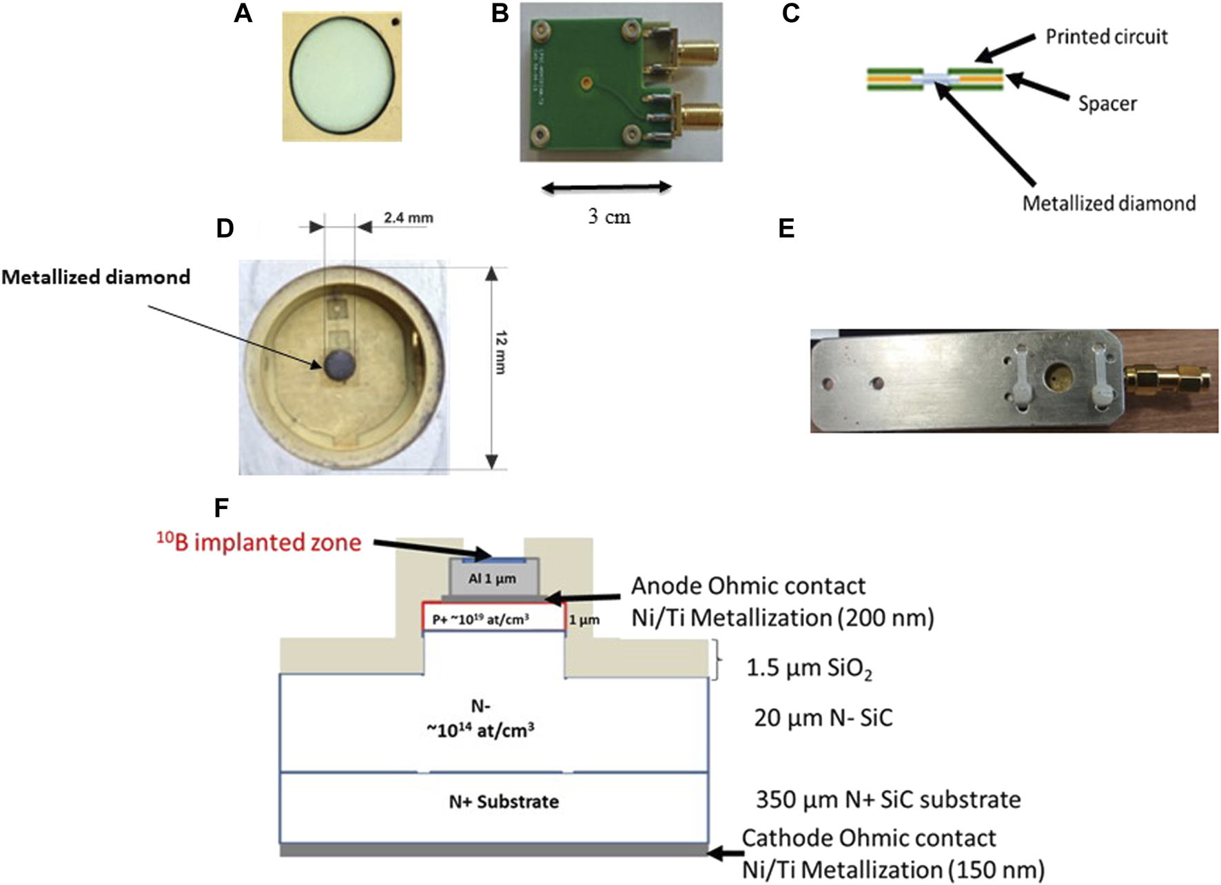
Diamond sensor A with a disk shaped metallization (A) housed in its socket (B) according to the assembly illustrated in (C) (reproduced from [22]), (D) front side and (E) back side of diamond sensor B, 50 µm thick with contacts of 2.4 mm in diameter, (F) schematic representation of the investigated 4H-SiC-based diode.
The IFJ-PAN diamond detector is a sCVD. The detector (labeled with letter B in Table 1) is 2.4 mm wide and 50 µm thick with metal contacts. These metal contacts were manufactured by Diamond Detectors Limited (DDL), as a composition of diamond-like-carbon (DLC), Pt, and Au layers with 3, 16, and 20 nm thickness, respectively. The DLC layer was deposited on the sCVD surface by argon ion sputtering of a graphite target. This approach improves the attachment to the CVD diamond surface1. Deposited on top of the DLC metal layers of Pt and Au act as a quantum mechanical junction, thus electrons are driven from the diamond substrate to the metal layer creating a good ohmic contact. It is worth noting, that the rounded metallic cover visible in Figure 1D has been removed during the measurement in order to study the characterization of the detectors also under tilted position with respect to the beam axis (see Effect of detector tilt angle on fission fragments detection for details).
Detectors A, C, D, E and F (respectively B) were tested intensively at LPSC (respectively IFJ-PAN) or in-beam prior to present experiment at ILL, as reported in the following two paragraphs and in [10, 22].
Characterization at Laboratory
The quality of the contacts was inferred by measuring the leakage current versus applied bias voltage (Figure 2). The curves that correspond to the detectors E and F are relatively symmetrical and exhibit high leakage currents about 10–7 A as soon as the voltage increases up to few hundreds of volts either positively or negatively. For the other detectors, surge of leakage current approaches linear behavior relatively quickly. This is true mainly for detectors A and B which are sCVD diamonds rather than for detectors C and D which are pCVD ones. Due to the supposed ohmic nature of detector B contacts, a more symmetrical behavior would have been expected both for positive and negative bias voltages.
FIGURE 2
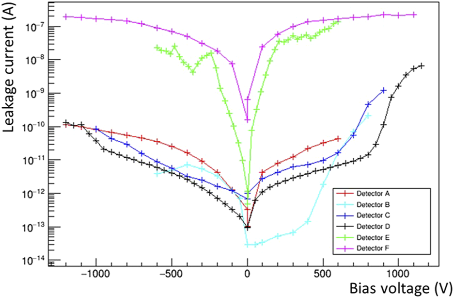
Measurement of the leakage current versus the bias voltage for various diamond samples.
Furthermore, using a241Am 5.5 MeV α source, it was found that detector A exhibits a charge collection efficiency of 100% against 30% for detector C, 32% for detector D and 44% for detector F (see Figure 3 taken from [23]). This last observation is indicative of the density of defects in the crystal structure. Indeed, the XBIC (X-rays Beam Induced Current) tests that we carried out at the ESRF (European Synchrotron Radiation Facility) and reported in Ref. [10] (see X-rays ) demonstrated that the response of C-type pCVD diamonds detectors may vary by a factor 6 of difference between the highest signal response (some few hot spots scattered on the whole surface) and the lowest signal response areas. Such a dispersion in the response on the diamond surface is entirely in favor of the dispersion observed on the distribution corresponding to detector C or D in Figure 3 measured that time on an α source test bench at laboratory. For detector F, which is a heteroepitaxial diamond grown on iridium, while detectors C, D and E are non epitaxial pCVD diamond, large inhomogeneity was observed as well at ESRF on the diamond surface (large extended defect areas—see X-rays and [10])) that explains the poor charge collection with the α source as well. All these results were also confirmed using a focused pulsed beam, a few 10 keV electron beam, weakly penetrating particles, as described in Weakly penetrating electron beam.
FIGURE 3
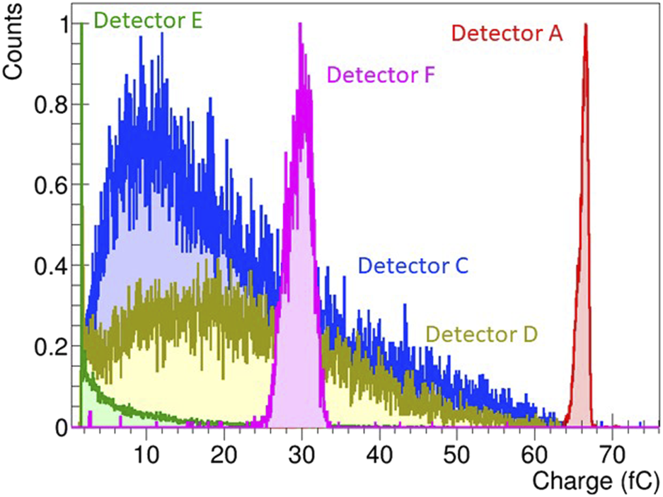
Charge distribution measured using a241Am α source for diamond detectors A, C, D, E and F. The two α energies of the 241Am (5,443 keV and 5,486 keV respectively) cannot be distinguished leading to a single ≈5.5 MeV α peak with a resolution of 1.2% for diamond detector A and a charge collection efficiency of 100% against 30%, 32 and 44% respectively for diamonds C, D and F. Charge collection efficiency on detector E is too poor to be quantified. Diamond detectors were biased at 500 V and electron signal was collected [23].
Finally, it should be noticed that we suspect that diamond detector E is not an electronic grade diamond but an optical grade one, unlike the two other pCVD samples. These considerations may explain the observed differences both in Figure 2 and Figure 3.
Characterization Using Focused Particle Beams
X-Rays
The European Synchrotron Radiation Facility in Grenoble (ESRF) provides on beam line ID21 a focused (∼1 µm) pulsed (100 ps bunch duration, ∼103 photon/bunch) X-ray beam of 8.5 keV, with an almost uniform energy deposition along the irradiated volume in the detector, therefore mimicking the interaction of crossing individual charged particles. The XBIC (X-ray Beam Induced Current) set-up of the ID21 beamline enabled us to draw a 2D response map of disk metallized detectors using a focused micrometric beam with a pitch on the surface at the level of few tens of microns [10]. The charge collection efficiency was measured directly at the output of the diamond material (no preamplifier) by a Keithley 485 picoammeter. Diamond A has shown a very homogeneous response with a charge collection efficiency of 100%. A stripped metallized 10 10 0.300 mm3 pCVD diamond similar to detector C from the same manufacturer Element 6 showed a scattered location of hot spots linked to the spatial distribution of grain boundaries in the polycrystalline material. However, the overall response of the detector is relatively homogeneous, but the charge collection efficiency is poorer than for detector A. Finally, the most important conclusion that has been drawn is that the hetero epitaxially grown F detector showed very large inhomogeneity over the surface, with large areas of very poor charge collection efficiency that may be a sign of charge carrier trapping at dislocation sites. These results corroborate those with a241Am source obtained at LPSC [23, 24].
Weakly Penetrating Electron Beam
In Institut Néel in Grenoble, an eBIC set-up (electron Beam Induced Current) was used to study the performance of the three diamond samples A, C and F with a weakly penetrating beam. Indeed, the 30 keV eBIC penetration has been estimated with the CASINO simulation toolkit [25] to be less than 10 µm from the diamond surface, which is very similar to the one expected for fission fragments (SRIM [26]). A cartography was done for the three aforementioned diamonds (see respectively Figure 4A,B,C). Obviously similar conclusions as for the XBIC test can be drawn, even if the two experiments are very different. For the first, electrons stop close to the surface while for the second, the bunch of 8.5 keV X-rays traverses the crystal, which will deposit about 5 MeV for the diamonds of thickness 517 µm (detector A) and 3 MeV for diamonds of thickness 300 µm (detectors C and F). A qualitative analysis from results exposed in Figure 4A for diamond A shows that the 2D map reflects a very homogenous structure. While in Figure 4B the grey scale enhances a quasi-homogenous distribution of “hot spots” among the surface that reflects the grain boundary distribution in diamond C. Finally, the DOI structure of diamond F, Figure 4C is very inhomogeneous with extended areas with very low response. We can notice notably the area which appears black in the grey scale on the right. Elsewhere on the surface, certain areas of relatively large size range from very bright white with a level of brightness comparable to the surrounding copper ring where the charge collection is made to a much lighter grey. Finally, the scratches on the on the periphery of the metallization disks are due to wear induced by the friction of the copper ring on the metallization.
FIGURE 4
eBIC cartography done at Institut Néel of the three diamond samples: detector A (A), a zoom on a 1 mm2 area of the detector C (B) and detector F (C).
Silicon Carbide Detector
Detector Housing
The SiC-based detectors have been previously developed within the framework of the I-SMART project (Innovative Sensor for Material Ageing and Radiation Testing) involving the CEA and Aix-Marseille University [27].
SiC-based neutron detector consists in a 4H-SiC p+n diode, using a n+-type wafer with a substrate of 350 μm thickness, on which a 20 μm thick n-type (∼2 1014 cm−3 doping concentration) was grown. To create the pn-junction, a 1 μm thick p+ epitaxial layer with a high aluminum doping concentration ∼1019 cm−3 was deposited on the n-type layer. Next the ohmic contact (Ni/Ti) with 200 nm thickness has been deposited by high vacuum electron beam evaporation. In order to reduce the contact resistance, a 1 μm Al metallic contact has been deposited under high vacuum electron beam evaporation on the top of the ohmic contact. Boron-10 was implanted within the metallic contact for realizing a neutron converter layer (5 × 10¹⁵ Atoms cm−2 10B implanted). In the present work the area of the investigated diode was 0.075 cm2. The schematic representation of this diode is illustrated in Figure 1F.
Detector Characterization Under Neutron Flux
These detectors were implemented at MINERVE, a Zero-Power reactor at CEA Cadarache. They demonstrated a better signal-to-noise ratio (peak area to background area ratio) at 0 V detector bias than at - 200 V.
The better signal to noise ratio at 0 V than at −200 V can be explained by the fact that the space charge region is thin (4 μm), and only a very small fraction of the energy is therefore deposited by photoelectrons and Compton electrons in the detector’s active volume.
SiC-detectors showed stable characteristics over 1800 s neutron irradiation at a flux of about 9×10⁸ n cm− 2 s−1 (thereof about one third thermal) [28].
Leakage current for the SiC-detectors was measured to be few nA.
Experimental Set-Up at the LOHENGRIN Mass Spectrometer
Fission Fragments Production and Selection
The LOHENGRIN separator at ILL was used to provide mass- and energy-separated FF. Two 7 0.5 cm2 235U and 233U targets respectively are mounted on a 0.4 mm thick Ti backing and covered by a 0.25 µm thick Ni foil [29]. The 233U target was supplemented by a spot of evaporated 6LiF. As illustrated in Figure 5, the targets are placed at an in-pile position and exposed to a thermal neutron flux of ≈5 × 1014 cm−2 s−1. Thermal neutron-induced fission of uranium isotopes produces a light FF with the mass yield distribution peaking around A ≈ 95 and a complementary heavy FF with the yields peaking around A ≈ 140. Light FF have a kinetic energy distribution peaking close to 100 MeV while heavy FF have kinetic energy distributions peaking at 50–80 MeV depending on their mass. The intrinsic FF energies are reduced by energy loss in the target and the Ni cover foil respectively, thus effectively covering a wider range of energies that can be selected by the spectrometer.
FIGURE 5
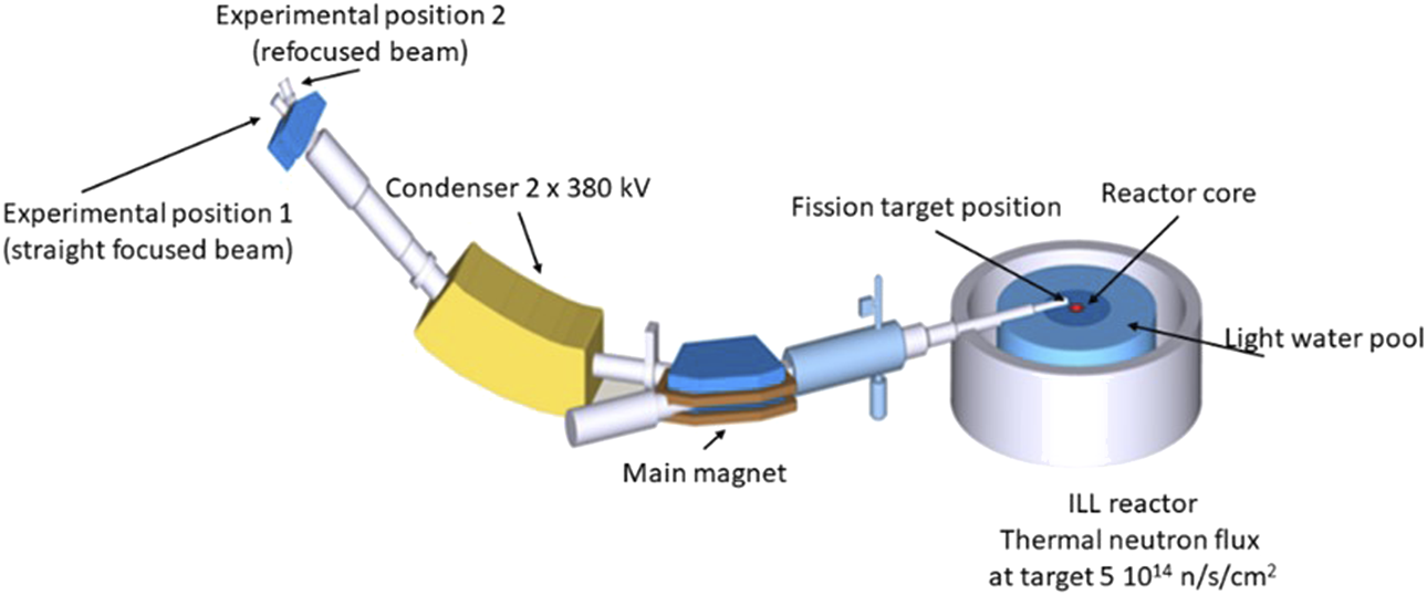
Schematic of the LOHENGRIN spectrometer [29].
The recoiling FF that are typically ionized to charge states Q ≈ 20 are then separated according to A/Q and E/Q by the parabola spectrometer, where A, Q, E are the mass, ionic charge state, and kinetic energy of the FF (see Figure 5). Measurements at LOHENGRIN were carried out with various settings with mass numbers ranging from 84 to 144 and kinetic energies from 35 to 110 MeV in order to determine the characteristics of the detectors over a wide range of energy and mass/atomic numbers. Each scan comprised several runs with varying energy in steps of 5 MeV while keeping mass number and charge state constant. Mass-separated FF from LOHENGRIN are composed of several isobars. For illustration, the average nuclear charge from the JEFF3.3 [30] fission yield database is given for each mass. Tritons and α particles as light ions with lower stopping power were also used for characterization to verify the consistency with the off-line characterization. For this purpose 6Li (n,α)t reactions on the deposited LiF provide 2.7 MeV tritons and 2.05 MeV α particles. The 59Ni(n,α) reaction provides 4.75 MeV α particles where the 59Ni is bred by 58Ni(n,γ)59Ni reactions in the Ni target cover foil of the targets. Moreover, 1.4 MeV α particles are available from the 10B (n,αγ) reaction on boron collimators present in the LOHENGRIN beam tube. Given the thickness of these target materials some somewhat lower particle energies can be selected too with the LOHENGRIN spectrometer. The intrinsic FF energies are reduced by energy loss in the target and the Ni cover foil respectively, thus effectively covering a wider range of energies that can be selected by the spectrometer, 7 cm wide fission targets were used which leads to an energy acceptance of 1.0% of the spectrometer [4]. The energy calibration of the spectrometer is based on (n,α) and (n,p) reactions producing ions with well-known energies. The linearity of the electric and magnetic fields of the spectrometer are controlled by reference resistors and an NMR (Nuclear Magnetic Resonance) probe respectively. Thus the mean energy of ions selected by the spectrometer is known to be better than 0.2%.
Detector Front-End Electronic and Data Acquisition
Transverse dimensions of detectors A and B are different but due to their housing (Figure 1), the two apparent metallized detection areas are similar and equal to ∼2.4 mm2. The main difference arises from the fact that detector A (and detectors C, D, E and F as well) enables reversible bias and signal readout from both sides whereas detector B can be read only on one side. The signal readout of all detectors (diamond and SiC) was performed using preamplifiers.
A low-noise broadband RF amplifier: 2 GHz, 40 dB from CIVIDEC Instrumentation Company [31] (namely CIVIDEC C2) was used in the context of timing measurement and waveform analysis. Concerning data acquisition, it was performed with a 500 MHz bandwidth, 3.2 GS s−1 digital sampling “Wavecatcher” [32] system. The advantage of using this system lies in the fact that it could be configured in a continuous acquisition mode, recording all waveforms, and thus enabling large statistics for offline analysis.
The spectroscopic performances of the detectors were studied with a dedicated low noise and fast response charge sensitive preamplifier developed by INFN. The preamplifier has two channels with charge sensitivity 0.93 (1.77) V/pC, with rise time 1 (2.5) ns, a decay time 100 μs for channel 1 (2), and a maximum output voltage of 4 V. The signal from electron/hole collection side of the detector was connected to each preamplifier channel and then sent to a spectroscopy amplifier [33] with a 0.5 µsGaussian shaping time. The readout acquisition was operated on a dedicated subset version [34] of a VME general purpose DAQ based on a 32-channel 12-bit peak sensing ADC (Analog to Digital Converter) V879 from CAEN [35].
Detector Polarization Effect Handling
A Keithley 6,487 voltage supply, which allows a programmable inversion of the bias, was used to perform voltage inversion cycles. Such a procedure, named “cycling”, was done in order to minimize the significant polarization [12] effect generated over time mainly in the pCVD and DOI diamond detectors. Operating inversion voltages and the transition ramps were controlled by a LabVIEW program developed at laboratory [23] using the following procedure: measurement during 3 min biased at + 450 V then the bias was inverted at −450 V during 1 min with a ramp of 50 V s−1.
Detector Performances as FF-Detector at LOHENGRIN
Optimal Detector Configuration for Short Range Particle Detection
Series of measurements with a light FF of mass 98 (labeled later on FF98 considered as the reference fission fragment) were carried out prior to any detector performance measurement. It was aimed to find out an optimal combination of “face exposed to FF” versus “applied bias voltage”. Figure 6 illustrates the variation of the signal amplitude as a function of the applied bias voltage for detector A when exposed to FF98 at the reference kinetic energy of 90 MeV. Indeed, due to the CVD diamond growth process, the two diamond sides (“growth” for “top” versus “seed” for “bottom”) may exhibit some asymmetries. Furthermore, depending on positive or negative bias voltage applied on diamond material, the nature of the charge carrier, electron versus hole, collected on the electrode differs. That might be a cause of asymmetries as well due to a possible difference in charge trapping in the diamond bulk for electron and holes. In the present paper, the two diamond sides will be later on arbitrarily called 0° and 180° for reasons of clarity. This choice was motivated to avoid any misunderstanding in the conclusion of our analysis given that the two faces were not previously identified in relation to the growth conditions. In Figure 6, the maximum voltage that could be applied to diamond detector A was found to be 450 V. For higher voltages, discharge spikes were observed that might damage the diamond metallization. These observations led us to consider, for future experiments, a new model of detector holder in which the electrical connection is operated more robustly by wire bonding.
FIGURE 6
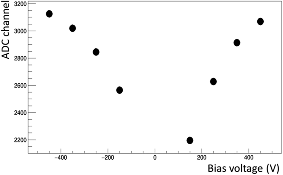
Signal amplitude versus applied bias voltage for 90 MeV FF98. For negative voltage the diamond side 0° was exposed to FF98, on the contrary, for positive voltage the diamond side 180° was exposed to FF98. Error bars are within the point size.
Furthermore, in Figure 6, it can be noticed that the signal amplitude is increasing with bias voltage but, even if the slope of the curves decreases at higher voltage, no plateau is reached. All the measurements carried out with the different detectors confirm this observation. The significant space charge along the incident particle trace generates an electric field in the opposite direction to that applied, increasing local recombination and thus preventing an optimum charge collection. This is in relation with the PHD effect described in Pulse Height Defect.
Detection Efficiency
The detection efficiency here is defined by number of ions detected by candidate detectors divided by the number of incident ions measured with a Si detector which has 100% detection efficiency in the sensitive area. Collimators with sizes corresponding to the diamond detector aperture: 2.4 mm (measured on the detector holder for both sCVD A and pCVD D) and 7 mm (same but for pCVD E) were installed in front of the Si detector. The readout electronic chain was the one used for spectroscopic measurement (Detector front-end electronic and data acquisition). The detection threshold was set above the noise level ∼1 MeV α particles with energies 1.4, 4.5 and 4.7 MeV and FFs of mass 98 (136) with different energy 100, 90 and 80 MeV (77, 70 and 63 MeV) respectively, were used to determine the efficiency.
The loss in the detection efficiency results from incomplete charge collection efficiency of pCVD caused by grain boundaries [36]. The average charge collection efficiency of CVD diamonds vary from 100% (Figure 3) to 5% depending on the diamond detector quality [23]. The loss in charge collection efficiency is maximal for highly ionizing FF since the stopping range of FF is very short (6–8 μm for light FF) while α particles have a longer range (e.g., ∼11 μm for 4.7 MeV) [26, 37].
The sCVD detector A showed ∼102% efficiency compared to the Si detector (see Table 2) where the systematically larger value is probably due to the uncertainty in the collimator geometry. This indicates good charge collection efficiency in all regions of the detector surface.
TABLE 2
| Particle | Energy [MeV] | Efficiency [%] sCVD A | Efficiency [%] pCVD D | Efficiency [%] pCVD E |
|---|---|---|---|---|
| α | 1.4 | 100.6 | — | 32.9 |
| 4.5 | 100.7 | — | — | |
| 4.7 | 102.2 | 81.4 | 31.0 | |
| FF A = 98 | 100 | 101.3 | 82.3 | 29.4 |
| 90 | 106.9 | 86.7 | 36.2 | |
| 80 | 104.5 | 86.5 | 29.5 | |
| FF A = 136 | 77 | 103.1 | 77.2 | 28.1 |
| 70 | 98.0 | 85.5 | 30.2 | |
| 63 | 104.7 | 79.2 | 27.4 |
Efficiency of different diamond detectors with α and FF (A = 98, 136) at different energies.
The pCVD detectors showed lower efficiency compared to the sCVD detector. The small detector D showed ∼83% efficiency. The decrease in efficiency was mainly due to the bias recycling procedure, where the detector was at the nominal bias during 70% of the measurement time (see Detector polarization effect handling), indicating the good charge collection efficiency during the normal bias up to ∼100%.
On the other hand, the 7 mm pCVD detector E showed low efficiency ∼31%, which cannot be explained by bias cycling. This could be due to the low charge collection efficiency of this diamond detector, causing the collected charge falls below the detection threshold (see Table 2).
As previously mentioned, due to the pCVD detector structure (grain distribution), the charge collection depends on hit position on the detector, where efficient charge collection is carried out in region with large grain size, while region between the large grains in the surface shows dead region. This surface effect is enhanced for low energy fission fragment which stops at the surface of the detector ultimately causing the decrease in the efficiency. As the pCVD detector E is an optical grade and not an electronic grade detector, the results are worse than for the detector D.
Spectroscopy
single Chemical Vapor Deposition Performances
In the absence of a plateau in Figure 6 signifying a complete charge collection, an optimum voltage of ∓450 V (side 0° versus side 180°) was chosen for diamond detector A which means a field of 0.9 V μm−1. Similarly, for diamond detector B, an optimum voltage of - 200 V was set. It means an electric field of 4 V μm−1 that is 4.5 times larger than for detector A. As noticed previously, only one side of diamond B can be exposed to FF. It will be called “side 0°” later on in the manuscript.
α Particles and Tritons
At first, the two diamond detectors A and B were exposed to 4.75 MeV α particles and 2.7 MeV tritons respectively. Figure 7B illustrates an energy resolution for diamond detector B of 0.5% RMS with α particles and, in Figure 7E of 0.7% RMS with tritons (blue histogram). Both measurements were done with an incidence angle of 0° (incidence relative to the vertical axis perpendicular to the surface of the detector). Besides, the other histogram plotted in red in Figure 7E is relative to the tritons detection with a detector tilt of −45°. Within fit uncertainty no significant degradation of the resolution is observed. The tilt of the detector effectively increasing the thickness of the “dead layer” (passive material traversed by the incident particle, e.g., top electrode metallization) has only little influence on the energy resolution for diamond detector B. For diamond detector A, the thicker one, an energy resolution of 0.7% RMS was obtained at an incidence angle of 0° both with α particles and tritons (Figure 7A,D). This result is to be compared with the one obtained at LPSC with the 241Am source detailed in Characterization at laboratory and illustrated by Figure 3. In this case, the α rays 5,485 MeV (84.5%) 5,442 MeV (13%) and 5,388 MeV (1.6%) emitted by the 241Am source are mixed in a single peak which leads to a 1.2% RMS [23] estimation for the energy resolution, which is consistent.
FIGURE 7
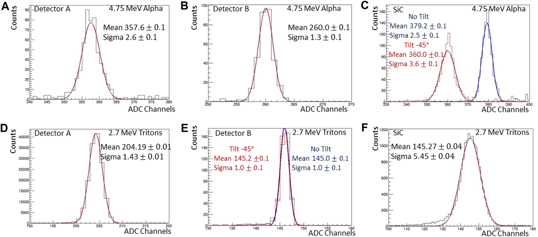
Energy resolution with 4.75 MeV α particles of diamond detectors A (A), B (B) at normal incidence and for SiC both at normal incidence and with a detector tilt of -45° (C). Energy resolution with 2.7 MeV tritons at normal incidence for both diamond detector A (D) and SiC (F) and compared results at normal incidence and with a detector tilt of -45° for diamond detector B (E).
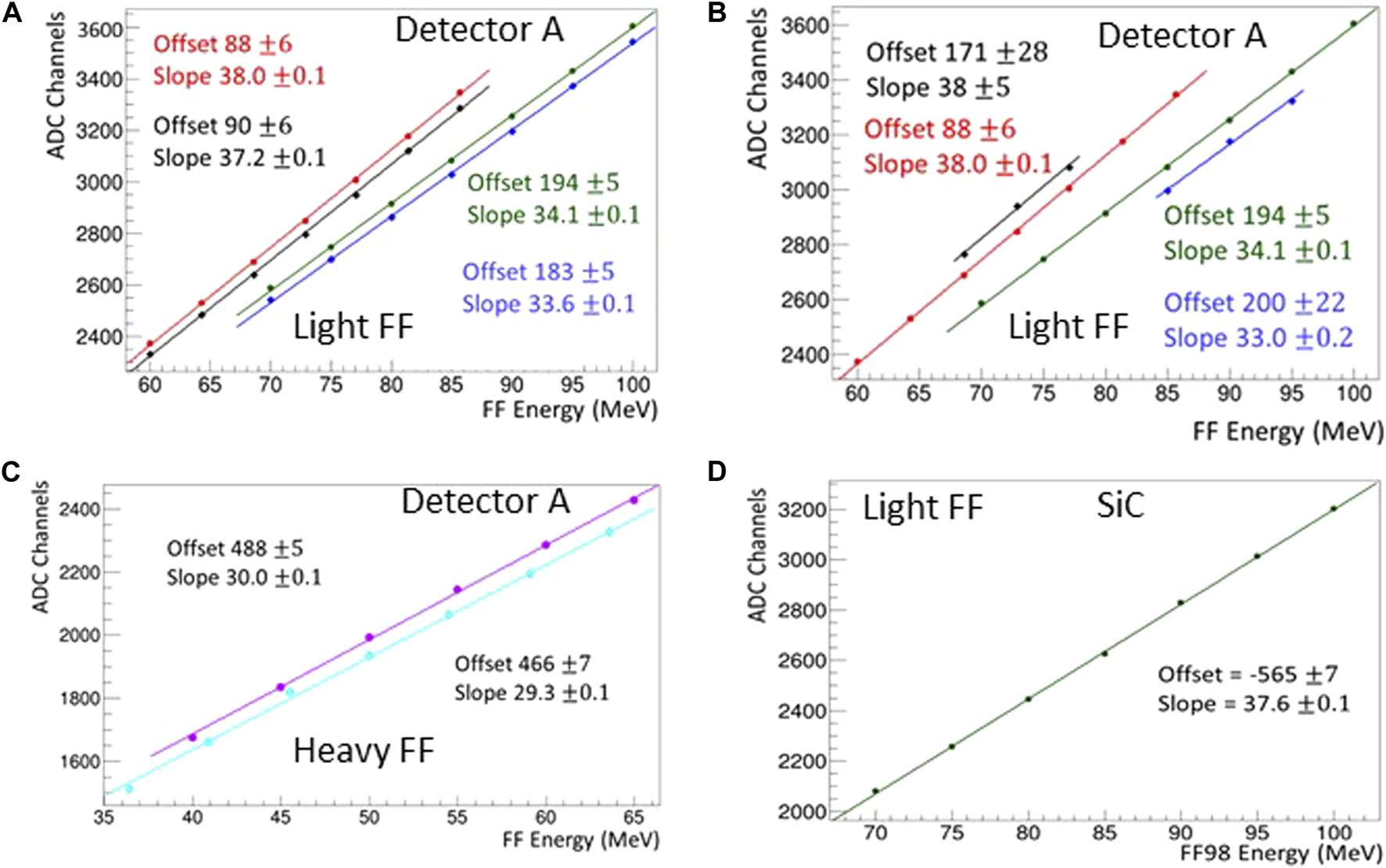
With an incidence angle of 0° for the incoming particles hitting the detector, a linear fit of ADC channel versus energy of incident particles results in the two following formula for detector A, Equation 1, and detector B, Equation 2, in the present experimental set-up:where E is quoted in MeV.
The difference in the calibration coefficient values comes from two different gain settings of the charge preamplifier. This setting was optimized on each of the detectors in order to be able to record the entire energy spectrum of from 2.7 MeV tritons up to 105 MeV light FF in order to allow the study presented in section Pulse Height Defect. As α particles and tritons are expected to show negligible Pulse Height Defect (PHD), indeed in [38] it has been already reported that PHD is almost negligible for protons or α particles for energies beyond several MeV, these formula will permit later on to evaluate the PHD effect of FF spectroscopic measurements.
Fission Fragments
Light Fission Fragments
Diamonds A and B were exposed to FF98 while a ramp in energy from 70 MeV up to 100 MeV was applied by steps of 5 MeV. As with LOHENGRIN fission fragments are separated according to their A/Q and E/Q ratio, for each LOHENGRIN setting, several fragments with different Q may reach the detector. For the run (A = 98, Z ≈ 39, E = 70–100 MeV) two fragments FF98 and FF84 reach the detector. The two detectors A and B gave very similar results. A mean resolution of 1.6% RMS was found for detector A and 1.4% RMS for detector B (10 times thinner) calculated over the whole energy range Table 3 for FF98. Figure 8A,B illustrates the obtained results at a FF98 energy of 100 MeV. As a matter of comparison with an accurate ionization chamber, a FWHM resolution better than 1% is routinely reached [39].
TABLE 3
| Diamond | Fragment | 70 MeV | 75 MeV | 80 MeV | 85 MeV | 90 MeV | 95 MeV | 100 MeV | Mean |
|---|---|---|---|---|---|---|---|---|---|
| sCVD A | FF98 | 1.6 | 1.5 | 1.7 | 1.5 | 1.5 | 1.6 | 1.6 | 1.6 |
| sCVD B | FF98 | 1.4 | 1.5 | 1.5 | 1.3 | 1.3 | 1.5 | 1.5 | 1.4 |
| SiC | FF98 | 4.2 | 3.2 | 3.8 | 3.1 | 3.4 | 3.1 | 3.2 | 3.4 |
| Fragment | 59 MeV | 64 MeV | 69 MeV | 73 MeV | 77 MeV | 81 MeV | 86 MeV | Mean | |
| sCVD A | FF84 | 1.3 | 1.5 | 1.3 | 1.2 | 1.3 | 1.3 | 1.3 | 1.3 |
| sCVD B | FF84 | 1.4 | 1.0 | 1.1 | 1.4 | 1.2 | 1.1 | 1.1 | 1.2 |
| SiC | FF84 | 2.1 | 2.6 | 2.2 | 2.2 | 1.8 | 1.9 | 1.8 | 2.1 |
| Fragment | 40 MeV | 45 MeV | 50 MeV | 55 MeV | 60 MeV | 65 MeV | 70 MeV | Mean | |
| sCVD A | FF144 | 1.9 | 1.5 | 1.7 | 1.6 | 1.3 | 1.0 | — | 1.5 |
| sCVD B | FF144 | 2.0 | 1.3 | 1.7 | 1.4 | 1.3 | 1.6 | — | 1.5 |
| SiC | FF144 | — | — | — | — | — | 6.9 | — | — |
| Fragment | 36 MeV | 41 MeV | 45 MeV | 50 MeV | 54.5 MeV | 59 MeV | 63 MeV | Mean | |
| sCVD A | FF131 | 2.4 | 2.2 | 2.9 | 2 | 1.7 | 1.5 | 1.5 | 2.0 |
| sCVD B | FF131 | 1.8 | 2.2 | 2.4 | 2.3 | 2.4 | 2.0 | 1.3 | 2.0 |
| SiC | FF131 | — | — | — | — | — | 2.2 | — | — |
Summary of the energy resolution (RMS values in %) measured with various detectors on FF98, FF84, FF144 and FF131 at various energies. Bias voltage for diamond detector A is −450 V; diamond detector B is −200 V; and SiC detector is −100 V.
FIGURE 8
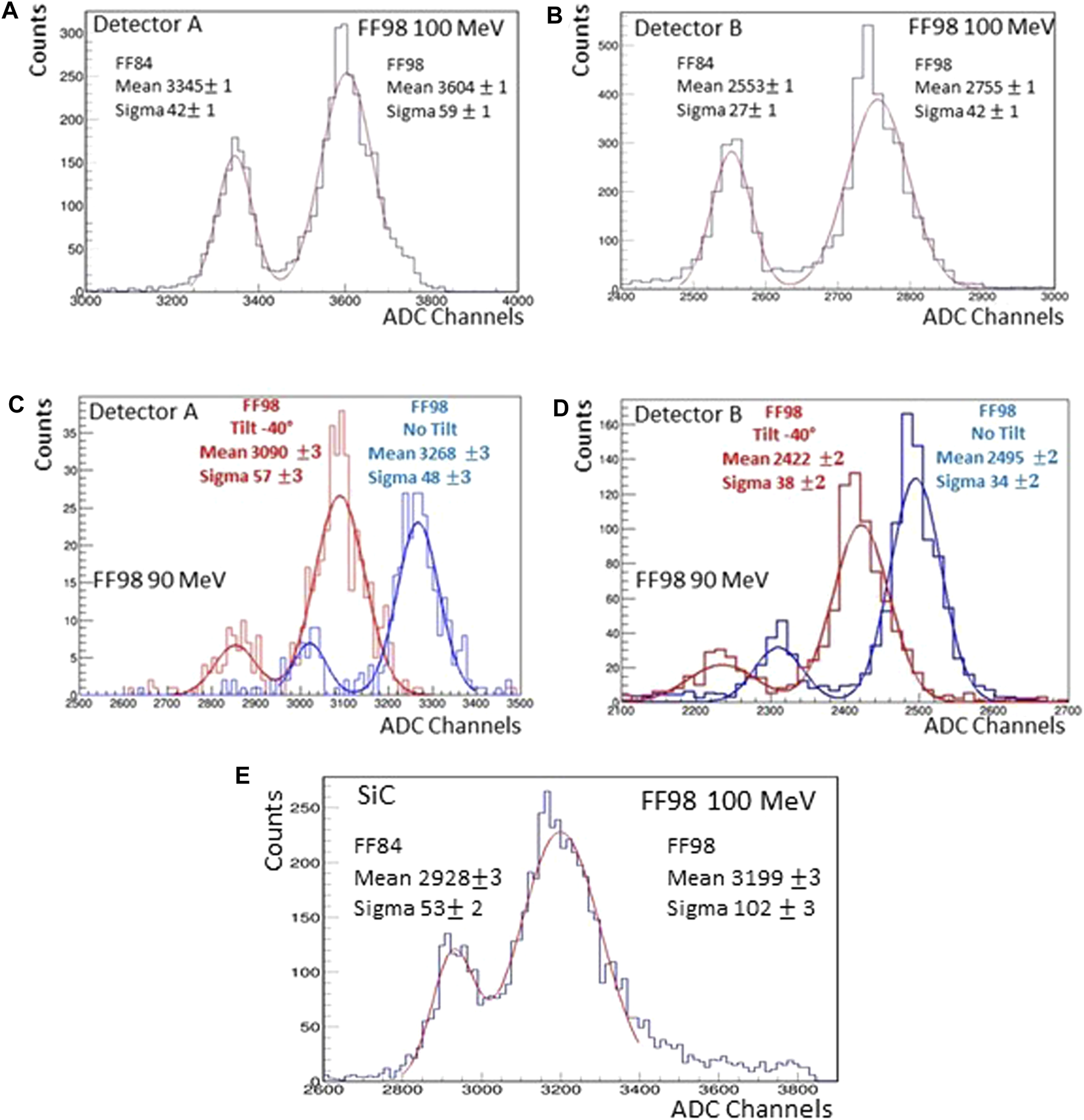
FF98 and FF84 spectroscopic measurement and energy resolution with diamond detectors A (A) and B (B) for energy of 100 MeV for FF98 and 86 MeV for FF84. The diamond A is biased at -450 V, the diamond B at -200 V, and for both side 0° is exposed to FF. Tilt of the diamond detector A (C) and diamond detector B (D) for 90 MeV FF98, the blue curve corresponds to 0°, the red one to a tilt of −40°. The ratio of the two mean values is 94.6% (diamond A) and 97.0% (diamond B), i.e. the pulse height defect increases by 5.4% for diamond A and 3% for diamond B. The FF98 and FF84 spectroscopic measurement and energy resolution with the SiC detector are illustrated in (E). It is biased at -100 V.
The diamond response versus the incoming FF kinetic energy is very linear as it is shown on Figure 9A,B for diamond detector A for both FF98 and FF84. As previously mentioned, for detector A, the two detector sides are read with charge preamplifiers and both signals can be studied. Consequently, two sets of linearity curves are plotted in Figure 9A. Two curves are obtained by analyzing the signal read on side 0° (the one exposed to FF in this experiment) and the two other ones are obtained with the signal read on side 180° (the opposite side). Diamonds are still biased at -450 V. The electron signal is measured. The sets of offset and slope parameters are very consistent, no noticeable difference can be observed, as expected. In the last experiment, diamond detector A is used and at that time the side 180° is exposed to FF. Consequently, the diamond bias is set to +450 V (Figure 6) and that time the hole signal is measured. The linear response of the diamond sensor as a function of kinetic energy of FF98 and FF84 is shown in Figure 9B. Within uncertainties no difference in the slope of the curves for the corresponding FF is observed. A difference in the offset parameter can be noticed mainly for FF84.
FIGURE 9
The ADC peak channel versus incident FF energy is plotted. In (A): diamond A linearity curves are drawn for FF98 (green and blue) and FF84 (red and black). For green and red curves, signal is read on side 0°, whereas, for black and blue curves, signal is read on side 180°. The diamond is biased to −450 V and side 0° is exposed to FF that implies that the electron signal is measured. (B) Green and red curves are the same as in (A), dark and blue differs: FF are now impinging side 180° and diamond is biased to +450 V. That time the hole signal is assessed. (C) Response of detector A to FF131 (light blue) and FF144 (pink), it is biased at −450 V and side 0° is exposed to FF (electron signal). (D) SiC detector linearity curves for FF98, the detector is biased to −100 V (electron signal). For all plots, error bars are within the point size.
Heavy Fission Fragments
Diamond detectors A and B were exposed to FF144 while a ramp in energy from 40 to 70 MeV was applied by steps of 5 MeV. The two detectors A and B give very similar results. A mean resolution of 1.5% RMS was found for FF144 and 2% RMS for FF131 for both detectors A and B (10 times thinner) calculated on the whole energy range Table 3. As observed in Figure 9A,B for light fragments, the diamond response to the energy ramp in Figure 9C is very linear and can be fitted by a straight line like for FF98 and FF84.
Effect of Detector Tilt Angle on Fission Fragments Detection
To evaluate the influence of the orientation angle, several measurements inducing a tilt of −40° with diamond detector A were performed. Results are presented in Figure 8C. The ADC channel difference for the peak centroid (−40° versus 0°) is around 200 channels (∼3 MeV according to Equation 1) which is too large to be explained by the increase of the effective thickness of the electrode aluminum metallization due to the tilt. Indeed, the metallization is 50 nm thick, such that FF is expected to deposit about 500 keV at 0° which results in an increase of 150 keV of deposited energy at 40°. The measured 3 MeV is 20 times higher. It may indicate an additional “dead zone” within the diamond layer as already observed in [40, 41]. It was found that Element 6 diamonds are likely to have a dead layer of about 200 nm at the surface (∼3 MeV loss by FF98). While it was much smaller in DDL detectors. Indeed, for diamond detector B, the same experiment points to a much smaller difference around 70 channels Figure 8D. Furthermore, it has been checked for both detectors A and B that a tilt of +40° leads to an identical shift as the tilt to −40°.
poly Chemical Vapor Deposition Performances
The pCVD diamond sample C was exposed successively to different ions, each time for a 2 hours duration: 2.7 MeV triton, 4.75 MeV α, 90 MeV FF98, and 50 MeV FF144. The diamond detector was biased at -450 V and side 0° is exposed to FF. The results obtained with 90 MeV FF98 are illustrated in Figure 10A. A cycling operation was implemented on the supply voltage, as described in Detector polarization effect handling, to improve the charge collection. No peak can be distinguished in the spectrum. It confirms the results obtained at the LPSC laboratory with the 241Am source illustrated in Figure 3 and results from [42]. The inhomogeneity of the surface response of the detector, we reported in [10] and illustrated as well in Figure 4B, reveals a variation within a factor 6 [10] depending on the impact position on the detector surface. This explains the observed great dispersion. Detector D and E were tested as well but only with FF98 at 90 MeV for a 1 hour duration, corresponding results are illustrated in Figure 10B,C, they exhibit very similar shapes as the ones obtained in Figure 3.
FIGURE 10
ADC counts histograms obtained for a single run while diamond C (A), D (B) and E (C) were exposed to 90 MeV FF98. Diamond detectors were biased at −450 V and side 0° was exposed to FF. Its smaller size explains the difference in statistics for detector D. The run for diamond C is twice longer in time than the ones with D and E.
Spectroscopy measurements with the DOI detector F were carried out, but they unfortunately proved to be unusable for the analysis due to a problem that occurred with the target during the experiment.
As a result of [10], observed difference between pCVD measurements and sCVD ones (Figures 8A,B), may come from the type and the density of defects (grain boundaries size, dislocation distribution, etc.) in the diamond bulk and is linked to growth conditions.
Silicon Carbide Performances
The SiC detector was exposed successively to 2.7 MeV tritons and 4.75 MeV α particles (see Figures 7C,F), FF98 at energies ramped from 70 to 100 MeV and finally to 65 MeV FF144. In the three cases, the detector was biased at −100 V.
For α particles an energy resolution of 0.7% was reached against 4% for tritons Figure 7F. The observed difference in detector tilt with α particles on Figure 7C (0° and −45° are compared) is consistent with the huge thickness of the Al electrode (1 µm to be compared to at most 100 nm for diamond detectors). In order to observe the triton signal, the gain of the charge preamplifier was set to its maximum. These two measurements permit as well detector calibration as expressed by Equation 3 which was obtained similarly to Equations 1, 2:For the run [A = 98 E = 70–100 MeV] both fragments FF84 and FF98 were isolated in the data Figure 8E and the linear response of the detector is illustrated in Figure 9D. The energy resolution was found to range from 3.1 to 4.2% for FF98 and from 1.8 to 2.6% for FF84 on the whole energy interval Table 3. These results are worse by a factor of ∼2 if one compares with that obtained on the previously tested sCVD diamond detectors. Finally, in the case of FF144, it was rather impossible to separate FF131 from FF144 as it was done for sCVD. Therefore, no energy resolution could be fitted.
It should be noticed at this point, that the initial settings to obtain the tritons signal resulted in a saturation of the acquisition system for recording FF data. Consequently, they had to be modified to obtain the results presented in Figure 8E and Figure 9D. and a direct comparison allowing in particular the calculation of the PHD in Pulse Height Defect will therefore not be possible.
Summary
In Table 3 a summary of the measured energy resolutions is reported. The results are expressed in percent for the RMS value. They were calculated at the different energies used during the tests. In the last column, the arithmetic mean is given. In fact, where the resolutions are the least good for a given fragment, this turns out to be a problem of statistics on the batch of events available to carry out the measurement. The results obtained for sCVD A and B (10 times thinner) are quite similar and no significant dependence on the energy of the fission fragment can be observed. In the two aforementioned cases, the resolution obtained with the SiC detector is twice larger.
Pulse Height Defect
Detection of ionizing particles with high energy loss in solid state detectors may lead to a pronounced pulse height defect (PHD) [38, 43–47], which is defined as the energy difference ΔE between the kinetic energy Ek deposited by an incident ion impinging the detector and the apparent energy EDD derived from the measured electric signal [38]:where EDD = Nq Eeh (Nq is the number of collected charge carriers and here Eeh=13.6 eV is as defined before the energy to produce electron-hole pairs in diamond [6, 7]). Up to now, detailed studies of PHD were performed mainly for Si detectors, less for diamond detectors [38].
The established Equation 2, derived from α and triton spectroscopic measurement on detector B gives the value of the expected ADC channel as a function of the kinetic energy. It was evaluated on particles that are not sensitive to the PHD, as explained in α particles and tritons. Using Equation 2 for FF, one would expect, if all the charges deposited by the incoming FF are collected, that the FF98 peak at the energy of 100 MeV measured at channel 2755 in Figure 8B, would be measured in fact at channel 5594 (out of range of the 12 bit ADC set-up). The difference is 2839 channels. That indubitably means that about 50% of the deposited kinetic energy is not detected. This observable attests to the PHD which means that the energy derived from the measured electric signal is different from the kinetic energy deposited by the incident ion. For detector A this difference is equal to 48%.
The electric bias for detector A was at the level of 0.9 V μm−1 against 4 V μm−1 for detector B. It is well known for semi-conductor detectors that space charge effects are reduced when higher electric fields are applied. This is illustrated by Figure 6, but one should notice in addition that with FF there is no saturation of the signal amplitude when the bias increases as it can be observed in the literature with α particles [23]. It means that the PHD is never cancelled. Furthermore in the present experiment, the thickness of detector A is 10 times larger than detector B, which favors charge trapping on the path to their collection by the electrodes deposited on both sides of the diamond. Consequently, one might expect a better result for detector B. However, the measured PHD is identical on the two diamond detectors. This shows that the electric field, for the two tested detectors, does not play a major role on the recombination during the charge drift toward the electrodes.
Ions deposit a maximum of their energy at the end of their path, in the Bragg peak. In the present case, given the energy transported by the ions, this will lead, very locally, to a very large amount of charges that will be generated. Taking into account the differences between detectors A and B, as detailed above, which did not lead to differences in the experimental observables for the PHD, we can therefore reasonably assume that the proportion of missing charge comes from in-situ recombination in the region of the Bragg peak.
On the other hand, what is paradoxical in our results is that, in addition, we observe a linear variation of the collected charge compared to the energy of the incident FF at given FF (Figure 9) over an energy range of 70–100 MeV for FF98. When the energy of the FF increases, its depth of penetration, and therefore the position of the Bragg peak in the material, increases also. However, the energy loss rate per unit of FF path length is quite smaller than it is in the region of the Bragg peak where the FF stops. The results of Figure 9 would therefore imply that the Bragg peak occurs at the same FF degraded energy, regardless its initial value, and energy loss at the Bragg peak depends on FF mass. Experiments with a heavier FF (FF144) in a lower energy range, from 40 up to 65 MeV, lead to the same observations. Other conclusions could have been drawn if it had been possible to go below 70 MeV for the light FF, but this was not possible in this case.
For a better understanding, another experiment was done with diamond detector B in the same conditions. One should notice that the difference is that the gain is set to a factor 1.7 lower on DAQ than for previous measurements. A set of FF were selected by LOHENGRIN: 84, 93, 98, and 102 for the light fragments with a range in energy from 70 MeV up to 105 MeV by step of 5 MeV. As well, FF 132 and 144 were selected with energy ranging respectively from 59 MeV up to 78 and 46 MeV up to 65 MeV by steps of 5 MeV. Linear fits of ADC channels versus kinematic energies were done for each FF. The results are plotted in Figure 11A.
FIGURE 11
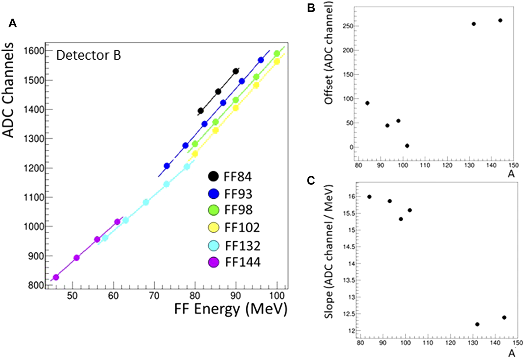
(A) ADC channels versus incoming fragment kinetic energy for a set of FF selected with LOHENGRIN (diamond detector B). The offset (B) and slope (C) parameters as a function of the ionic mass A of incoming FF on diamond detector B surface 0°. The bias voltage is -200 V. Error bars are within the point size. The observed dependency in (B) and (C) for light FF seems to be complex since the corresponding point for FF98 stands out in the two distributions and seems to exclude a purely linear dependency as reported in [5] for silicon detector operated at LOHENGIN in very similar experimental condition.
In Figure 11B,C, the offset and slope fit parameters found for each FF are plotted as a function of the FF mass. An interdependence has been demonstrated. It seems difficult to connect with a smooth curves the measurement points for light FF and heavy FF mainly for Figure 11B (offset parameter). Nevertheless, it can be concluded that, the mass A, and respectively the nuclear charge Z of the incident FF, influences the PHD (note here that FF are selected over their Q parameter, and not Z).
This dependency seems to be complex even if we consider separately the light FF (four data points) from the heavy FF (two data points).
For light FF, in Figure 11B,C, the FF98 corresponding point stands out of the two distributions. It seems to exclude a purely linear dependency as reported in [5] for silicon detector operated at LOHENGIN in very similar experimental conditions. The main difference may arise from the fact that in [5], the silicon detector is a ΔE-E telescope detector device. The combined measurement of energy loss in the thin layer (ΔE) that the FF crosses and in the thicker layer (E) where it stops, improves strongly the FF identification.
The large difference in Figure 11B between light and heavy FF could suggest that, since the energy range in which we have taken these measurements for heavy FF is lower than for the light FF, the offset parameter is more sensitive than the slope parameter, to the incident FF energy. Indeed, there are some evidence of a “dead detector thickness” in Figure 8C (detector A) and Figure 8D (detector B) at the entrance under the metallization layer which creates an offset in the charge collection.
To conclude, as in [38], it appears from the present study that the PHD is to be explained in the framework of recombination models. For heavy ions, such as FF, the main source appears to be the recombination of electron-hole pairs in the plasma bulk produced by the FF when it stops. This theory was first proposed by [48]. As demonstrated in the present analysis, this process is not easy to characterize. It may depend on such factors as energy and intrinsic parameters of the incident FF (A, Z and Q), the applied bias voltage (the maximum electric field investigated here was 4 V µm−1) as well as the distribution of recombination and trapping centers in the detector. There is an indication, with the tilt experiment, of some localized “dead zone” close to the surface, which would not be in favor of an optimal charge collection.
Timing
Diamond detectors are expected to be fast responding detectors. Consequently, a procedure was established to determine the time resolution of the FF detectors, based on off-line analysis of signal waveforms recorded with the Wavecatcher test bench. Actually, no coincidence between two detectors is possible here. Therefore, the timing resolution can be inferred only by comparing the timing difference from the signals of the two detector sides, whenever possible [24].
A numerical Constant Fraction Discrimination (CFD) was performed by averaging the background on the waveforms, determining the maximum of the pulses, and interpolating the 50% rise time value. The time difference measured between side 0° and side 180° on diamond detector A biased at −450 V is equal to 10.2 ps RMS (Figure 12A) which is the best value ever obtained on diamond to our knowledge. A comparable measurement done with detector C (pCVD) lead to a time resolution of 23.8 ps RMS against 34.1 ps RMS for detector D (pCVD) and 16.8 ps RMS for detector F (DOI) which is nearly as good as the sCVD results despite the observed inhomogeneity in charge collection (see Characterization using focused particle beams and [10]). For the three diamonds mentioned last, a cycling operation was implemented on the supply voltage as described in Detector Polarization Effect Handling to improve the charge collection. No timing resolution was evaluated with detector E due to its too poor charge collection efficiency which makes it not a good candidate for our applications. No measurement were done as well with detector B or the SiC detector but for technical reason linked to detector housing.
FIGURE 12
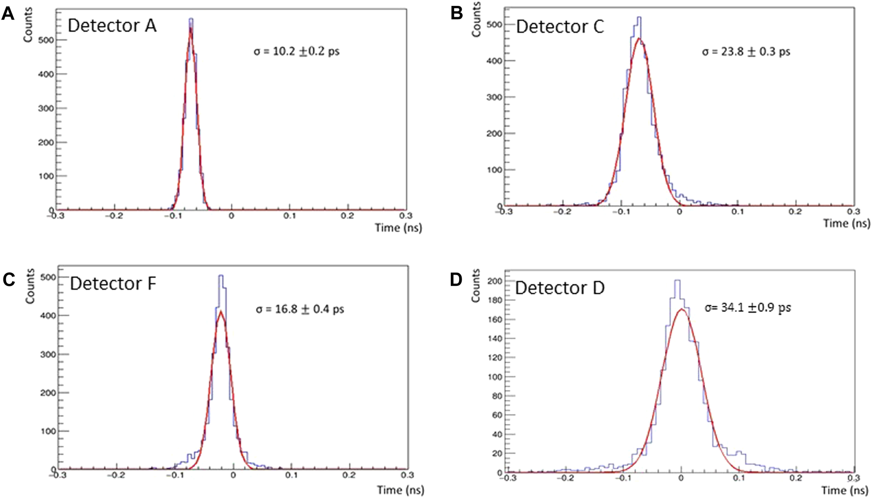
Time resolution (RMS) measured on sCVD diamond detector A (A), pCVD diamond detectorc C (B) and D (D) and the DOI diamond detector F (C) with FF98 at 90 MeV kinetic energy impinging on the detectors under 0⁰. The time value corresponds to the difference in time from the two signals extracted from each side of a single detector after preamplification.
Issue of Integration of Diamond and Silicon Carbide Detectors as FF-Detectors for In-Beam Use
A FF detector used in-beam for thermal neutron-induced fission combined with prompt γ-ray spectroscopy has to satisfy certain criteria, namely in terms of (n,γ) background and neutron scattering, count rate capability, detection efficiency, energy resolution, time resolution, fragment stopping, etc. In the previous section, we reported on a series of measurements to evaluate diamond and SiC detector performances for FF detection at the LOHENGRIN mass spectrometer. Due to the measured performances, we will now consider to what extent and in which possible arrangement this type of detectors could be used in-beam and more precisely in the FIPPS instrument.
Fission Product Prompt γ-ray Spectrometer Experimental Set-Up and FF-Detector Envisaged Configuration
The FIPPS experiment can be divided schematically (Figure 13) into blocks. On the periphery of the instrument, the detector block is equipped with High Purity Germanium (HPGe) detectors (in blue in Figure 13) that allow the measurement of the γ rays emitted during the reactions taking place within the target (in red in Figure 13) chamber. These high-resolution detectors are arranged around a sphere to maximize geometric detection efficiency. Then, the collimation unit part in front of the target cell that delivers a shaped beam of thermal neutrons leaving the guide towards the target chamber. The beam stop block (called beam stop hereafter): this part makes it possible to stop the neutrons passing through the target without interactions. It is located at the rear of the instrument. Finally, the sample environment block, that is located in the center of the instrument, in the middle of the detection system. The sample environment is the site of interactions between neutrons and the target. Depending on the physics cases of interest, the targets can be stable or radioactive.
FIGURE 13
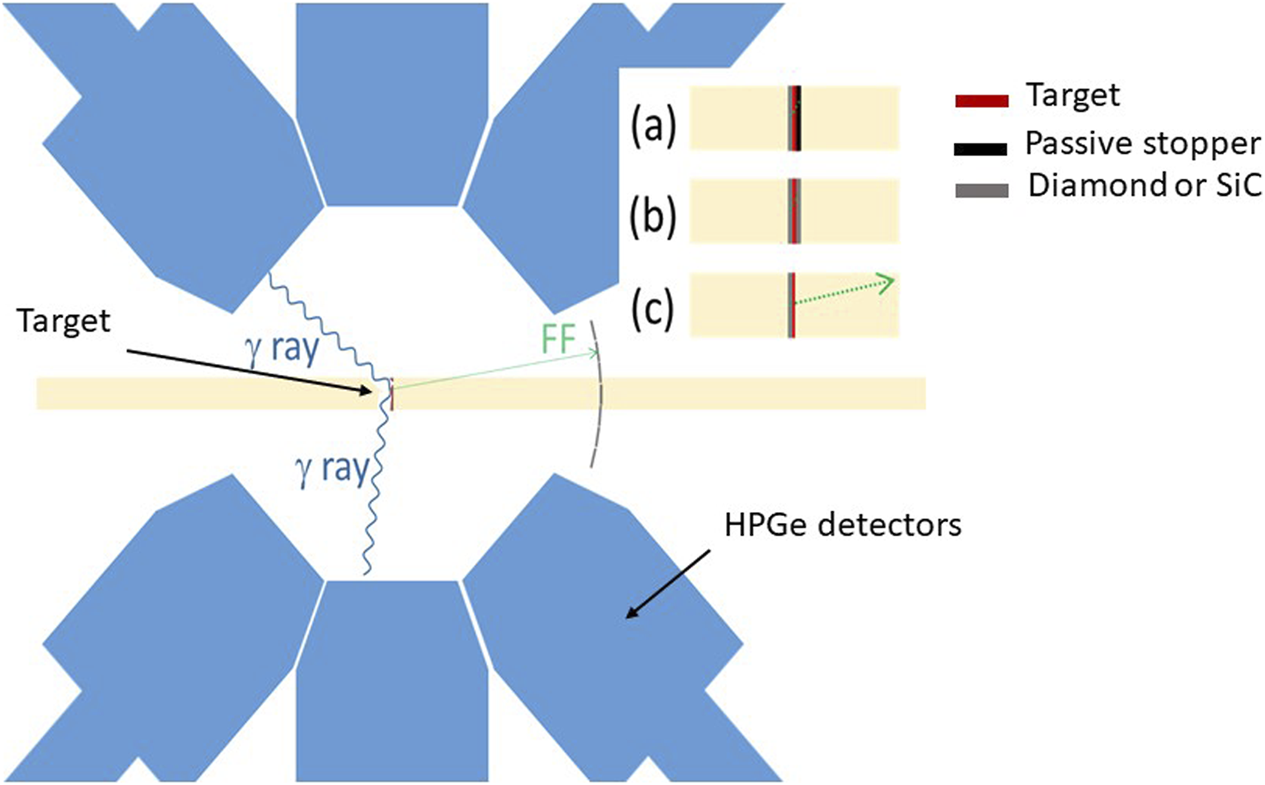
FIPPS detector schematic. Three possible configurations for a target (red) and FF detector (grey) arrangement. (A) Single-sided FF detection with a passive stopper (black) on the opposite side. (B) Double-sided FF detection. (C) Single-sided adjacent FF detector plus a distant FF detector wall on the opposite side.
In the context of the present study, Figure 13 illustrates three possible configurations for a target (red) and FF diamond or SiC detector (grey) arrangement: (a) single-sided FF detection with a passive stopper (black) on the opposite side, (b) double-sided FF detection, (c) single-sided adjacent FF detector plus a distant FF detector wall on the opposite side. These configurations will be discussed now with regard to FIPPS expected performances versus diamond and SiC FF detectors measured performances.
Optimization of the “FF Detector—Target” Configuration
Count Rate Capabilities
The typical fission rate expected is of the order of 100 kHz. Correspondingly, a single-sided FF detector covering 2π solid angle should be able to cope with a FF rate of the order of 100 kHz and a 4π detector would see a FF rate of 200 kHz, pairwise emitted back-to-back. However, some actinide targets have also a considerable self-activity due to their α decays.
Detection Efficiency
Ideally, the FF detector should cover the entire surface of the fission target. This will assure in direct contact nearly 2π solid angle coverage and given that FF are always emitted pairwise back-to-back, a single detector could already provide close to 100% geometric detection efficiency. Only the tiny fraction of FF that are emitted exactly parallel to the target plane or under very small angles to it would be stopped within the target and could not be detected. The active area of the detector should at least match the target area or be larger. Inside the target area the detector should reach close to 100% detection efficiency. This could be realized with sCVD diamond detectors in an edgeless mosaic arrangement or at least with minimum dead layers at the borders. For pCVD, which can have high intrinsic efficiency, a loss in useful duty cycle has to be considered due to bias voltage cycling.
Energy Resolution
A simulation has been performed to determine the energy distributions of FF leaving actinide targets of different thickness, see Figure 14. The calculation was performed for 235UO2 emitting back-to-back a pair of FF 84Ge+150Nd (+2 neutrons, not considered here) as an extreme mass split where the heavy FF has particularly low range, see Figure 14 and Figure 15 respectively. The kinetic energies 84Ge were sampled from a Gaussian with 98.5 MeV average energy and 12 MeV FWHM, and those of 150Nd were matched to satisfy momentum conservation. Homogeneous and isotropic emission from the entire target layer was considered and energies of fragments leaving the target layer through the front or backside of the target were registered. With increasing target thickness a larger fraction of FF gets considerably slowed down in the target and could drop below the detection threshold of an adjacent FF detector. This effect is more pronounced for heavy FF which start out with lower kinetic energies. Thus Figure 15 provides the strongest constraint for the selection of the target thickness. Let’s assume a minimum detection efficiency of 90% is required for single-sided detection of heavy FF and a FF detector with a threshold as low as 10 MeV and negligible pulse height defect (PHD) can be used. Then a maximum target layer thickness of 0.56 mg cm−2 can be tolerated. However, would the detector show 50% PHD for FF, then the latter have to leave the target with the double energy to provide a 10 MeV equivalent electronic signal. This limits the target layer thickness to only 0.4 mg cm−2. For the heavier actinides with significant α activity the probability of α pile-up rises and a higher energy threshold has to be employed to assure clean separation of FF from α particles. Considering a threshold of 20 MeV α-equivalent energy and 50% PHD that corresponds to the results of the present paper for sCVD diamond material, the maximum target layer thickness would drop to only 0.18 mg cm−2. If however both fragments should be detected in opposite detectors with a coincidence efficiency of at least 90% for extreme mass splits, then the corresponding maximum target thickness drops to 0.46 mg cm−2 for PHD-free detectors and 10 MeV threshold, or to 0.28 mg cm−2 for the same threshold with 50% PHD. Comparing these maximum target thicknesses with the required actinide mass in Table 4 (cross-sections and half-lives were taken from [49]) shows that for optimum performance 233,235U and 239Pu targets should be spread out over 2 cm2 while 245Cm and 249Cf may operate with about 1 cm2 target area. Whenever possible a wider spreading of the target mass to reach considerably thinner target layers is strongly preferred. Taking into account the size of commercially available sCVD detectors, a mosaic of at least four individual detectors would be required to cover the entire source.
FIGURE 14
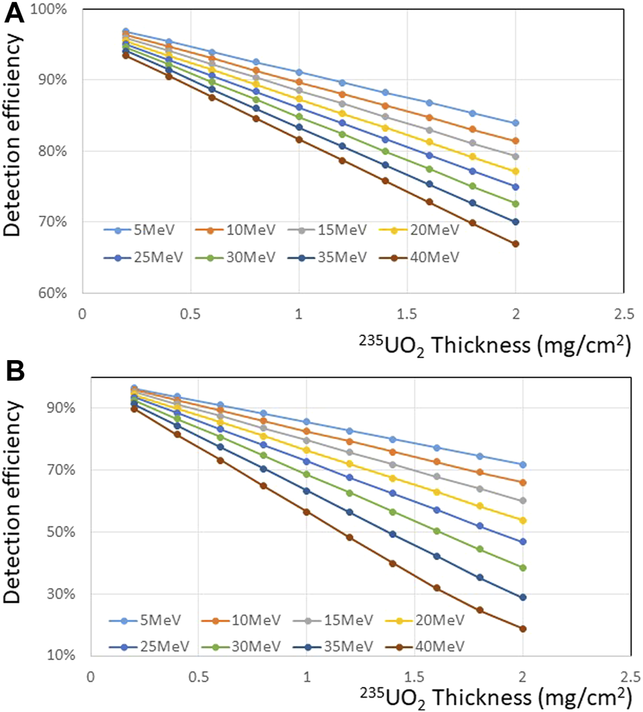
Detection efficiency as function of the 235UO2 target layers of 0.2–2 mg/cm2 thickness. (A) for 84Ge, (B) for the complementary 150Nd.
FIGURE 15
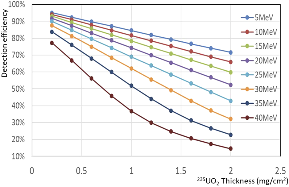
Detection efficiency for simultaneous detection of a pair of 84Ge and 150Nd FF emitted back-to-back, both leaving 235UO2 target layers of 0.2–2 mg/cm2 thickness and both depositing energies above the given threshold in the respective detector.
TABLE 4
| Target | σ(n,γ) | σ(n,f) | M(actinide) | Aα |
|---|---|---|---|---|
| (b) | (b) | (mg) | (MBq) | |
| 233U | 46 | 530 | 1.05 | 0.4 |
| 235U | 99 | 583 | 0.96 | 0.0 |
| 239Pu | 269 | 748 | 0.76 | 1.8 |
| 241Pu | 362 | 1,011 | 0.57 | (2,176 β) |
| 241Am | 720 | 3 | 0.01 | 1.7 |
| 245Cm | 369 | 2018 | 0.29 | 2.2 |
| 249Cf | 497 | 1,642 | 0.36 | 58 |
| 251Cf | 2,850 | 4,895 | 0.12 | 64 |
Properties of different actinide fission targets (cross-sections and half-lives were taken from [49]). The target mass required to reach a fission rate of 100 kHz in a thermal neutron flux of 7·107 cm−2s−1 and the typical associated α activity (also including other isotopes for commercially available enrichment levels). For 241Pu the beta activity is given instead.
241Pu is not decaying by alpha emission, but by beta- emission. The corresponding number of beta activity is shown in italic.
Time Resolution
A good timing resolution, like the one exhibited by diamond materials, would enable a mass determination of the FF via a time-of-flight (TOF) measurement combined with an energy measurement. In this so-called E-v method, both the velocity and the kinetic energy of one fragment are measured to calculate its mass. Thus, the second detector has to be moved away from the target Figure 13C to leave enough flight distance for a meaningful determination of the TOF. The first detector remains in contact with the target to detect the complementary FF and provide a “prompt” timing signal acting as start of the TOF measurement. This method enables a direct determination of the mass M1 of the flying secondary FF, thus the mass M2 of the stopped FF can be determined within the uncertainty of emitted prompt neutrons δν. Since M1 is determined by M1 = 2 E/d2 TOF2, an energy resolution of, say, 1.5% should be matched with a TOF resolution better than 1% so that the experimental mass uncertainty is not higher than the irreducible uncertainty δν. Also somewhat reduced energy and time resolutions remain useful to provide a significant mass resolution. This could be realized with different detector types and distances. For example, with a time resolution of 50 ps per detector the stop detector array should be at a distance of at least 6 cm with 0.5 cm individual detector size to limit angular dispersion in the TOF distance. The time resolution of the SiC detector has not been measured in the present experiment. However, we refer to a recent study where a time resolution of σ 100 ps has been achieved with minimum ionizing β particles in a 55 mm2 4H-SiC detector [50]. While this appears at first glance, one order of magnitude worse than the best value obtained here with diamond detectors (Figure 12A), one needs to consider the correlation of deposited energy and time resolution [24]. FF would deposit several orders of magnitude more energy in such a SiC detector than β particles and thus lead most likely to a considerable improvement of the time resolution. Thus, a combination of a sCVD diamond start detector and an array of 55 mm2 SiC stop detectors at about 6 cm distance could provide sufficient mass resolution for this purpose. Note that in the E-v method the energy loss in the target layer plays no role for the final mass resolution provided the stop detector has a constant relative energy resolution. Fragments that lost significant energy in the target will then simply be slower, even facilitating the TOF measurement.
Conclusion and Outlook
A dedicated experiment to characterize diamond and SiC detectors with mass- and energy-separated fission fragment beams was carried out with the LOHENGRIN spectrometer at ILL. Among the tested detectors, sCVD diamond detectors exhibit the best spectroscopic properties for FF detection. A RMS energy resolution of ∼1.4% was achieved for a 50 µm thick sCVD diamond detector of biased at—200 V for A = 98 FF at 90 MeV energy against 3.4% RMS for a SiC detector. In addition, an excellent time resolution RMS ∼10.2 ps was measured with the same A = 98 FF at an energy of 90 MeV. However, similar to other solid state detectors, also the sCVD detector is affected by a significant Pulse Height Defect which leads to a loss of almost 50% of the initial generated charge carriers, weakly depending of the applied electric field (up to 4 V µm−1) and detector thickness in the range 50 µm up to 500 µm. The pCVD detectors exhibit poor spectroscopic performances, but still excellent time resolution (23.8 ps RMS and 34.1 ps RMS were measured on two different samples from two different manufacturers). Consequently, three different configurations were envisaged that would satisfy diamond and SiC measured performances for a detector integration in FIPPS intended for the study, in nuclear physics, of the structure of neutron-rich fission fragments. A dedicated experimental set-up for detector housing is currently under development and will be tested in the FIPPS context at ILL in a near future.
Statements
Data availability statement
The raw data supporting the conclusions of this article will be made available by the authors, without undue reservation.
Author contributions
All authors have contributed to the instrumental, experimental, or simulation work that has led to the contents of this article. MG-M and YK are the main writers of the text. All authors have contributed to the amendments of the text. They gave their consent on the final version.
Funding
This work was supported by the Labex PRIMES (ANR-11-LABX-0063), IDEX Université Grenoble Alpes (DIATEL project)France and by National Science Centre, Poland, Projects No. 2020/39/D/ST2/03510.
Acknowledgments
The authors are grateful to Matthias Schreck from Augsburg University and Martin Fischer from Audiatec-Augsburg for providing the LPSC laboratory with DOI samples. Dominique Breton and Jihanne Maalmi from LAL-Orsay and Eric Delagnes from CEA Saclay are thanked for their implication in dedicated software development and technical support of the Wavecatcher data acquisition system.
Conflict of interest
The authors declare that the research was conducted in the absence of any commercial or financial relationships that could be construed as a potential conflict of interest.
Publisher’s note
All claims expressed in this article are solely those of the authors and do not necessarily represent those of their affiliated organizations, or those of the publisher, the editors and the reviewers. Any product that may be evaluated in this article, or claim that may be made by its manufacturer, is not guaranteed or endorsed by the publisher.
Footnotes
1.^Contacts on diamond A Galbiati United States Patent 8,119,253
References
1.
JentschelMBlancAde FranceGKösterULeoniSMuttiPet alEXILL-a High-Efficiency, High-Resolution Setup for γ-spectroscopy at an Intense Cold Neutron Beam Facility. J Inst (2017) 12:P11003. 10.1088/1748-0221/12/11/P11003
2.
KandziaFBelierGMichelagnoliCAupiaisJBaraniMDudouetJet alDevelopment of a Liquid Scintillator Based Active Fission Target for FIPPS. Eur Phys J A (2020) 56:207. 10.1140/epja/s10050-020-00201-0
3.
KimYHThomasMFaustHMichelagnoliCKösterUKandziaFet alDevelopment of A Gas Filled Magnet for FIPPS Phase II. Nucl Instr Methods Phys Res Section B: Beam Interactions Mater Atoms (2020) 463:269–71. 10.1016/j.nimb.2019.05.022
4.
ArmbrusterPAsgharMBocquetJPDeckerREwaldHGreifJet alThe Recoil Separator Lohengrin: Performance and Special Features for Experiments. Nucl Instr Methods (1976) 139:213–22. 10.1016/0029-554X(76)90677-7
5.
SinghATopkarAKösterUMukhopadhyayPKPithawaCK. Performance Study of an Integrated ΔE–E Silicon Detector Telescope Using the Lohengrin Fission Fragment Separator at ILL, Grenoble. IEEE Trans Nucl Sci (2015) 62:264–71. 10.1109/TNS.2015.2390218
6.
PanLSHanSKaniaDR, Electronic Properties and Applications. Dordrecht: Kluwer Academic (1995)
7.
GaoweiMMullerESmedleyJSumantAZhouT. Responsivity Study of Diamond X-ray Monitors with nUNCD Contact. In: Proceedings, 6th International Particle Accelerator Conference. Richmond, VA, USA: IPAC 2015 (2015). 10.18429/JACoW-IPAC2015-MOPWI052
8.
Han LeeK. Hétéroépitaxie de films de diamant sur Ir/SrTiO3/Si (001) : une voie prometteuse pour l’élargissement des substrats. Paris: Université Paris-Saclay (2017). Ph-D Thesis. Available at: https://tel.archives-ouvertes.fr/tel-01473880 (Accessed 2021).
9.
BerdermannEAfanacievKCiobanuMFischerMGsellSKišMet alProgress in Detector Properties of Heteroepitaxial diamond Grown by Chemical Vapor Deposition on Ir/YSZ/Si(001) Wafers. Diamond Relat Mater (2019) 97:107420. 10.1016/j.diamond.2019.05.006
10.
Gallin-MartelM-LCurtoniSMarcatiliSAbbassiLBesABossonGet alX-ray Beam Induced Current Analysis of CVD diamond Detectors in the Perspective of a Beam Tagging Hodoscope Development for Hadrontherapy On-Line Monitoring. Diamond Relat Mater (2021) 112:108236. 10.1016/j.diamond.2020.108236
11.
KoikeJParkinDMMitchellTE. Displacement Threshold Energy for Type IIa diamond. Appl Phys Lett (1992) 60:1450–2. 10.1063/1.107267
12.
PerneggerHRoeSWeilhammerPEreminVFrais-KölblHGriesmayerEet alCharge-carrier Properties in Synthetic Single-crystal diamond Measured with the Transient-Current Technique. J Appl Phys (2005) 97(7):073704. 10.1063/1.1863417
13.
PomorskiMBerdermannECaragheorgheopolACiobanuMKišMMartemiyanovAet alDevelopment of Single-crystal CVD-diamond Detectors for Spectroscopy and Timing. Phys Stat Sol (A) (2006) 203:3152–60. 10.1002/pssa.200671127
14.
PomorskiMBerdermannECiobanuMMartemyianovAMoritzPRebiszMet alCharacterisation of Single crystal CVD diamond Particle Detectors for Hadron Physics Experiments. Phys Stat Sol (A) (2005) 202:2199–205. 10.1002/pssa.200561929
15.
BauerCBaumannIColledaniCConwayJDelpierrePDjamaFet alRecent Results from the RD42 Diamond Detector Collaboration. Nucl Instr Methods Phys Res Section A: Acc Spectrometers, Detectors Associated Equipment (1996) 383:64–74. 10.1016/S0168-9002(96)00659-6
16.
BerdermannECiobanuMHerrmannNHildenbrandKDKišMKoenigWet alDiamond Start Detectors. In: 2009 IEEE Nuclear Science Symposium Conference Record (NSS/MIC). IEEE (2009). p. 407–11. 10.1109/NSSMIC.2009.5401672
17.
Element Six De Beers Group. Element Six: Synthetic Diamond and Tungsten Carbide Super Materials (2020). Available at: https://www.e6.com/ (Accessed 2021).
18.
Applied Diamond. US Applied Diamond Inc.Available at: http://usapplieddiamond.com/products/ (Accessed 2021).
19.
II-VI. II-VI Inc. (2021). Available at: https://ii-vi.com/product/cvd-diamond-substrates/ (Accessed 2021).
20.
Audiatec. Audiatec: Toolmakers' Best Friend (2020). Available at: https://www.audiatec.de/ (Accessed 2021).
21.
LacosteALagardeTB chuSArnalYPelletierJ. Multi-dipolar Plasmas for Uniform Processing: Physics, Design and Performance. Plasma Sourc Sci. Technol. (2002) 11:407–12. 10.1088/0963-0252/11/4/307
22.
Gallin-MartelM-LAbbassiLBesABossonGCollotJCrozesTet alA Large Area diamond-based Beam Tagging Hodoscope for Ion Therapy Monitoring. EPJ Web Conf (2018) 170:09005. 10.1051/epjconf/201817009005
23.
CurtoniS. Development of a diamond Beam-Tagging Hodoscope Demonstrator for Online Ion Range Verification in Hadrontherapy. In: Doctoral Thesis, Universite Grenoble, Alpes France (2020). Available at: https://tel.archives-ouvertes.fr/tel-03150715 (Accessed 2021).
24.
CurtoniSGallin-MartelM-LAbbassiLBesABossonGCollotJet alPerformance of CVD diamond Detectors for Single Ion Beam-Tagging Applications in Hadrontherapy Monitoring. Grenoble, France: preprint arXiv:2105.05053, LPSC (2021). Available at: https://arxiv.org/abs/2105.05053 (Accessed 2021).
25.
HovingtonPDrouinDGauvinR. CASINO: A New Monte Carlo Code in C Language for Electron Beam Interaction -part I: Description of the Program. Scanning (1997) 19:1–14. 10.1002/sca.4950190101
26.
ZieglerJFManoyanJM. The Stopping of Ions in Compounds. Nucl Instr Methods Phys Res Section B: Beam Interactions Mater Atoms (1988) 35:215–28. 10.1016/0168-583X(88)90273-X
27.
LyoussiA. I _SMART a Collaborative Project on Innovative Sensor for Material Ageing and Radiation Testing: European Innovative Project for SiC Applications in Harsh media. Saint-Paul-lez-Durance, France: KIC_Innoenergy, “CCAV,” I_SMART Proposal/Exhibit, CEA Cadarache (2012). p. 1
28.
ObraztsovaOOttavianiLGeslotBde IzarraGPalaisOLyoussiAet alComparison between Silicon Carbide and Diamond for Thermal Neutron Detection at Room Temperature. IEEE Trans Nucl Sci (2020) 67(5):863–71. 10.1109/TNS.2020.2981059
29.
KösterUFaustHMaternaTMathieuL. Experience with In-Pile Fission Targets at LOHENGRIN. Nucl Instr Methods Phys Res Section A: Acc Spectrometers, Detectors Associated Equipment (2010) 613:363–70. 10.1016/j.nima.2009.09.078
30.
PlompenAJMCabellosODe Saint JeanCFlemingM. The Joint Evaluated Fission and Fusion Nuclear Data Library, JEFF-3.3. Eur Phys Journ A (2020) 56:181. 10.1140/epja/s10050-020-00141-9
31.
Cividec Instrumentation. C2 BROADBAND AMPLIFIER, 2 GHz, 40 dB: Radiation Hard 40 dB Instrumentation Amplifier (2021). Available at: https://cividec.at/index.php?module=public.product&idProduct=33&scr=0 (Accessed 2021).
32.
BretonDDelagneEMaalmiJ. Picosecond Time Measurement Using Ultra-fast Analog Memories. In: Proceedings TWEPP2009, Topical Workshop on Electronics for Particle Physics. Paris: IEEE (2009). p. 21–5. 10.5170/CERN-2009-006.149
33.
BoianoCGuglilmettiARiboldiS. A 16 Channels Multi Detector Pulse Shape Amplifier with Serialized Readout. In: 2012 IEEE Nuclear Science Symposium and Medical Imaging Conference Record N14-34. IEEE (2012). p. 865. 10.1109/nssmic.2012.6551228
34.
BrambillaSCameraFBoianoCRiboldiSCrespiFCLMillionBet alIEEE Nuclear Science Symposium. Anaheim, CA, USA: Conference Record N14-111 (2012)
35.
CAEN. CAEN Tools for Discovery (2021). Available at: https://www.caen.it (Accessed 2021).
36.
BerdermannEPomorskiMde BoerWCiobanuMDunstSGrahCet alDiamond Detectors for Hadron Physics Research. Diamond Relat Mater (2010) 19:358–67. 10.1016/j.diamond.2009.11.019
37.
BazinDTarasovOLewitowiczMSorlinO. The Program LISE: a Simulation of Fragment Separators. Nucl Instr Methods Phys Res Section A: Acc Spectrometers, Detectors Associated Equipment (2002) 482:307–27. 10.1016/S0168-9002(01)01504-2
38.
BeliuskinaOStrekalovskyAOAleksandrovAAAleksandrovaIADevarajaHMHeinzCet alPulse-height Defect in Single-crystal CVD diamond Detectors. Eur Phys J A (2017) 53:32–41. 10.1140/epja/i2017-12223-8
39.
HesseMFaustHRFioniGGrossMGönnenweinF. New Ionization Chamber for the Mass Spectrometer Lohengrin (ILL Grenoble). In: HMarteen, editor. Proc. Workshop on High Resolution Spectroscopy of Fission for Schungszentrum Rossendorf. Germany: International Atomic Energy Agency (1993). p. 31–7.
40.
OsipenkoMCerialeVGarianoGGirolamiMCerchiSNolteRet alCalibration of a 6Li diamond-sandwich Spectrometer with Quasi-Monoenergetic Neutrons. Nucl Instr Methods Phys Res Section A: Acc Spectrometers, Detectors Associated Equipment (2019) 931:135–41. 10.1016/j.nima.2019.04.015
41.
DottiS. “Studio della risposta di un rivelatore a diamante con contatti non rettificanti a particelle altamente ionizzanti”. Milan: University of Milan (2021). Available at: http://www.infn.it/thesis/thesis_dettaglio.php?tid=528973 (Accessed 2021).
42.
FrégeauMOOberstedtSBrys`TGamboniTGeertsWHambschF-Jet alFirst Use of Single-crystal Diamonds as Fission-Fragment Detector. Nucl Instr Methods Phys Res Section A: Acc Spectrometers, Detectors Associated Equipment (2015) 791:58–64. 10.1016/j.nima.2015.04.030
43.
GhettiRJakobsonBWhitlowHJ. Measurements of the Response Function of Silicon Diode Detectors for Heavy Ions Using a Time of Flight Technique”. Nucl Instr Methods (1992) 317:235–41. 10.1016/0168-9002(92)90613-9
44.
PasqualiGCasiniGBiniMCalamaiSOlmiAPoggiGet alPulse Height Defect of Energetic Heavy Ions in Ion-Implanted Si Detectors. Nucl Instr Methods (1998) 405:39–44. 10.1016/S0168-9002(97)01174-1
45.
I MulginSOkolovichVN. Zhdanov “Two-Parametric Method for Silicon Detector Calibration in Heavy Ion and Fission Fragment Spectrometry”. Nucl Instr Methods (1997) 388:254–9. 10.1016/S0168-9002(96)01211-9
46.
SatoYShimaokaTkanekoJHMurakamiHMiyazakiDTsubotaMet al“Pulse Height Reduction Effects of Single-crystal CVD diamond Detector for Low – Energy Heavy Ions”. Europhysics Lett (2013) 104(Issue 2):22003. 10.1209/0295-5075/104/22003
47.
SatoYMurakamiH. Pulse Height Decrease in a Single-crystal CVD diamond Detector under Gold Ion Beam Bombardment. Jpn J Appl Phys (2015) 54:096401. 10.7567/JJAP.54.096401
48.
MillerGL. Silicon P-N Junction Radiation Detectors. IRE Trans Nucl Sci (1960) 7:185. 10.1109/TNS2.1960.4315762
49.
MughabghabSF. Atlas of Neutron Resonances: Resonance Properties and Thermal Cross Sections Z=61-102. 6th ed.Elsevier (2018). Available at: https://www.sciencedirect.com/book/9780444637864/atlas-of-neutron-resonances (Accessed 2021).
50.
YangTTanYLiuQXiaoSLiuKZhangJet alTime Resolution of 4H-SiC PIN Detector. Preprint arXiv:2105.15068 [physics.ins-det]. Beijing, China: Chinese Academy of Sciences (2021).
Summary
Keywords
solid-state detectors, diamond detectors, silicon carbide detectors, heavy-ion detectors, radiation-hard detectors, fission fragment, pulse height defect
Citation
Gallin-Martel ML, Kim YH, Abbassi L, Bes A, Boiano C, Brambilla S, Collot J, Colombi G, Crozes T, Curtoni S, Dauvergne D, Destouches C, Donatini F, Gallin-Martel L, Ghouini O, Hostachy JY, Iskra ŁW, Jastrzab M, Kessedjian G, Köster U, Lacoste A, Lyoussi A, Marcatili S, Motte JF, Muraz JF, Nowak T, Ottaviani L, Pernot J, Portier A, Rahajandraibe W, Ramdhane M, Rydygier M, Sage C, Tchoualack A, Tribouilloy L and Yamouni M (2021) Characterization of Diamond and Silicon Carbide Detectors With Fission Fragments. Front. Phys. 9:732730. doi: 10.3389/fphy.2021.732730
Received
29 June 2021
Accepted
30 August 2021
Published
20 September 2021
Volume
9 - 2021
Edited by
Giovanni Calderini, UMR7585 Laboratoire Physique nucléaire et Hautes Energies (LPNHE), France
Reviewed by
Mikhail Osipenko, Ministry of Education, Universities and Research, Italy
Geetika Jain, University of Delhi, India
Updates
Copyright
© 2021 Gallin-Martel, Kim, Abbassi, Bes, Boiano, Brambilla, Collot, Colombi, Crozes, Curtoni, Dauvergne, Destouches, Donatini, Gallin-Martel, Ghouini, Hostachy, Iskra, Jastrzab, Kessedjian, Köster, Lacoste, Lyoussi, Marcatili, Motte, Muraz, Nowak, Ottaviani, Pernot, Portier, Rahajandraibe, Ramdhane, Rydygier, Sage, Tchoualack, Tribouilloy and Yamouni.
This is an open-access article distributed under the terms of the Creative Commons Attribution License (CC BY). The use, distribution or reproduction in other forums is permitted, provided the original author(s) and the copyright owner(s) are credited and that the original publication in this journal is cited, in accordance with accepted academic practice. No use, distribution or reproduction is permitted which does not comply with these terms.
*Correspondence: M. L. Gallin-Martel, mlgallin@lpsc.in2p3.fr
This article was submitted to Radiation Detectors and Imaging, a section of the journal Frontiers in Physics
Disclaimer
All claims expressed in this article are solely those of the authors and do not necessarily represent those of their affiliated organizations, or those of the publisher, the editors and the reviewers. Any product that may be evaluated in this article or claim that may be made by its manufacturer is not guaranteed or endorsed by the publisher.