Abstract
Over the past 2 decades, researches in artificial neural networks (ANNs) and deep learning have flourished and enabled the applications of artificial intelligence (AI) in image recognition, natural language processing, medical image analysis, molecular and material science, autopilot and so on. As the application scenarios for AI become more complex, massive perceptual data need to be processed in real-time. Thus, the traditional electronic integrated chips for executing the calculation of ANNs and deep learning algorithms are faced with higher requirements for computation speed and energy consumption. However, due to the unsustainability of Moore’s Law and the failure of the Dennard’s scaling rules, the growth of computing power of the traditional electronic integrated chips based on electronic transistors and von Neumann architecture could difficultly match the rapid growth of data volume. Enabled by silicon-based optoelectronics, analog optical computing can support sub-nanosecond delay and ∼fJ energy consumption efficiency, and provide an alternative method to further greatly improve computing resources and to accelerate deep learning tasks. In Chapter 1, the challenges of electronic computing technologies are briefly explained, and potential solutions including analog optical computing are introduced. Then, separated by four photonic platforms, including coherent integration platform, incoherent integration platform, space-propagation optical platform, and optical fiber platform, the recent important research progresses in analog optical computing are outlined in Chapter 2. Then, the nonlinearity and training algorithm for analog optical computing are summarized and discussed in Chapter 3. In Chapter 4, the prospects and challenges of analog optical computing are pointed out.
Introduction
As one of the most important algorithms of artificial intelligence (AI), due to its analogy inspired by parallel signal processing in human brain, artificial neural network (ANN) has been proposed more than 60 years [1]. However, until 2006, Hinton [2] demonstrated that the deep ANN model can be effectively trained, the powerful capability of deep ANNs has begun to be truly liberated and Hinton’s study has excited the third development wave of ANNs. Over the past 2 decades, deep learning (DL) has replaced some traditional computing models and successfully shown great superiority in solving the practical problems of pattern recognition, natural language processing, prediction and intelligent recommendation, medical image analysis, molecular and material science, autopilot, intelligent robot and so on. Matrix computation/multiply accumulate computation (MAC), as the fundamental and most heavy computation load in the ANN model, used to be processed by the centralized processing unit (CPU), which sequentially performs all operations specified by the program’s instructions and a separate memory. Because CPUs require a lot of space to place storage units and control units and computing units only occupy a small part, the parallel computing efficiency of the CPU is poor and it is quickly replaced by the graphics processing unit (GPU), which contains massive parallel computing units to accelerate the matrix computation. However, due to the continuous increase of information capacity under the era of big data, it is also insufficient for GPUs to process AI tasks in complex application scenarios [3]. Therefore, researchers have developed new hardware architectures, for instance, field-programmable gate arrays (FPGAs) [4], application specific integrated circuits (ASICs) [5], neural network processing units (NPUs) [6], and neuromorphic electronics [7–11], to improve energy efficiency and computation speed for ANN and DL tasks. However, with the slowing down and end of Moore’s Law and the failure of the Dennard’s scaling rules [12], these traditional von Neumann architectures and CMOS-based electronic components would suffer from the internal bottlenecks of electronics, such as the clock frequency, latency, energy efficiency, and harsh trade-offs between bandwidth and interconnectivity [3, 13–15]. Therefore, it can be inferred that the growth of computing power of the traditional electronic integrated chips based on von Neumann architecture and electronic transistors would not meet the demand of super-high-speed and low-latency processing of massive data [16] in the foreseeable future.
Benefitting from the high speed, broad bandwidth resources, and highly parallel processing capability, optics has unmatched advantages for interconnections and communications [17–23], which can overcome the bandwidth and interconnectivity trade-offs [24]. Six decades ago, researchers have already recognized the potential of optics to process information and have tried to develop optical devices to implement some fundamental computations [25, 26], which is named “optical computing” nowadays. Based on the internal difference of computing method, optical computing can be classified into two categories: the digital optical computing and the analog optical computing [25, 27, 28]. The digital optical computing aims to construct optical transistors which have the similar mechanism as the general electronic computer to process Boolean operation, and has been developed more than 30 years [29, 30]. Driven by the intrinsic merits of optics, such as high bandwidth, negligible heat generation, and ultra-fast response, the digital optical computing was considered as a competitive approach to replace the digital computer to implement efficient computation [31]. However, the criteria for practical optical logic, including cascadability, fan-out, logic-level restoration, input/output isolation, absence of critical biasing, and logic level independent of loss, have not yet been systematically achieved under the current technologies [32]. On the other hand, the analog optical computing opened up an alternative direction to obtain competitive performance against the state-of-art electronic computers. Firstly, the analog optical computing can “freely” perform arithmetic or mathematical operations, such as convolution, matrix-vector multiplications (MVM), Fourier transforms (FT), and random projection, as a byproduct of the light–matter interaction or light propagation [33]. Thus, the energy consumption can be efficiently reduced due to the low propagation loss and avoiding the consumption for logic-level restoration existing in logic circuits [24]. In recent decades, the great progress in silicon-based optoelectronics and the largely increasing of the integration density of photonic devices [34, 35] provides a possible platform that supports sub-nanosecond delay and ∼fJ energy consumption efficiency to implement these operations [15, 36, 37]. Moreover, the broad bandwidth resources are easy to be applied in extending the parallel processing of the analog optical computing by using the wavelength division multiplexing (WDM) [18]. Although the analog optical computing is also faced with the challenges of high-bit accuracy, low-power-consumption nonlinearity, large-scale integration and so on. With the development of optoelectronics, it is hopeful that these problem can be solved one after another and the analog optical computing is still one of the most competitive candidates for super-high-speed, low-energy-consumption, and low-latency massive data processing in the post-Moore era [16, 24, 26, 33, 36, 38, 39].
In this article, the challenges of electronic computing technologies are briefly explained and potential solutions, including the analog optical computing, are introduced in Chapter 1. Then, separated into four photonic platforms, including coherent integration platform, incoherent integration platform, space-propagation optical platform, and optical fiber platform, the recent research progresses in analog optical computing are outlined in Chapter 2. Then, the nonlinearity and training algorithms for analog optical computing are summarized and discussed in Chapter 3. In Chapter 4, the prospects and challenges of analog optical computing are pointed out.
Analog optical computing
The analog optical computing is explored to directly implement arithmetic/mathematical operations such as dot product [40, 41], MVM [42–44], FT [45, 46], and other operations [47–50] due to its potential possibilities of high parallelism and high energy efficiency. In general, the implementation of these arithmetic/mathematical computations depends on the physical mechanisms behind optical phenomena, for instance, they can be realized by interference, diffraction, optical absorption, and optical nonlinearity, combined with photonics techniques (such as multiplexing technology, optical modulation, and optical detection). Based on the realization of these operations, typical analog optical computing models, including the optical neural network (ONN) [44, 51, 52], optical reservoir computing (ORC) [50, 53, 54], and optical Ising machine (OIM) [49, 55, 56], have been demonstrated via various schemes. To have a coherent description of these implementations, the basic principles of these three computation models are firstly explained in this Chapter, and they are not mentioned anymore in the following implementations. Then, the recent progresses in analog optical computing are summarized and introduced sequentially by classifying them into four dependent optical platforms, including the coherent integration platform, incoherent integration platform, space-propagation platform, and optical fiber platform.
ONN, ORC and OIM
Artificial neural network (ANN) is a kind of parallel distributed processing model inspired by the information processing in biological neurons. Due to its outstanding energy efficiency and computation power, ANN has become one of the most important computation models in the field of AI [57]. The basic computing unit of ANN is the neuron, as shown in Figure 1A. After studying the biological mechanism of neurons and simplifying their functionality by researchers [1, 58], the information processing of neuron can be divided into three steps: the first step is that the dendrite of the neuron performs the weighting operation on the input signals (x1, x2, … , xN) collected from the previous layer of neurons; the second step is that the cell body of neuron performs weighted addition as a combiner; the third step is that the Soma of neuron performs the nonlinear process f(x) on the combined signal. As shown in Figure 1B, by cascading multilayer of neurons and fully connecting each neuron, a kind of fundamental ANN named “fully connected neural network” is constructed. In this network, the connection weight of neurons can learn the “pattern” behind massive of data by being trained with learning algorithms (such as backpropagation) to implement complex processing tasks, for instance, prediction [59], clustering [60], pattern recognition [61, 62]. In general, the data loaded into the input layer of ANN is a vector and the connection weight of neurons between two successive layers can be represented as a weight matrix. Thus, the major computations of ANN are the linear operation/MVM and the nonlinear operation (nonlinear activation in vector). The MVM operation will be very time-consuming and power-consuming for traditional electronic devices when the matrix dimension is very large [39]. However, the optics is very competitive to process large-scale MVM operations because of its high speed, parallel processing capability and low energy consumption [18, 44, 48, 63, 64]. Thus, the optical analog hardware implementation of ANN (ONNs) is an attractive prospect and has motivated many researchers in recent years. In general, ONNs are consisted of optical linear operation and optical/optoelectronic nonlinear operation. The optical linear operation can be implemented through interference [44], diffraction [63], optical absorption [48] and so on. And the nonlinear operation can be implemented through photoelectric effect [63], electro-optic modulation [53], nonlinear gain [65], Kerr effect [66], nonlinear absorption [64] and so on. Until now, the ONNs have been demonstrated competitive computing speed, accuracy, and power-consumption against ANNs operated in the state-of-art computers [44, 48, 63].
FIGURE 1
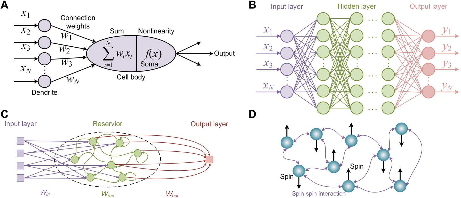
(A) Schematic of a biological neuron. (B) The model of fully connected neural network. (C) Schematic of a standard RC. (D) Schematic of an Ising machine model.
Reservoir computing (RC), derived from the concept of liquid-state machines [67] and echo state networks [68], belongs to a kind of novel computation model of recurrent neural network (RNN). Same as ANN, reservoir computing model consists of three parts, named as input layer, reservoir (hidden layer), and output layer, as shown in Figure 1C. However, the weight matrix between the input layer and the reservoir, and the internal connections of the reservoir are untrained, and only the readout weight denoted by from the reservoir to the output layer is updated in the training process of RC [16, 69]. Here, N is the number of the neurons in the reservoir and M is the input dimensionality of the input information. And K denotes the output dimensionality of the output layer. In the training process of RC, the reservoir state is collected at each discrete time step t, followingwhere fNL is the nonlinear activation function, u(t) is the input signal at the current time step, x(t) and x(t-1) are the reservoir’s internal states at the current time step and the last time step, respectively. The readout y(t) at the current time step is calculated followingwhen performing off-line training for RC, ridge regression is usually used to get the readout weights [69].where is a feature matrix of horizontally concatenated state vectors x(t), is the transposition of . is the target matrix corresponding to the desired optimal computational results, Q denotes the number of training feature vectors, is a small regularization coefficient and I is the identity matrix. As the internal parameters of RC are unmodified in the training process, the training convergence is efficiently achieved compared to general RNN [70]. Moreover, this advantage of RC makes it friendly to hardware implementation, especially the ORC has attracted much attentions [69, 71, 72] due to the parallelism and high speed of photons. Based on the connection mechanism in the reservoir, ORCs can be mainly divided into two categories: spatially distributed ORCs (SD-ORCs) and time-delayed ORCs (TL-ORCs) [16]. The SD-ORCs construct spatially distributed connection topologies of the reservoir layer so that the parallelism of photons can be maximally utilized [50, 73–77]. The TL-ORCs are mainly implemented by using a single nonlinear node subject to a delayed feedback, which reduce the structural complexity of reservoir and reduce the difficulty for realizing the nonlinearity in optics [53, 65, 78, 79].
Ising machine (IM) is a kind of efficient model to solve the combinatorial optimization problems and nondeterministic polynomial time (NP)-hard/NP-complete problems. Solving these problems are important tasks for various application areas, including operations and scheduling, drug discovery, finance, circuit design, sensing, and manufacturing [80, 81]. However, due to the exponential growth of complexity with the problem size, these problems are very difficult to be solved on conventional von Neumann-based computers. Ising model provides an alternative method to efficiently solve these NP-hard or NP-complete problems by mapping them onto ground-state search problems of the Ising model with polynomial resources [82]. As shown in Figure 1D, the illustrated Ising model has nine spins and each spin occupies one spin state, either spin-up (σi = + 1) or spin-down (σi = − 1). The spin-spin interaction is denoted by Ji,j. The Ising Hamiltonian of the Ising model without an external magnetic field is given bywhere N is the total number of spins. When the configuration of spins minimizes the Ising Hamiltonian, the mapped NP problem is solved. Benefiting from the nanophotonic hardware of parallel, low-energy, and high-speed computations [44, 55, 83], the photonic implementation of Ising model (OIM) is one of the most promising candidates to simulate the Ising Hamiltonian. The fundamental of implementing OIMs is to construct optical spin nodes and their interactions. For example, the optical pulse in optical fiber systems [49, 84–86], the spatial mode in free-space systems [87, 88], and the amplitude of coherent light in integrated systems [55, 56] can be used to represent the spin nodes of Ising model. And these systems have demonstrated the advantages of OIMs, such as parallelism, low latency, and nearly free of environment noise.
Coherent integration platform
The silicon photonics, by patterning silicon-on-insulator (SOI) or bulk silicon wafers using lithographic technology, the same silicon substrate can heterogeneously integrate electronic and photonic devices. It provides a wide-bandwidth, high-speed, low-loss, low energy-consumption, and highly compact integration platform for optical signal processing and computing [26, 89, 90]. Due to the low-loss, stable, and anti-interference propagation in silicon waveguides, the silicon integration platform is very suitable to control stable interferences to implement various optical devices, such as modulators [91, 92], logic gates [93], optical switches [94], polarization splitters [95], mode converters [96]. Moreover, benefiting from great advances in silicon-based integration technology, the analog optical computing based on silicon photonic integration has flourished in recent years. Figure 2A summarizes the development history and milestones of the analog optical computing based on the integration platform with coherent photonics. In 1994, Reck et al. proposed an experimental implementation for realizing N × N arbitrary unitary transformations, U(N), in a triangular array of Mach-Zehnder interferometers (MZIs) [97]. Figure 2B shows the schematic of a 2 × 2 reconfigurable MZI, which is the building block for realizing N × N arbitrary unitary transformations. The 2 × 2 reconfigurable MZI consists of two 3-dB (50: 50) directional couplers with one phase shifter (θ) on one of the internal arms of the MZI and another phase shifter (ϕ) at one of the outputs after the second directional coupler of the MZI. The unitary transformation matrix of the MZI, namely UMZI, can be described by the product of the transformation matrices of two 3-dB directional couplers and two phase shifters as the followingwhere B is the transformation matrix of the 3-dB directional coupler. and are the transformation matrices of the phase shifter (ϕ) and the phase shifter (θ), respectively. The MZI can perform arbitrary SU(2) transformation to its inputs, by successively implementing this unitary transformation on two-dimensional subspaces of the full N-dimensional Hilbert space, all off-diagonal elements of the given U(N) unitary matrix will become zero [97]. Thus, the experimental realization of SU(N) unitary matrix can be constructed by sequentially setting up these MZI devices as the sequence of the product of SU(2) transformation matrices. Moreover, by adding a layer of single-mode phase shifters at the inputs, arbitrary unitary matrices can be realized [98]. This research was an important bedrock of the matrix computation approach based on MZI-based networks and inspired many related researches [44, 46, 51, 55, 56, 99–104].
FIGURE 2
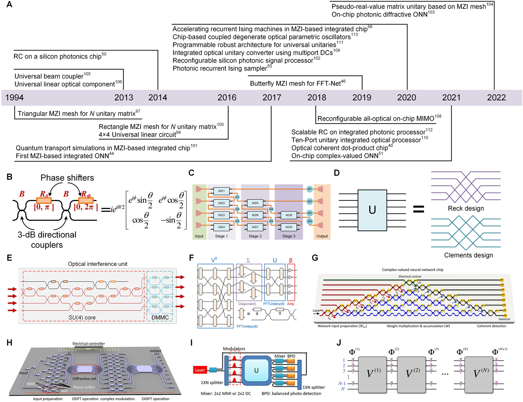
(A) The progresses of analog optical computing in the coherent integration platform. (B) Schematic of a Mach–Zehnder interferometer (MZI). (C) Schematic of a 4 × 4-port universal linear circuit [99]. (D) Schematic of Reck design and Clements design for the unitary implementation [100]. (E) Schematic of the optical interference unit (OIU) [44]. (F) Schematic of the “FFTUnitary” [46]. (G) Schematic of the complex-valued ONN [51]. (H) Schematic of the integrated chip diffractive neural network [103]. (I) Schematic of the pseudo-real-value matrix unitary MZI mesh [104]. (J) A robust architecture for universal unitary [111]. (G) Reprinted from Ref. [51] with permission from Springer Nature: Nature Communications. (H) Reprinted from Ref. [103] with permission from Springer Nature: Nature Communications. (I) Reprinted from Ref. [104] with permission from De Gruyter: Nanophotonics. (J) Reprinted from Ref. [111] with permission from American Physical Society: Physical Review Letters.
In 2013, Miller et al. proposed that MZIs can be organized into a mesh to implement universal beam couplers [105] and universal linear optical components [106]. At the same time, a kind of self-configuration method was proposed to progressively configure these universal beam couplers and linear optical components, requiring no global optimization and continually adjusting itself against changing conditions [106]. It further promoted the application of using the reconfigurable linear optical components for optical computing. Afterwards, based on Miller’s self-configuration method, Ref. [99] demonstrated a silicon implementation of a 4 × 4-port universal linear circuit consisting of a network of thermally tunable symmetric MZIs. The schematic of the integrated circuit is shown in Figure 2C, by the electronic control of phase shifters of MZIs and software feedback, this MZI-based circuit can perform any linear operation between its four input ports and output ports. On the other hand, Clements et al. proposed a brand new architecture of MZIs network for implementing general unitary matrix transformation [100]. The basic idea behind the design was similar to the Reck design [97] that implemented successive SU(2) transformation of MZI components to perform arbitrary U(N) transformation. As shown in Figure 2D, this new design depended on a new mathematical decomposition and achieved the shallower optical depth, requiring roughly half the depth of the triangular design [97], which can effectively minimize optical losses and reduce fabrication resources. Moreover, the rectangular symmetry of this new design greatly improved the robustness to fabrication errors caused by mismatched optical losses. Since then, the analog optical computing (such as ONNs and OIMs) based on MZI-networks has developed rapidly. In 2017, Shen et al. proposed a programmable nanophotonic processor featuring a cascaded array of 56 programmable MZIs in a silicon photonic integrated circuit for a fully ONN [44]. The schematic of the core of the 4-port programmable nanophotonic processor, namely the optical interference unit (OIU) is shown in Figure 2E. The red-part MZIs array performed SU(4) transformation in terms of Reck decomposition principle [97] and performed complete U(N) transformation by cascading the blue-part diagonal matrix multiplication core (DMMC). Based on singular value decomposition, the arbitrary real matrix M can be decomposed into M = U Σ V†. Where U, V† are unitary matrices that can be achieved by OIU, and Σ is a diagonal matrix that can be realized by the DMCC of OIU. By tuning the phase shifters integrated in the OIU, MVM operation of ANN can be passively performed at the speed of light. This ONN architecture demonstrated an enhancement in computational speed and power efficiency over advanced electronics for conventional inference tasks and motivated the attentions on ONN field. In the same year, this type of MZI-based nanophotonic processor was used to simulate the quantum transport [101]. The low-loss and high-fidelity programmable transformations of the integrated processor showed its potential advantages for many-boson quantum simulation tasks. Soon, Fang et al. proposed another better fault tolerance architecture named “FFTUnitary” to implement ONN [46]. As shown in Figure 2F, compared to Reck and Clements design [97, 100], “FFTUnitary” was composed of butterfly-mesh MZIs, which had been demonstrated to realize the discrete Fourier transform (DFT) unitary transformation by Cooley-Tukey FFT algorithm [107]. Despite being non-universal and lacking a decomposition algorithm, “FFTUnitary” can reduce the depth of the unitary multipliers from N to log2(N) so that the robustness of “FFTUnitary” to fabrication errors was improved and the overall noise and loss in the network were reduced. Afterwards, in 2020, the MZI-based silicon photonic integrated circuit was demonstrated as a fully reconfigurable signal processor [102]. A self-configurating method was proposed to program the MZIs without any information about the inner structure. By using this method, the MZI-based integrated circuit can implement various functions, including multichannel optical switching, optical MIMO descrambler, and tunable optical filter. Besides, the above mentioned MZI-based unitary implementation was applied in the photonic recurrent Ising sampler (PRIS) [55, 56], which was a heuristic method tailored for parallel architectures allowing fast and efficient sampling from distributions of arbitrary Ising problems. Because the recurrent photonic transformation of PRIS is a fixed function, the machine was compatible with GHz clock-rate optoelectronic devices that can achieve orders-of-magnitude speedups in solving NP-hard problems.
Afterwards, some researches for improving the ability of information expressivity of the single-layer MZI mesh and reducing the complexity of the MZI-based network have been demonstrated [51, 103, 104]. In 2021, Zhang et al. proposed complex-valued ONN with MZI-based networks [51]. To recover the natural complex-valued operation ability of optical computing, on-chip coherent detection method based on phase-diversity homodyne detection was utilized to determine the relative phase of the output signal to the input signal. As shown in Figure 2G, the red marked MZIs were used for the input preparation, the blue marked MZIs performed the MVM operation, the green marked MZIs separated the reference light that will later be used for coherent detection, and the MZIs marked in grey were used for on-chip coherent detection. The benchmark results showed that the complex-valued calculation can provide stronger learning capabilities, including high accuracy, fast convergence, and the capability to construct nonlinear decision boundaries. In 2022, Zhu et al. [103] demonstrated an integrated diffractive neural network and realized typical computing operations (convolution and matrix multiplication). As shown in Figure 2H, two ultracompact diffractive cells were used to implement optical discrete Fourier transform (ODFT) operation and optical inverse discrete Fourier transform (OIDFT) operation. Between the two diffractive cells, the N-array MZIs were used to achieve the complex-valued modulation. Similar to the principle in Figure 2F, the overall can perform convolution and matrix multiplication through programming phase shifters of MZIs. This implementation resulted in reducing the component number from N2 to N so that a ∼10-fold reduction in both footprint and energy consumption was achieved compared to previous MZI-based ONNs [103]. Besides, Tian et al. proposed another MZI-based implementation that can reduce half of components of unitary multipliers [104]. The previous MZI-based ONN mainly relied on SVD algorithm, the real-value weight matrix of ONN was decomposed into two unitary matrices and one diagonal matrix. Actually, the real part of single unitary matrix had enough freedom to express the real-value weight matrix. The schematic of the pseudo-real-value matrix unitary MZI mesh for matrix expression is shown in Figure 2I, U represented a kind of MZI-based unitary implementation [100], a beam of reference light was split from the input light and then distributed into N output branches, the output light of U interfered with the reference light by the mixer and then was detected by the balanced photodetector to determine the real part of the multiply result. By employing the real-part of a unitary mesh to learn the real-value matrix, the requirement of MZIs was reduced least to O(Nlog2N) level. As the requirement of MVM scale gets larger, low level complexity component design will be more competitive in robustness and power efficiency [46, 103].
On the other hand, due to the natural sensitiveness of MZI-based networks to the manufacturing errors, researcher tried to develop other robust architectures to realize unitary matrix transformation [108–111]. In 2018, Tang et al. proposed a new integrated architecture [108] consisting of phase shifter layers and multimode interference (MMI) coupler layers to perform multi-input-multi-output (MIMO) demultiplexing. This combination of mode mixing component (MMIs and multiport directional couplers [109, 110]) and single-mode phase shifter revealed an alternative method to perform the unitary transformation or linear transformation and demonstrated stronger robustness for expressing the unitary matrix [111]. Besides, Saygin et al. proposed a multichannel-block robust architecture to implement universal unitary transformations [111]. As shown in Figure 2J, the unitary implementation was composed of multiple phase layers Φ(N) and mixing layers V(N) that introduced interaction between the channels to realize multichannel interference. They numerically demonstrated that enough multi-layer Φ(N) and V(N) can always construct the desired unitary matrix whatever the unitary matrix of the mixing layer was. Moreover, compared to that based on the network of two-channel blocks [100], this architecture was more robust to the fabrication errors. In conclusion, these new architectures improved the robustness of the network to the manufacturing errors but lacked mathematical programming algorithms for the rapid reconfiguration.
Except for the MZI-based analog optical computing, the coherent integrated platform with other types of components can also support the implementation of ONNs [40], ORCs [50, 112], and OIMs [113]. In 2014, Vandoorne et al. firstly demonstrated a 16-node parallel reservoir on a silicon photonics chip consisting of feedback loops with a combination of 1 × 2 and 2 × 2 multimode interferometers and delay lines with shallow-etched spiral waveguides [50]. The passive photonic silicon reservoir was used to perform both digital and analogue computational tasks to show its capacity as a generic integrated computational platform for wide applications. Afterwards, in 2020, Okawachi et al. [113] demonstrated an integrated silicon-nitride photonic circuit consisting of spatial-multiplexed degenerate optical parametric oscillators (DOPOs) that can be used to realize a hybrid temporally multiplexed coherent Ising machine to solve NP-hard problems [49, 84, 85]. Then, in 2021, Xu et al. demonstrated a silicon-based optical coherent dot-product chip (OCDC) capable of completing deep learning regression tasks [40]. The weighting operation was finished by the independent modulation of on-chip split coherent light and the summation completed when all branches matched in phase. Meanwhile, the OCDC implemented operations in the complete real-value domain instead of in only the positive domain by introducing the reference light. In the same year, Nakajima et al. demonstrated a scalable on-chip implementation of RC on an integrated coherent linear photonic processor [112]. Compared to previous approaches, the input and recurrent weights of RC were both encoded in the spatiotemporal domain by the integrated circuit consisting of 1: N splitters, delay lines, MZIs, phase shifters, and variable optical attenuators. And the footprint of the input circuit and reservoir circuit were 41 × 46 mm2 and 28 × 47 mm2, respectively.
Incoherent integration platform
In above mentioned coherent analog computing architectures, it is often difficult to independently adjust the elements of the computation matrix as they depend on the overall dependent parameters. For example, the transmission matrix of the MZI-based network is associated with the configuration of all the MZIs [100]. An alternative method is to express the elements of the computation matrix with different wavelengths. Due to avoiding the interference between different wavelengths, the calibration of the computation matrix can be discretely implemented. Thus, the incoherent matrix computation method based on the wavelength division multiplexing (WDM) has been widely applied in analog optical computing [41, 43, 48, 52, 64, 114–118].
Figure 3A summarizes the timeline of advances in analog optical computing based on the incoherent integration platform. In 2012, Fang et al. first experimentally demonstrated MVM operation using a 4 × 4 silicon microring (MRR) modulator array [43]. As shown in Figure 3B, the input vector B was modulated on the optical power of N × 1 LD-array with different wavelengths and the matrix A was represented by the transmissivity of the M × N MRR modulator array. Then, the input vector B was multiplexed and broadcasted into each row of MRR array. In the end, independent modulation of each MRR executed the multiplication and the photodetector performed the accumulation process. As the footprint of MRR was more compact (a diameter of only a few microns) [43] than that of the MZI (over 10,000 μm2) [44, 51] so that it was promising to use the broad spectrum resource (hundreds of channels) [17] to extend the computing density. After that, many MRR-based analog computing architectures have been proposed [41, 64, 114–116].
FIGURE 3
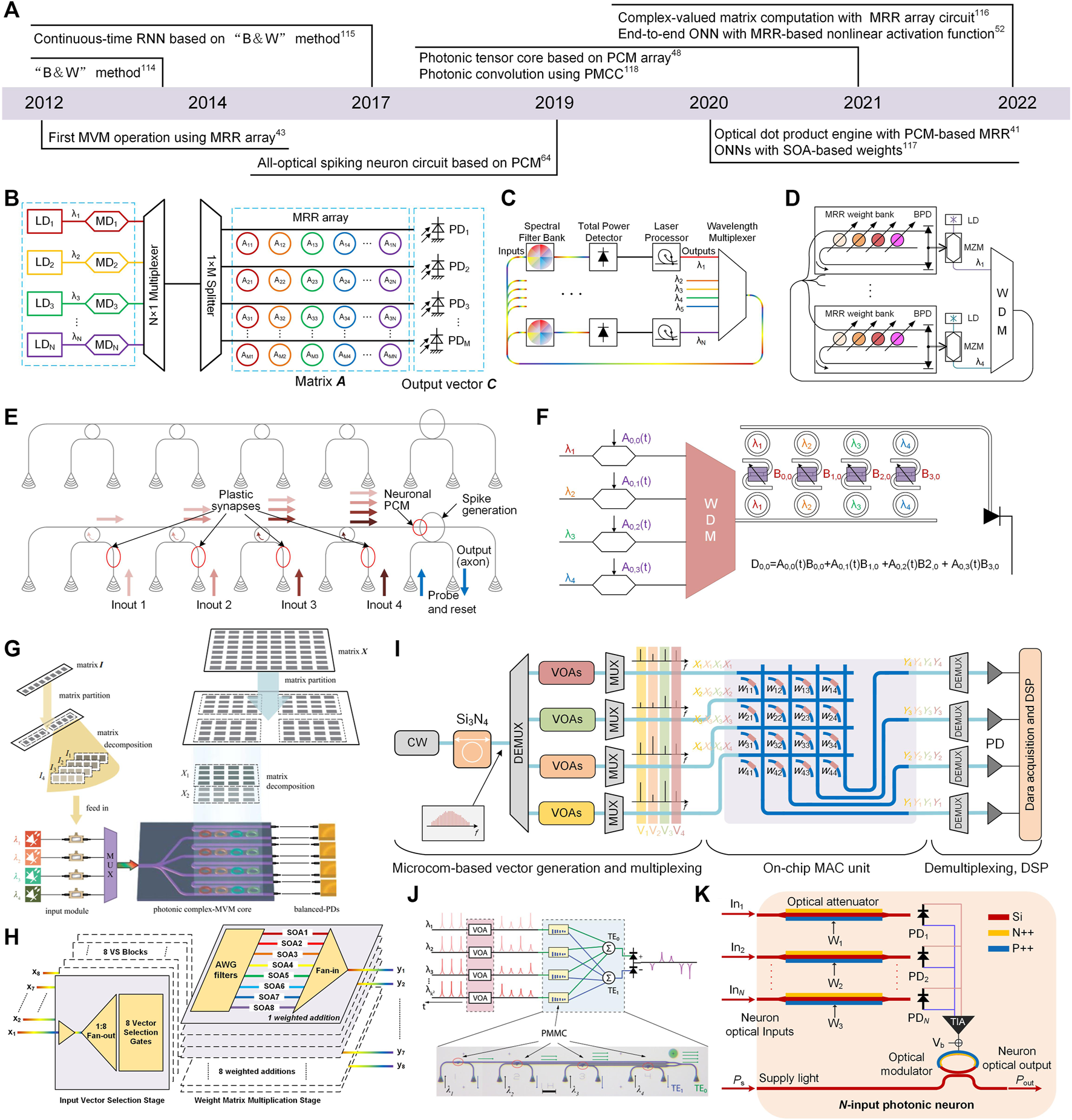
(A) The progresses of analog optical computing in the incoherent integration platform. (B) Schematic of MRR-based optical matrix-vector multiplier [43]. (C) Schematic of an optical B&W network [114]. (D) An experimental setup concept of B&W network [115]. (E) Schematic of the all-optical spiking neural circuit [64]. (F) Schematic of the dot-product engine based on MRR [41]. (G) The principle of MRR-based complex-valued MVM [116]. (H) Schematic of the SOAbased weighted addition operation circuits [117]. (I) Schematic of the photonic tensor core [48]. (J) Schematic of the convolutional photonic computing core using PMCC array [118]. (K) The schematic of an N-input photonic neuron in the integrated end-to-end photonic deep neural network chip [52]. (G) Reprinted from Ref. 116 with permission from Springer: Frontiers of Optoelectronics. (J) Reprinted from Ref. 118 with permission from Springer Nature: Nature Communications.
In 2014, Tait et al. proposed a protocol named “Broadcast and Weight (B&W)” [114] that can be applied in scalable photonic spike processing and optical computing [37, 115]. An optical implementation of B&W protocol on the neural network model is illustrated in Figure 3C. The multiplexed signal collected from each neuron node (laser processor) was equally split and broadcasted into the weight bank (spectral filter bank) of every neuron node. Then, the weight bank operated independent weighting for each wavelength signal belonging to its unique neuron node and the total power detector yielded the sum of the weighted signals. In the end, the neuron node performed the nonlinear activation function of artificial neurons or spiking neurons. This protocol provided a promising way to construct parallel and scalable interconnections between photonic neurons for neuromorphic processing and optical computing. Followed by the protocol, in 2018, Tait et al. demonstrated a recurrent silicon photonic neural network based on the B&W protocol [115]. In this implementation shown in Figure 3D, the weight bank was realized by the MRR array and the photonic neuron was represented by the voltage-driven Mach-Zehnder modulator (MZM). After that, in 2019, Feldmann et al. proposed an all-optical spiking neuron circuit with phase-change material (PCM)-embedded plastic synapses and neurons [64]. As shown in Figure 3E, the previous-layer output spikes were labelled by different wavelengths and weighted through the PCM-embedded waveguide. Then, the weighted signals were multiplexed together by the MRR array. Next, the multiplexed signal was injected into a big ring resonator with PCM embedded at the crossing. In this architecture, the weighting operation was performed by the differential absorption for light under the different phase states (amorphous state or crystalline state) of PCM. And the MRR-based wavelength-division multiplexing technology was used to implement the sum operation. Lastly, the nonlinearity of neurons derived from the PCM-embedded ring resonator. Benefitting from the nonvolatile weights denoted by PCM and all-optical nonlinearity, this type of optical network can process information under ultra-low power consumption. Moreover, combined with the WDM technology, dense integrated MRRs and on-chip optical frequency comb technology [17] provide an ideal platform for large-scale expansion of networks. Similarly, Miscuglio et al. proposed photonic tensor cores by utilizing the dot product engine [41]. The schematic of the dot product engine is shown in Figure 3F. The input vector was loaded on the WDM signals modulated by high-speed modulators (MZMs) and then weighted by the PCM between two cascaded MRRs. The weighted WDM signals were incoherently summed up using a photodetector, which completed the dot product operation. The numerical simulations showed that the photonic tensor core unit had two to three orders higher performance over electrical tensor core units. Afterwards, in 2022, Cheng et al. improved the MRR-based MVM to perform complex-valued matrix computation and demonstrated Walsh-Hardmard transform, discrete cosine transform, discrete Fourier transform, and image convolutional processing in a 4 × 4 MRR array circuit [116]. The working principle of complex-valued MVM is shown in Figure 3G. In order to process full complex MVM, the input matrix I was divided into four matrices, defined as the positive real, positive imaginary, negative real, and negative imaginary parts of the matrix I. The weight matrix X was also divided into the real and imaginary parts and loaded on the MRR array. Moreover, the balanced photodetectors (PDs) were used between the add-drop port and drop port to cover the real number field expressed by the transmission coefficient of MRRs.
Except for using MRRs and B&W to realize matrix calculation, the PCM, SOA, and optical attenuator have been used to implement MVM operations and ONNs [48, 52, 117, 118]. In 2020, Shi et al. proposed another integrated weighting component (semiconductor optical amplifier, SOA) to perform the MVM operation in a WDM network [117]. The schematic diagram for the SOA-based weighted addition operation circuit is shown in Figure 3H. In the input vector selection stage, WDM inputs were fan-out to multiple weight matrix multiplication blocks, followed by an input vector selection unit. Then each arrayed waveguide grating (AWG) of the weighted addition block de-multiplexed the selected WDM inputs and assigned each wavelength channel to an independent SOA to perform the weighting operation, followed by a fan-in unit to addition operation. Compared to MRR-based weight matrix multiplication, SOA avoided the complicated calibration procedure because of the thermal cross-talk between adjacent elements, and monolithic or hybrid integration of gain and non-linear components was very promising to realize the on-chip nonlinearity and all-optical connectivity [119]. Afterwards, in 2021, Feldmann et al. demonstrated a highly parallelized integrated photonic hardware accelerator (tensor core) that operated at speed of 1012 MAC operations per second [48]. The schematic of the tensor core for performing four parallel MVM operations is shown in Figure 3I. The input vectors (V1 to Vn) were modulated by variable optical attenuators (VOAs) on the frequency combs generated by a high-Q Si3N4 photonic-chip-based microresonator and then de-multiplexed into four channels. Combs (X1 to Xn) belonging to the same group of vectors (in the same color as Vn) were parallelly input into the on-chip MAC unit consisting of a 4 × 4 crossing Si3N4 waveguide array and side-coupled PCM array. Four columns of PCMs (weight matrix) synchronously performed the dot product operation with the input vectors (V1 to Vn) so that four complete MVM operations finished at the same time. Then, the four output vectors were demultiplexed and detected in the following procedures. Due to the nonvolatile and zero-energy maintained features of PCM, the tensor core can achieve parallel, fast, and efficient photonic in-memory computing as the optical analogue of an application-specific integrated circuit (ASIC). In the same year, Wu et al. proposed another PCM-based convolution computing scheme by using phase-change metasurface mode converters (PMMCs) to express the matrix element [118]. PMCC was a programmable waveguide mode converter (TE0 to TE1) controlled by the tunable material phase of phase-gradient metasurface (GST). The schematic of a PMMC array for convolution is shown in Figure 3J. A patch of pixels of an image was encoded as optical pulses and input into k2 optical channels. The weight element was mapped into the mode contrast value of PMCC. The output in TE0 and TE1 were summed incoherently and measured by PDs to calculate the convolution result. By measuring the mode contrast, the value of weight can reach a 6-bit resolution, including both positive and negative values, which had an improvement compared to that of measuring the transmission of the optical input data through the programmed PCM [64]. In 2022, Ashtiani et al. demonstrated an integrated end-to-end photonic deep neural network (PDNN) that consisted of the whole functionality of artificial neurons [52]. The schematic of an N-input photonic neuron in PDNN is shown in Figure 3K. The array of P-doped–intrinsic–N-doped (PIN) current-controlled attenuators was used to individually weight the input signal. Then, the outputs of attenuators were converted into photocurrents by PDs and combined as the weighted sum of the neuron inputs. The weighted sum current drove a PN junction MRR modulator to perform the nonlinear activation function. In the on-chip PDNN, the linear operation was performed optically and the nonlinear operation was realized opto-electronically. Moreover, the inference time for the classification task was under 570 ps which was comparable with a single clock cycle of state-of-the-art digital platforms. In conclusion, the incoherently driving analog optical computing mainly depends on the mechanism that different wavelength channels perform independent multiplication and WDM technology performs the fan-out of inputs and the fan-in of outputs. Due to the rich spectrum resources and stability for independently controlling the weights, the WDM-based incoherent integrated circuit is an alternative platform to implement reconfigurable and scalable analog optical computing.
Space-propagation optical platform
Apart from modulating information-carrying light in waveguides to realize analog optical computing, the propagation and interconnection of light in free space can be utilized to achieve high-speed, high-parallelism optical linear operation for analog optical computing. Specially, the density of interconnection can be easily extended to hundreds and thousands. Based on various space optics components, such as the lens, mirror, spatial light modulator (SLM), diffractive-optical element (DOE), digital micro-mirror device (DMD), diffractive layer, most analog optical computing models, including ONNs [47, 63, 120–125], ORCs [74], and OIMs [88], have been widely implemented.
Figure 4A summarizes the timeline of advances in analog optical computing based on the space-propagation optical platform. In 1971, Bieren et al. firstly demonstrated that the Fourier transform operations can be performed without restriction in optical lens system [45]. After few years, a fully parallel, high-speed optical MVM (discrete Fourier transforms) system model was first proposed by Goodman [42]. The principle of optical MVM is depicted in Figure 4B. Firstly, the input vector A was modulated on the intensity of N light-emitting diodes (LED’s) array. Then, the input light beams were collimated by L1 and duplicated in the vertical direction by the cylinder lens (CL1). After passing through the CL1, the duplicated input vectors parallelly performed multiplication operation with each raw vector of the matrix mask B (SLM). Next, the beams from a given raw passed through the lens CL2 and converged (addition operation) on one element of the vertical photodetectors array. By copying the input vector and mapping the duplicates on the matrix mask, the MVM operation was naturally performed in the propagation process. Afterwards, Athale et al. proposed three implementations using outer product decomposition to realize optical matrix-matrix multiplier [126]. These methods mainly utilized the light source, the light modulators (electro-optic modulations, direct driven LED array, and acoustooptic Bragg cells), and the 2-D detector array to construct the product operation. However, the optical Fourier transform was not fully explored to be applied in optical computing in the past. In recent years, due to the activity of analog optical computing, optical Fourier transform has flourished again and promoted its applications in analog optical computing [47, 103, 120–122].
FIGURE 4
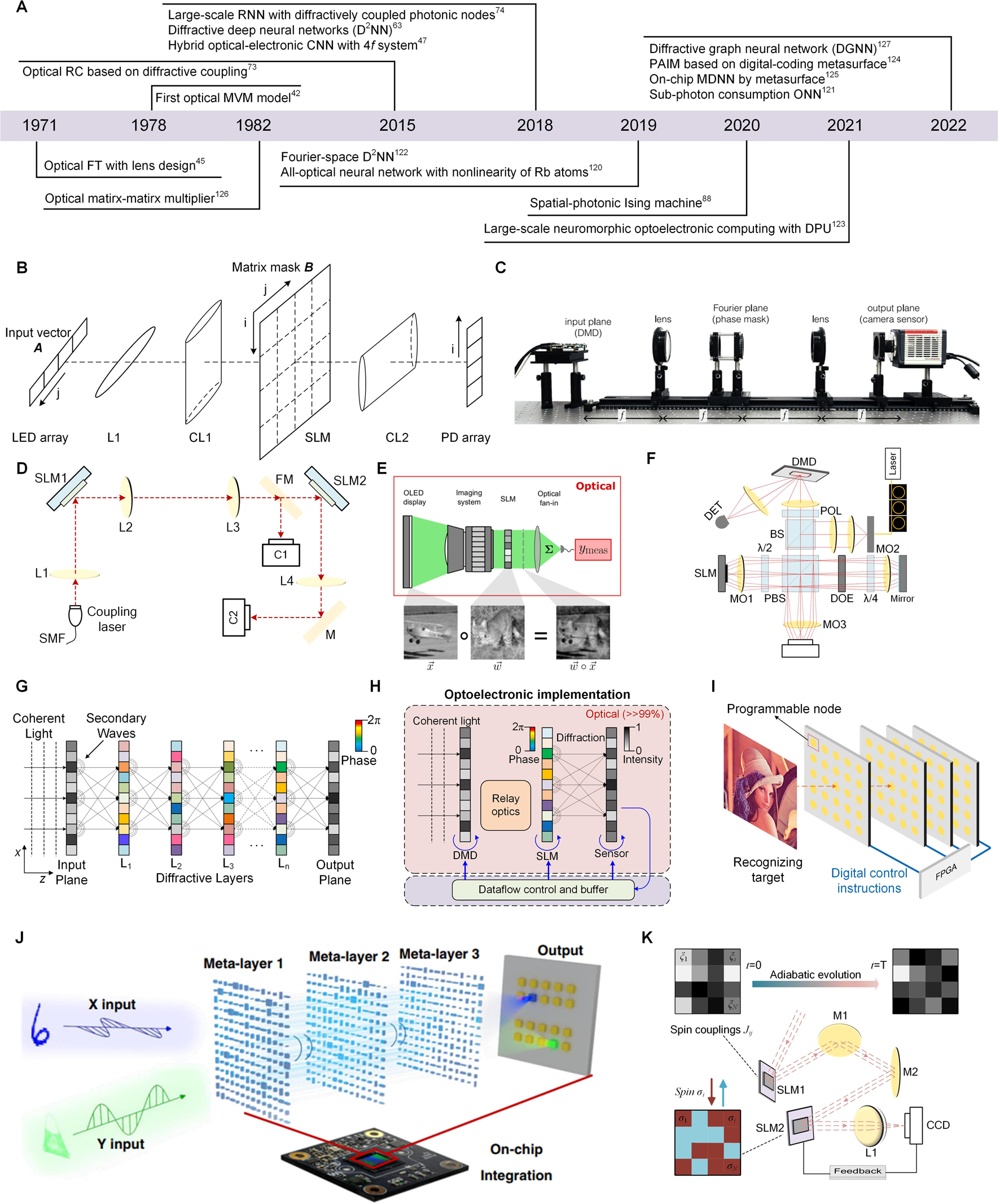
(A) The progresses of analog optical computing in the space-propagation optical platform. (B) Schematic of the optical MVM model. (C) Schematic of the optical convolutional layer based on 4f system [47]. (D) Schematic of the linear operation in the all-optical neural network [120]. (E) The procedure for characterizing optical vectorvector dot products [121]. (F) Schematic of the optical recurrent neural network using SLM and DOE [74]. (G) Schematic of the diffractive deep neural network [63]. (H) Schematic of the reconfigurable diffractive processing unit (DPU) [123]. (I) An array of programmable metasurfaces for constructing the programmable artificial intelligence machine [124]. (J) The working principle of the onchip multiplexed diffractive neural network [125]. (K) Principle of the spatial-photonic Ising machine [88]. (C) Reprinted from Ref. 47 with permission from Springer Nature: Scientific Reports. (E) Reprinted from Ref. 121 with permission from Springer Nature: Nature Communications. (J) Reprinted from Ref. 125 with permission from Springer Nature: Light|Science and Applications.
In 2018, Chang et al. proposed a hybrid optical-electronic convolutional neural networks with 4f system implementing optical convolution [47]. Based on the convolution theorem, the convolution of two-dimensional continuous functions in the space domain can be obtained by the inverse transformation of the product of their corresponding two Fourier transforms. The optical convolutional layer design based on 4f system is depicted in Figure 4C. The input image was encoded on the intensity of coherent light by the DMD and converted into the Fourier space after passing through the first lens. The convolution kernel was mapped into the point spread function (PSF) of the phase mask that placed on the common Fourier plane of two lenses. When the input beam passed through the phase mask and the second lens, the convolution result was naturally imaged on the camera sensor. By tiling the multiple kernels, multiple parallel convolutions were performed simultaneously so that the computational burden in CNN was greatly reduced. After that, in 2019, Zuo et al. proposed an all-optical neural network using SLM and Fourier lenses for linear operation and using laser-cooled 85Rb atoms for nonlinear operation [120]. The schematic of the linear operation is shown in Figure 4D, the input coupling laser beam was collimated and illuminated onto the first SLM (SLM1), which selectively reflected separate beam spots as the input vector Xj. The flip mirror (FM) and the first camera (C1) were used to monitor and measure Xj. Then, the incident light beam Xj was split and modulated by SLM2 into different directions i with weight Wij. In the end, the Fourier lens L4 summed all diffracted beams in the same direction onto a spot at its front focal plane as the linear summation Yi = ∑jWijXj. After the linear operation, the laser-cooled 85Rb atoms in a dark-line two-dimensional magneto-optical trap (MOT) implemented an electromagnetically induced transparency (EIT) nonlinear activation function. Under the motivation of figuring out the clean and quantitative investigation of the limits of optical energy consumption in large-scale ONNs. In 2022, Wang et al. demonstrated a sub-photon consumption ONN using spatial mode to perform the optical dot product [121]. The schematic for implementing sub-photon optical vector-vector dot product is shown in Figure 4E. The elements of the input vector were encoded in the intensity of independent spatial modes illuminated by an organic light-emitting diode (OLED). And the SLM was used to represent the weight by encoding the transmissivity of the modulator pixel. The scalar multiplication was performed when the emitting beam passed through the SLM. Lastly, a lens was used to focus the transmitted light onto a detector, where the total number of photons impinging on the detector was proportional to the dot product result. The result of the sub-photon consumption successfully proved that the energy consumption of ONNs can reach to an extreme low level.
Different from using optical Fourier lens to implement MVM operation, the direct phase/amplitude modulation on the diffractive lights also can implement highly parallel MVM operation. In 2015, Brunner et al. proposed a diffractive-optical network consisted of diffractive orders of a diffractive-optical element (DOE), imaging lens, and vertical-cavity surface-emitting lasers (VCSELs) array, allowing for constructing the parallel ORC [73]. The diffractive optical coupling in this diffractive-optical network was used to achieve the connection of different neuron in the reservoir and the connection weight was implemented by the coupling between individual lasers of the VCSEL. Based on this concept, in 2018, Brunner’s team further proposed a large scale recurrent neural network with 2025 diffractively coupled photonic nodes by using a SLM and DOE [74]. The schematic of the recurrent neural network is shown in Figure 4F. Firstly, the beam of the illumination laser passed through the beam splitter (BS) and focused on the first microscope objective’s (MO1) back focal plane and illuminated the SLM. Then, the pixel of SLM operated the intensity modulation on the illumination field, which represented encoding the RNN state. After that, the transmitted field was imaged on a mirror through MO2, then imaged on the camera after a double-pass through the λ/4-plate and the reflection of the PBS. The DOE adding to the beam path was used to implement the internal connection weight WDOE in RNN. The network’s new state was denoted by the intensity transmitted through the PBS. Lastly, the computational result was read out after summing the network’s state according to weight matrix WDMD, which was loaded on the DMD. After learning the readout weight of WDMD, the 900-node recurrent neural network can implement low-error chaotic Mackey–Glass sequence prediction despite the Boolean readout weights.
In 2018, an important novel spatial optical computing architecture named “diffractive deep neural network (D2NN)” was proposed by Lin et al. [63]. This research opened up the study direction of using the successive modulation of diffractive plane layers to implement MVM operation and ONNs. As shown in Figure 4G, the D2NN was consisted of multiple diffractive layers, whose every pixel acted as a neuron of artificial neural network, with a complex-valued transmission (or reflection) coefficient. According to the Huygens-Fresnel’ equation, the diffraction of wave between the successive layers can represent the fully connection of neurons. These transmission/reflection coefficients of each layer would be fixed and the diffractive layers would be physically fabricated after training the whole network by simulation, then the D2NN can passively perform the computing function in the speed of light. Due to the dense connections (millions of neurons and billions of connections), the phase-only modulated D2NN can realize 91.75% and 81.1% classification accuracy for MNIST and Fashion-MNIST, respectively, without implementing nonlinear activation function. Next year, Yan et al. demonstrated that the D2NN placed in the Fourier space can obtain better performance in advanced computer vision tasks, including all-optical saliency detection and high-accuracy object classification [122]. Compared to the real-space D2NN, the Fourier-space D2NN was more natural to preserve the spatial correspondence by incorporating a dual 2f optical system, which was helpful for those tasks that required an image-to-image mapping. Moreover, a photorefractive crystal (SBN:60) was used after D2NN to further improve the ability of the network to extract features. After training, the Fourier-space D2NN realized 98.6% and 91.1% classification accuracy for the MNIST and Fashion-MNIST dataset, respectively. In conclusion, the D2NN framework provided a unique all-optical processing platform that efficiently operated at the speed of light using passive components and optical diffraction. Meanwhile, the scale of D2NNs can be easily extended to provide extreme parallelism by using high-throughput and large-area 3D fabrication methods or on-chip integration. After that, in 2021, Zhou et al. [123] proposed using the reconfigurable diffractive processing unit to implement large-scale neuromorphic optoelectronic computing. The basic computing unit for constructing different types of ANN architectures was a reconfigurable diffractive processing unit (DPU) whose schematic is depicted in Figure 4H. Here, the design was used to process large-scale visual signals that feed in images and videos. Thus, the DMD and SLM were used as the modulators to implement the input nodes due to its high data throughput. Different input nodes were physically connected to individual output neurons by the diffraction, where the connection weights were determined by the diffractive modulation of the wavefront. The COMS sensor was used to as the photodetector to implement the optoelectronic neurons. By temporally multiplexing these DPUs, three complex ANN architectures were demonstrated, including the diffractive deep neural network (D2NN), diffractive network in network (D-NIN-1), and diffractive recurrent neural network (D-RNN). Soon after, Yan et al. proposed to realize all-optical graph representation learning by using integrated diffractive photonic computing units (DPUs) [127]. The DPU was consisted of the successive diffractive layers to transform the node attributes of graph network into optical neural messages. The proposed diffractive graph neural network (DGNN) opened up a new direction for designing application-specific integrated photonic circuits for high-efficiency processing large-scale graph data structures.
On the other hand, improving the reconfigurability and integration of D2NN became another promising research direction nowadays. In 2022, Liu et al. proposed a new kind of diffractive deep neural network by using multi-layer digital-coding metasurface array, which was named as the programmable artificial intelligence machine (PAIM) [124]. As shown in Figure 4I, the pre-designed diffractive layers in Ref. [63] were replaced by digital-coding metasurfaces consisting of multiple programmable nodes. By using field-programmable gate arrays (FPGAs) to control these nodes, the metasurfaces can manipulate reflected or transmitted electromagnetic waves in real time. Compared to previous diffractive deep neural network, the PAIM was fully reprogrammable and re-trainable owing to its weight-reprogrammable nodes, which facilitated the flexible configuration in different applications. In the same year, Luo et al. proposed on-chip multiplexed diffractive neural network (MDNN) by metasurface [125]. The schematic of the MDNN for polarization-dependent object classification task is depicted in Figure 4J. The input light was encoded with different information of a handwritten digit and a fashion product in x-polarization and y-polarization, respectively. By tuning the structural parameters of each meta-unit, the metasurface can implement polarization-dependent phase responses in x-polarization and y-polarization. Then, the final diffractive results of different polarizations converged on the corresponding photoelectric detection region on the CMOS chip. The polarization multiplexing scheme opened up a novel way to implement massively parallel computing tasks.
Besides, the space-propagation optical platform can be used to implement OIMs. In 2020, Pierangeli et al. proposed a spatial-photonic Ising machine by using SLM and demonstrated the adiabatic evolution of frustrated Ising models [88]. The experimental setup of the spatial-photonic Ising machine is shown in Figure 4K. The SLM2 encoded Ising spins σi = ±1 on a continuous beam by 0-π phase-delay values. The SLM1 was used to implement the intensity modulation on ξi to control spin interaction. The CDD was used to measure the difference between the pre-determined target image and the image detected. Based on the feedback of CDD, the system was firstly optimized to reach the minimum of a Hamiltonian with homogeneous couplings, then the adiabatic evolution was simulated. This spatial-photonic Ising machine based on SLM provided an alternative method to support large-scale systems consisting of millions of spins.
Optical fiber platform
As above mentioned, many integrated optoelectronic devices have been demonstrated in recent decades, including optical filters [128], optical couplers [129], logic gates [130], modulators [91, 131], polarization splitters [95], mode converters [96], photodetectors [132] and so on, and they have been applied in analog optical computing systems [44, 64, 103, 115]. However, the monolithic integration or heterogeneous integration of passive and active devices is still challenging [133, 134]. Meanwhile, the technological path and architecture design for analog optical computing just have started to flourish and still been developed. Thus, innovative ideas are still being encouraged compared to mature prototypes for commercial products. Due to the flexibility for restructuring with the optoelectronic devices and measuring instruments in the optical fiber communication field, many computation prototypes based on the optical fiber platform also have been proposed for realizing high-performance analog optical computing [18, 49, 53, 54, 65, 78, 79, 84, 85, 135].
The development history of the analog optical computing based on the optical fiber platform is summarized in Figure 5A. These researches mainly focus on the implementation of ORCs and OIMs, and fewer are related to ONNs. In 2012, three associated researches of optoelectronic and all-optical RCs by using a single nonlinear node subject to a delayed feedback were successively proposed [53, 65, 78]. At first, Paquot et al. demonstrated an optoelectronic implementation of RC [53] based on a previous proposed similar architecture [136] that consisted of a single nonlinear node and a delay line. The experimental setup of the optoelectronic RC is shown in Figure 5B. The core of this RC implementation was the closed loop consisting of Lithium Niobate Mach-Zehnder modulator (M-Z) and a fiber spool, which performed as a nonlinear node to provide a sine nonlinearity and acted as a memory to store the delayed states of the nonlinearity, respectively. Besides, the input signal was fed into the system using arbitrary waveform generator (AWG), the response of the system was recorded through the readout photodiode, and the feedback signal was converted from optical field to electronic field by the feedback photodiode and was rejected into the system combined with input signal after being scaled by optical attenuator. By using computer to optimize the readout weight, the performance of the optoelectronic RC in nonlinear channel equalization and speech recognition tasks was comparable to state-of-the-art digital implementations. Soon, Larger et al. demonstrated a similar experimental scheme for optical information processing using a nonlinear optoelectronic oscillator subject to the delayed feedback [78]. The schematic of the optoelectronic implementation of RC is shown in Figure 5C. It can be seen the major component of the setup was similar to that of Ref. [53] but the nonlinearity derived from the Mach-Zehnder modulator turned into a sin2-function. After employing spoken digit recognition and time series prediction tasks as benchmarks, the optoelectronic RC also achieved competitive performance, which proved that the particular type of the nonlinearity seemed not to be crucial for RC. After that, Duport et al. improved the optoelectronic RC [78] and demonstrated the first all-optical experimental implementation [65]. The experimental set-up of the all-optical RC is shown in Figure 5D. The all-optical nonlinear feedback loop was consisted of an isolator, a SOA, a variable optical attenuator, and a fiber spool that acted as delay line. Different from the design of Ref. [78], the nonlinearity was provided by the saturation of the optical gain in SOA, where the characteristics of nonlinearity can be adjusted by controlling the injection currents of the SOA. The utilization of all-optical nonlinearity avoided the loss of velocity suffered from the conversion from optical field to electronic field. Thus, this implementation constituted a significant step towards the possible development of analog optical computing.
FIGURE 5
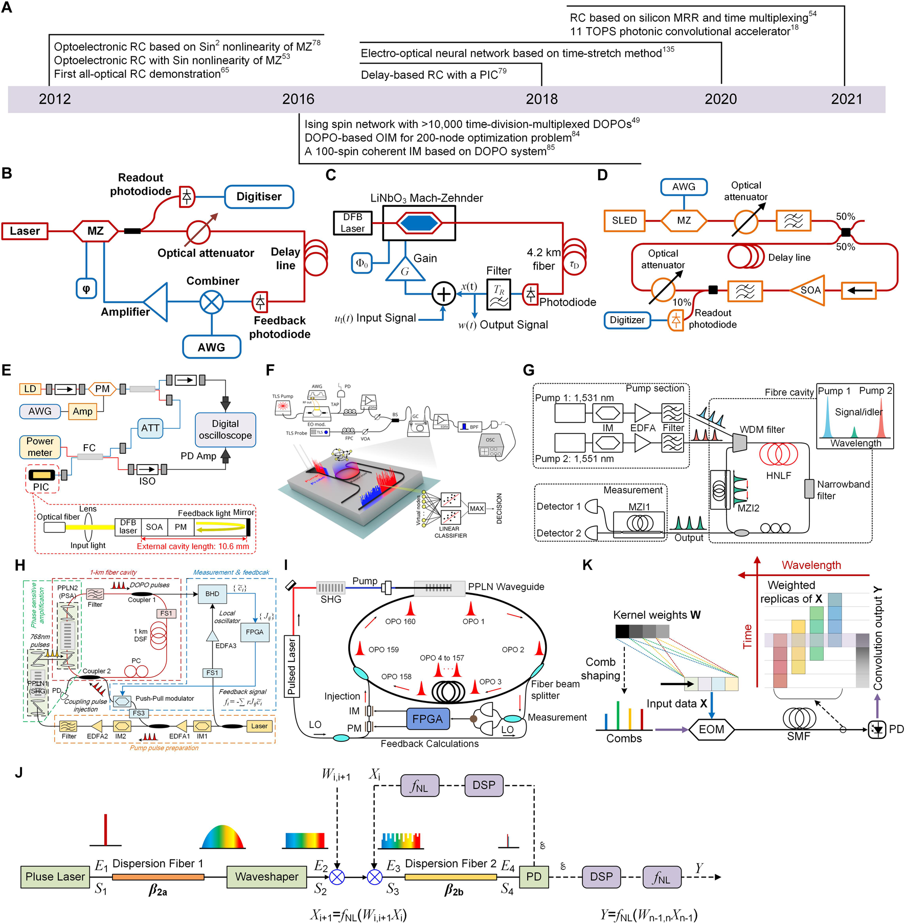
(A) The progresses of analog optical computing in the optical fiber platform. (B) Experimental set-up of the optoelectronic RC based on a single non-linear node and a delay line [53]. (C) Schematic of the optoelectronic implementation of RC [78]. (D) Schematic of the alloptical RC using the SOA as non-linearity [65]. (E) Schematic of the setup for delay-based RC using a photonic integrated circuit as nonlinearity [79]. (F) The experimental setup of the MRR-based RC [54]. (G) The principle of generating artificial Ising spins based on DOPOs [49]. (H) Schematic of the setup of the coherent Ising machine with measurement and feedback [84]. (I) Schematic of the coherent Ising machine by using PPLN to form the timedivision-multiplexed pulsed DOPOs [85]. (J) The principle of the time-stretch electro-optical neural network [135]. (K) The working principle of the photonic convolutional accelerator [18]. (F) Reprinted from Ref. 54 with permission from Springer Nature: Scientific Reports.
Afterwards, some researchers aimed to the integration of ORC and demonstrated some methods. In 2018, Takano et al. proposed a compact delay-based RC [79] by using a photonic integrated circuit (PIC). Here, the nonlinearity of RC was implemented by the nonlinear dynamics in the PIC with short external cavities. The structure of the RC and PIC is demonstrated in Figure 5E. The reservoir was implemented through the PIC with time-delayed optical feedback, and the input signal was injected into the reservoir using a semiconductor laser diode (LD) and a phase modulator (PM). The output signal was sampled from the temporal waveforms of the PIC using a photodetector and digital oscilloscope. As shown in Figure 5E (bottom), the PIC was consisted of a distributed-feedback (DFB) semiconductor laser, a SOA, a PM, a passive waveguide, and an external mirror for optical feedback. By the optical fiber connected to the PIC through a lens, the output of the PIC can be detected and input signal can be injected into the PIC. As the delay time of the PIC-based feedback loop was very small, two method were proposed to increase the number of virtual nodes of RC, namely reducing of the node interval and using of multiple delay times. After training, this RC with the PIC demonstrated successful performance in time-series prediction and nonlinear channel equalization tasks. After that, Borghi et al. demonstrated an implementation of RC based on a silicon MRR and time multiplexing [54]. The schematic of the experimental setup is depicted in Figure 5F. The input signal was encoded in the intensity of a pump laser and resonantly coupled to the input port of an MRR. Then, the input information was nonlinearly transferred from the pump light to a continuous wave probe laser by generating carriers through two photo absorption (TPA) and free carrier dispersion in the MRR. In this implementation, there was no external feedback and the virtual nodes were realized by time-multiplexing method. Besides, the nonlinearity was naturally provided by the TPA and carrier dynamics served as the connections between the virtual nodes. After computing, the probe light carried the results and exited from the drop port of the MRR. The reservoir achieved a minimum detectable bit error rate (BER) of 1.4 × 10⁻³ for bitrates up to 30 MHz in 1-bit delayed XOR task and 99.3% accuracy in the classification of the Iris dataset. In conclusion, the proposed method of using a single nonlinear node subject to delayed feedback for implementing RCs [53, 54, 65, 78, 79, 136, 137] was an inspiring attempt to reduce the complexity of the reservoir and the difficulty for realizing the nonlinearity in optics. However, the method creates many virtual nodes by using time dimension to exchange space dimension so that the bandwidth of components is challenging compared to that of RCs with parallel nodes.
On the other hand, OIMs based on the degenerate optical parametric oscillator (DOPO) attracted much attention and many researches have been reported [49, 84, 85]. In 2016, three important related works were successively reported. Inagaki et al. demonstrated >10,000 time-division-multiplexed DOPOs and simulated a one-dimensional Ising model [49]. The experiential setup by using DOPOs to generate Ising spins is shown in Figure 5G. As mentioned in Eq. 4, the elements with a binary degree of freedom is required to model the spins of Ising machine and the coupling between spins can be programmable in some way. In this implementation, the stable artificial spin was realized by a DOPO that took only the 0 or π phase relative to the pump phase. To obtain larger number of spins, dual-pump four-wave mixing (FWM) in a highly nonlinear fibre (HNLF) placed in a fibre cavity was utilized. As the number of independent DOPO was proportional to the cavity roundtrip time, increasing the pump repetition frequency or by increasing the cavity roundtrip time can get larger number of spins. Moreover, the spin–spin interaction can be simply implemented with mutual injections of DOPO lights using delay interferometers. Then, Inagaki et al. improved the coherent Ising machine (CIM) [49] and increased the number of spins to 2048 with full spin-spin couplings [84]. And the measurement and feedback (MFB) scheme was used to implement all possible connections among 2048 spins, which provided the foundation to solve 200-node maximum cut problems on arbitrary graph topologies. The schematic of the CIM with MFB is shown in Figure 5H. The periodically poled lithium niobate (PPLN) waveguide placed in a 1-km fiber cavity was used as a phase-sensitive amplifier (PSA) to generate DOPO pulses. The coupler one extracted the DOPO pulses into the balanced homodyne detection (BPD) to measure the phase components {} of the signal DOPOs for every circulation of the DOPOs. The specified spin-spin connection matrix {} and measured {} were input the FPGA to calculate the feedback signal for every DOPO circulation. Then, the feedback signal was modulated on the coupling pulses by the push-pull modulator and reinjected into the cavity through the coupler 2. For the 200-node maximum cut problems with complete graph, the CIM outperformed simulated annealing in terms of accuracy and computation time. At the same time, McMahon et al. presented a 100-spin CIM [85] based on the DOPOs system and MFB scheme as shown in Figure 5I. Dirven by the same principle of CIM, the experimental setup was basically consistent with that of Ref. [84]. Thus, the research focused on discussing the solving of different Ising problems (undirected and unweighted graphs) and the relation between the performance of CIM and the problem size. The results revealed that the total computation time required to obtain ground states (100% accuracy) grows rapidly with problem size N. However, the growth in total computation time was far less severe when the required solution accuracy was reduced. In conclusion, the coupled DOPOs system was demonstrated as an alternative and promising physical system to solve the large-scale Ising problem with scalability and full programmability.
Besides, the optical fiber platform has inspired some novel ideas to implement efficient MVM operations for ONNs. In 2020, Zang et al. proposed an electro-optical neural network using time-stretch method [135]. The time-stretch method was applied to optically perform the linear operation (MVM) in the electro-optical neural network and the nonlinear operation was implemented after converting into the electronic signal. The principle of the time-stretch method is depicted in Figure 5J. Firstly, the ultrashort periodic pulses generated by a mode-locked laser was broadened by the dispersion fiber 1. Then, the broadened pulses were reshaped to flatten by the waveshaper. Afterwards, the flattened broadened pulses were modulated with each row of elements from weight matrix and the input vector in succession. After the modulated pulses passed through the dispersion fiber two and PD, energy of each pulse that implied the result of multiplication of each row of elements from the weight matrix and the input vector was accumulated and then processed with the DSP. By circularly using the setup to implement MVMs and performing nonlinear activations by post-processing, a three-layer electro-optical neural network was constructed and tested in the handwriting digit recognition task with 88% accuracy under considerable noise. In 2021, Xu et al. demonstrated a photonic convolutional accelerator (CA) [18] operating at more than 10 TOPS (trillions of operations per second) by using the dispersion of optical fiber and time multiplexing. The operation principle of the CA is shown in Figure 5K. As first, the input vector X to be processed was modulated by the electro-optical Mach–Zehnder modulator (EOM) on the optical power of multiple frequency combs, whose initial powers were independently reshaped according to the elements of the convolution kernel W. Then, these modulated sequence replicas were delayed at regular intervals after passing through the standard single mode fibre. Ingeniously, the delayed interval caused by the dispersion was set as same with the symbol period of the modulation. Thus, each time slot yielded a convolution between X and W for a given convolution window when the delayed and weighted replicas were summed via high-speed photodetection. Except for the convolution, the CA can realize MVM operations by multichannel wavelength division multiplexing. This architecture sufficiently utilized the advantages of the high-speed modulation of EOMs by simultaneously multiplexing the wavelength dimension and time dimension. Based on the CA, an optical CNN was constructed and showed an accuracy of 88% of the handwritten digit MNIST dataset. In conclusion, although the computing systems based on the optical fiber platform are bulky, these prototypes play an important role in the fast validation of innovative ideas, which is essential for the develop of the analog optical computing.
Nonlinearity and training algorithm
In the previous section, the principle of typical applications (ONNs, ORCs, and OIMs) of analog optical computing was briefly explained and their implementations were discussed when introducing the development history and milestones of analog optical computing by four platforms. In general, the computation of analog optical computing includes two-part operations, namely the linear operation and nonlinear operation. As previous section mentioned, the linear operation can be realized by the coherent interference [44, 51, 103], incoherent summation in WDM system [43, 48, 64, 115], 4f system [47], diffraction [63, 123, 125] and so on. However, the implementation of the nonlinear operation, particularly for ONNs, is not emphatically discussed. In fact, the nonlinearity is crucial for enhancing the computing power of ONNs and accelerating the convergence speed of the network. For example, multiple hidden layers in ONNs are equivalent to a single linear layer without nonlinear activation function so that ONNs cannot learn the nonlinear models and problems. Besides, the nonlinearity in ORCs enables the ability to process sequence problems and complex classification tasks. In recent years, the attention on studying the optical nonlinearity activation functions is focused and many computing architectures with all-optical nonlinearity have been demonstrated [64–66, 120, 122, 138, 139]. On the other hand, the training is a crucial and indispensable step for ONNs and ORCs. By applying the training process to adjust the internal connections and parameters of the network, the network shows the adaptation for different computation tasks. In this section, the implementations of optical nonlinearity in analog optical computing are summarized. Then, the training algorithms used in analog optical computing, particularly in ONNs, are discussed.
Nonlinearity in analog optical computing
In analog optical computing, the implementation methods of nonlinear activation functions can be into two categories, namely optical-electrical-optical (OEO) method and all-optical method. Due to the flexibility and simple implementing, the OEO method was widely applied [37, 140–144]. However, the requirement for the computing speed and power consumption has promoted all-optical nonlinear activation functions in recent years [66, 139, 145–150]. Here, we summarized the implementations of the OEO and all-optical nonlinear activation functions in recent years, and the characteristics of each implementation are depicted in Table 1, including the physical mechanism, the type of nonlinearity function, power consumption/activation threshold, reconfigurability, and integratability.
TABLE 1
| Implementation | OEO/All-optical | Mechanism | Nonlinearity function | Power consumption/Activation threshold | Reconfigurability | Integratability | References |
|---|---|---|---|---|---|---|---|
| PD | OEO | Photoelectric effect | Quadratic function | nW–mW | NO | Compatible | [63, 74] |
| MZM | OEO | Electro-optic modulation | Sin -function; Sin2- function | Vπ: ∼V | NO | Compatible | [53, 78] |
| MRM | OEO | Electro-optic modulation | ReLU; Sigmoid; Radial basis function; Quadratic function | PN junction voltage: 0–1 V | YES | Good | [52, 142, 151] |
| Vπ: ∼2 V | |||||||
| EAM | OEO | Electro-optical absorption | Mirrored sigmoid-like function | Bias voltage: −4 to 4 V | NO | Good | [140, 141] |
| MZI | OEO | Electro-optic modulation | ReLU-like function; Clipped function | ∼10 mW | YES | Excellent | [143, 144] |
| Laser | BOTH | Excitable Behavior; Fano resonance | Excitability dynamics | Pulse energy: | NO | Compatible | [37, 152, 153] |
| 1 pJ–200 nJ | |||||||
| Photonic crystals | All-optical | Optical bistability | Bistable switch | ∼133 mW | NO | Good | [154] |
| SOA | All-optical | Nonlinear gain | Convex function; Sigmoid-like | ∼ mW | NO | Compatible | [65, 146, 148] |
| SESAM | All-optical | Saturation of absorption | Sigmoid-like function | 50 μW–10 mW | NO | Good | [138] |
| MRR | All-optical | Two photon absorption; Kerr effect | \ | 0.5–11 mW | NO | Excellent | [66, 155] |
| Atoms | All-optical | Reverse saturated absorption; Light-induced quantum interference effect; Saturation of absorption | Mirrored sigmoid-like; Electromagnetically induced transparency; ReLU-like | 10−2–102 μJ/cm2 | NO | Poor | [120, 145, 150] |
| 600 µW | |||||||
| 16 μW/mm2 | |||||||
| Nanoparticle | All-optical | Induced transparency | Mirrored sigmoid-like | 102–107 W/cm2 | NO | Compatible | [145] |
| Photorefractive crystal | All-optical | Photorefractive effect | \ | 0.1 mW/mm2 | NO | Poor | [122] |
| Phase change Materials | All-optical | Nonlinear absorption | ReLU-like; Sigmoid-like | Pulse energy: | NO | Excellent | [64, 139] |
| 90 pJ–430 pJ | |||||||
| MZI + MRR | All-optical | Free-carrier dispersion (FCD) effect | Sigmoid-like; ReLU-like; Radial-basis; Softplus | ∼25 mW/π | YES | Excellent | [147, 149] |
The performance and characteristic for different optical nonlinearities.
For the OEO nonlinear activation functions, photodetector (PD) is a common device to realize a quadratic nonlinear function with I = |E|2 (I: intensity of light; E: electric field intensity) when encoding the information on the electric field intensity [63, 74]. Besides, the nonlinear transfer function of electro-optic modulations is widely applied in ONNs and ORCs [52, 53, 78, 140–142, 151]. For example, the transfer function (sin-function and sin2-function) of MZMs was used to implement the nonlinearity of RCs [53, 78]. As the requirement for the type of nonlinearity is not specific, the unchangeable but stable transfer function of MZMs is suitable to consider as the nonlinearity of RC. At the same time, MZMs can provide GHz of bandwidth to implement highly parallel computation. However, the power consumption of maintaining the bias voltage of modulators and loading the modulation signal is relatively higher. Besides, other modulators such as electro-absorption modulators (EAMs) and silicon microring modulators (MRMs) have been used to implement nonlinear activation functions in ONNs [52, 140–142, 151]. In Ref. [140], Amin et al. demonstrated an EAM based on an indium tin oxide (ITO) layer monolithically integrated into silicon photonic waveguides, and its dynamic range was used as the nonlinear activation function in ONNs. The weighted optical signal was converted into photovoltage through a balanced photodiode and then drove the EAM to nonlinearly modulate the laser power mimicking an activation function. Moreover, the ONN based on the nonlinear activation function of the ITO modulator achieved an accuracy of 97% in handwritten classification prediction tasks. In Ref. [142], Tait et al. proposed a silicon photonic modulator neuron consisting of two PDs connected electrically to an MRM. By setting different biasing conditions, the modulator neuron showed six response shapes, including sigmoid shapes widely used in RNNs, ReLU shapes used in feedforward-machine-learning networks, i.e., in multilayer perceptrons (MLPs) and convolutional neural networks (CNNs), radial basis functions (RBFs) applied in machine learning based on support-vector machines, and quadratic transfer functions. This nonlinear configurability demonstrated the potential of the modulator neuron to be applied in a wide variety of neural-processing tasks. In Ref. [52], the MRM was used to implement the ReLU activation function in an on-chip photonic deep neural network, and facilitated 93.8% and 89.8% accuracies in two-class and four-class classification of handwritten letters, respectively. Meanwhile, Williamson et al. proposed an OEO scheme for realizing reprogrammable nonlinear activation functions for ONNs [143]. In this implementation, a silicon MZI was used to modulate the weighted signal by splitting part of the weighted signal and then converting to electrical field to control the modulation phase of the MZI. By adjusting the electrical transfer function, the ReLU-like response and clipped response can be obtained via the interference of MZI. Besides, laser systems can be used to implement the OEO and all-optical nonlinearity via the nonlinear dynamics. In Refs. [37, 152, 153], the excitable dynamics (threshold characteristics) were demonstrated in graphene-based lasers, distributed feedback lasers, and Fano lasers, respectively, which can be applied in optical neuromorphic computing.
Attracted by the energy efficiency and lossless processing speed, all-optical nonlinear activations have begun to appear in recent years with the development of optics and materials science. In early stage, the optical bistability, as a common optical nonlinearity, was proposed to realize the nonlinear activation function [154]. However, the requirement of the operation power was high. In 2012, Duport et al. used the nonlinearity of SOAs to construct all-optical RCs [65]. After that, Alexandris et al. demonstrated an all-optical neuron with sigmoid activation function based on the SOA [146]. The sigmoid function was derived from a deeply saturated differentially-biased SOA-MZI followed by an SOA that performed as a cross-gain modulation-wavelength converter. Then, this SOA-based neuron was used to implement non-gated and gated RNNs and got scores of 41.68% and 41.85% in FI-2010 financial dataset, respectively [148]. However, the integration of SOAs and the power requirement is challenging. In 2014, Dejonckheere et al. proposed the first passive all-optical RC based on a semiconductor saturable absorber mirror (SESAM) [138]. Different from the nonlinearity of SOAs, that of SESAMs performed nonlinear for low values of its input power and performed linear at higher input power. Moreover, SESAMs were passive elements without extra energy to maintain the nonlinearity. Due to the strong nonlinearity in MRRs, the TPA and Kerr effect of MRRs have been used to implement integrated RCs [66, 155]. In 2015, Mesaritakis et al. proposed and modeled an all-optical reservoir computing scheme consisting of randomly interconnected InGaAsP MRRs [155]. Different from the SOA, the computation efficiency benefited from the ultra-fast Kerr effect and TPA of MRRs. Afterwards, in 2018, Miscuglio et al. proposed two independent approaches for implementing nonlinear activation function of ONNs based on nanophotonic structures [145]. The system consisting of a single quantum dot (DQ) between a pair of gold nanoparticles (MNP) demonstrated a classical analogue of plasmon-exciton coupling induced transparency. And the extinction ratios were 1.5 dB and 2.9 dB for single MNP/DQ system and array of MNP/DQs, respectively. Besides, the high-concentration C60 in a polyvinyl alcohol host thin film provided a mirrored sigmoid-like nonlinear function via the reverse saturable absorption with extinction ratio of 6.6 dB. Then in 2019, Zuo et al. demonstrated an all-optical neural network with the electromagnetically induced transparency (EIT) nonlinear function in laser-cooled 85Rb atoms [120]. The EIT effect of the resonant probe beam appeared via the quantum interference between the transition paths in the presence of the coupling beam. After that, Ryou et al. introduced the nonlinear function to the diffraction-based ONNs with the saturable absorption of thermal 85Rb atoms [150]. By the simulation and experiment, their proposed ONNs with a single layer obtained 6% improvement of classification accuracy in image classification of handwritten digits after adding the optical nonlinearity. In 2019, Yan et al. introduced the nonlinearity of the photorefractive crystal (SBN:60) to diffractive deep neural networks for improving the performance [122]. The required incident light intensity for the SBN crystal to excite the nonlinearity effect was about 0.1 mW/mm2, which showed stronger nonlinearity than other optical nonlinear effects, such as the Kerr effect. However, the implementations of nonlinearity with the atom systems and photorefractive crystals are bulky and difficult for integration. In 2019, Feldmann et al. demonstrated an all-optical integrated ONN with the spiking neuron enabled by the nonlinearity of the PCM [64]. By embedding the PCM cell in a silicon ring resonator, the optical resonance condition of the ring was controlled by the phase state of PCMs and a ReLU-like nonlinear activation function was obtained with a contrast ratio of 9 dB. Afterwards, Teo et al. demonstrated a passive all-chalcogenide ONN scheme consisting of Sb2S3-programmed MZI weights and the nonlinear response of Ge2Sb2Te5 [139]. The nonlinear component was consisted of an MRR sedimentated with a piece of Ge2Sb2Te5 thin film that performed a sigmoid-like activation function with a contrast ratio of 9.7 dB. Moreover, a three-layer ONN model with this nonlinearity obtained a maximum training accuracy of 94.5% in MNIST dataset. Due to its nonvolatility and integratability, PCM is a promising platform to realize the low-power-consumption and high-speed optical nonlinearity for analog optical computing. Besides, Jha et al. demonstrated a kind of reconfigurable integrated all-optical nonlinearity by using the MRR-coupled MZI and Mach–Zehnder coupler (MZC) [147, 149]. The nonlinearity was mainly enabled by the free-carrier dispersion (FCD) effect in silicon MRRs, which reacts as a nonlinear phase response to optical power. By pairing with the tuning biases on the MZI, the shape and threshold of the nonlinear activation functions can be programmed. Finally, four types of activation functions, namely sigmoid, clamped ReLU, radial-basis, and softplus were experimentally demonstrated and showed consistency with the theoretical results. And the benchmark simulation obtained accuracies of 100% and 94% in XOR and MNIST handwritten digit classifications with the experimentally measured activation functions, respectively. This integrated and reconfigurable manipulation of nonlinear activation functions is very attractive for being applied in ONNs and different neuromorphic tasks.
Training algorithm
For the electronic artificial neural networks (DNNs, CNNs, RNNs and so on), the training process is used to update the connection weights of network by minimizing the cost function. In general, the gradient descent (a kind of optimizer) is widely used to update the weight parameters after applying the back propagation to calculate the gradient of the cost function with respect to weights parameters. Besides, other improved optimizers such as the stochastic gradient descent (SGD), mini batch gradient descent, momentum, Adagrad, Adam [156], are applied for updating the weight parameters. However, it is difficult to transfer the gradient descent and back propagation into the training of ONNs. Because the gradient of the cost function with respect to weights parameters that related to the physical model is hard to calculate explicitly. In order to solve this problem, different training methods have been proposed and they can be mainly divided into two categories, namely simulating and mapping (S&M) and in-situ training.
The principle of the S&M is shown in Figure 6A, which is modeling the light-matter interaction by computer and using the training methods applied to electronic artificial neural networks to update the weight parameters, then mapping the optimized weight parameters into the physical optical model. For example, MZI-based ONNs are suitable to use the S&M method as the transformation matrix can be precisely derived by the phase configurations of MZIs in the network. In Ref. [44], Shen et al. constructed a two-layer ONN by using the programmable processor (OIU) four times. In the training process, the optimality of the ONN parameters was obtained by conventional back propagation with computer. Then, according to the decomposition mechanism of the unitary matrix [44, 100], the weight matrix was programmed (mapped) into the nanophotonic circuits by controlling the phase of each interferometer (MZI) of OIU. For the vowel recognition task, the two-layer ONN achieved the 76.7% accuracy under the limit of the tradeoff between encoding and photodetector noise. Moreover, Miller’s team developed an MZI-based ONN simulator that embedded two training algorithms for training the simulated ONN model, namely Adam optimizer and in-situ backpropagation algorithm [143, 157]. This simulator allows researchers to construct multi-layer and arbitrary size of ONNs via Reck [97] or Clements design [100] and train the constructed ONNs with different optimizers. Afterwards, Ref. [51] used the simplest Stochastic Gradient Descent (SGD) training algorithm to train the complex-valued ONN and then implemented the complex weight matrices on the photonic chip. The phase and magnitude encoded complex-valued ONN realized the 97.4% accuracy for Iris classification dataset, 98% and 95% accuracy for Circle and Spiral classification dataset, and 90.5% accuracy for MNIST dataset. Besides, the numerical model of diffractive deep neural networks can be simulated well by using the Rayleigh-Sommerfeld diffraction equation (63). In Ref. [63], the phase and magnitude configuration of the diffractive layers was optimized by using the stochastic gradient descent algorithm, Adam, to back-propagate the errors and minimize the cost function. After training with computer, the diffractive layers were 3D-printed by Poisson surface reconstruction method. Despite 3D-printing errors, the experimental 5-layer D2NN design showed 88% matched-degree of the accuracy with that (91.75%) of numerical testing of MNIST classification and 90% matched-degree of the accuracy with that (96.7%) of numerical testing of fashion product classification. On the other hand, the ONNs that are difficult to rapidly program and adjust the weight parameters are mainly used to implement the computing tasks with fixed weights, such as convolution [18, 47, 48, 118].
FIGURE 6
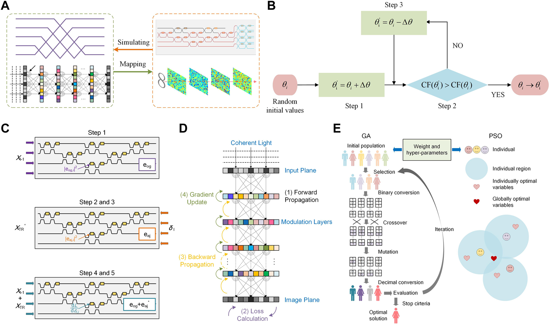
(A) The principle of the simulating and mapping (S&M) method. (B) The workflow of the forward propagation method for in situ training of ONNs. (C) The workflow of in situ backpropagation and gradient measurement in MZI-based ONNs [157]. (D) The in situ training of diffractive optical neural networks via backpropagation [159]. (E) The principle of in situ training of ONNs via neuroevolution [161].
Forward propagation is a kind of in-situ training method that is suitable for ONNs which are easy to implement the forward propagation and detection process, and easy to program/adjust the weight parameters. We take the MZI-based ONNs as an example and depict its training workflow in Figure 6B. For MZI-based ONNs, the related weight parameters are the phases of the internal and external phase shifter of MZI. Firstly, all phases of MZIs of the network are randomly initialized. Then in step 1, a specified phase θi is adjusted to θi’ = θi + Δθ with a small phase shift Δθ. Benefitting from the ultra-fast speed of forward propagation, the cost function can be rapidly calculated before and after adjusting. If the cost function CF(θi’) related to θi’ decreases compared to that of θi in step 2, then the θi is updated to θi’. Otherwise, the θi is adjusted to θi’ = θi − Δθ within step 3 and redoing the step 2. After processing the step 2 and step 3 for θi, other phases successively perform the same procedure. When all phases finished the procedure from step 1 to step 3, the traversal of all phases is performed repeatedly until the cost function converges. Ref. [44] firstly proposed that MZI-based ONNs can implement the on-chip training by using the forward propagation and the finite difference method, and implemented a simulation on a computer. It should be noted that this method is not favoured on a computer as the computation expense of forward-propagation (massive MVM calculation) is very high. After that, Ref. [102] demonstrated the self-configuring on a reconfigurable silicon photonic signal processor by using the forward propagation method. The silicon processor was consisted of a 4 × 4 MZI-network derived from Reck design [97] and can implement the linear transformation and nonnegative MVM operation [158]. The self-configured processor realized various optical signal processing functions, including multichannel optical switching, optical multiple-input-multiple-output descrambler, and tunable optical filter. In 2018, Hughes et al. proposed a highly efficient, in-situ training method for ONNs through adjoint variable methods to derive the photonic analogue of the backpropagation algorithm [157]. The workflow of the in-situ backpropagation and gradient measurement method is depicted in Figure 6C. In step 1, the original field amplitudes Xl-1 were input into the network and the intensities at each phase shifter were stored as eog. Then sending the adjoint mode amplitudes δl through the output port to record the XTR* from the input port and the intensities eaj at each phase shifter in step 2 and step 3. Next, calculated time-reversed adjoint input field amplitudes and the original field amplitudes Xl-1 were both input the device and measuring again the resulting intensities eog + eaj* at each phase shifter. In the end, the gradient of the cost function versus the weight parameters (permittivity of phase shifter) was recovered by subtracting the constant intensity terms from steps 1 and 2 and multiply by k02. By using the backpropagation, all weight parameters can be updated simultaneously in once iteration, which was highly efficient compared to that of the forward propagation method. Besides, Zhou et al. also demonstrated that the gradient of the cost function with respect to the weights of diffractive layers can be accurately calculated by measuring the forward and backward propagated optical fields in D2NN [159]. The principle of the in-situ training method of diffractive ONNs is shown in Figure 6D. At first, the coherent light was modulated and then forward propagated through multilayer SLMs with phase modulation coefficients, then the forward propagated optical field was measured by the image sensors with phase-shifted reference beams at the output image plane as well as at the individual layers. Next, the error optical field was calculated from the residual errors between the network output optical field and the ground truth label. Further, the backward propagated optical field was measured by propagating the error optical field from the output image plane back to the input plane. Based on the measured forward and backward propagated optical fields, the gradients of the diffractive layers can be calculated, and the modulation coefficients of SLMs were successively updated from the last to first layer. Finally, the in-situ optical training of a 10-layer diffractive ONN for MNIST dataset realized the blind testing accuracy of 92.19% and 91.96% without and with errors, respectively. Expect for measuring the gradient to minimize the cost function, gradient-free algorithms can be utilized to train ANNs [160–162]. In 2019, Zhang et al. proposed using neuroevolution algorithms to efficiently train ONNs on an on-chip integration system [161]. Two typically evolutionary algorithms, genetic algorithms (GA) and particle swarm optimization (PSO) were demonstrated to determine the hyper-parameters of ONNs and to optimize the weights (phase shifters) in the MZI-based ONN. The flowcharts of the learning algorithms for the ONNs based on GA and PSO are depicted in Figure 6E. In the preparation stage, multiple individuals and particles were randomly generated for GA’s initial population and PSO’s initial location, respectively, where each individual/particle encoded the information of the weights and the hyper-parameters of N layers ONN. Then, the fitness of individuals/particles was calculated by configuring their parameters on the device and calculating the cost function between the practical output and the ground truth. Based on the fitness and neuroevolution strategies, the new population of GA and new particles of PSO were updated. After that, re-evaluating the new population of GA and new particles of PSO and then re-evolving until the cost function converged or the iteration time reached maximum. In the end, the optimal configuration parameters of ONN were decoded from the optimal individual/particle. By the numerical training of MZI-based ONNs with the neuroevolution training method, the classification accuracies of GA for the test datasets were 97% (Iris plants dataset), 89% (wine dataset), and 92% (modulation format recognition dataset). And the classification accuracies of PSO for the test datasets were 100% (Iris plants dataset), 100% (wine dataset), and 93% (modulation format recognition dataset). Afterwards, Zhang et al. experimentally demonstrated the in-situ training of MZI-based ONNs with GA on an integrated hybrid optical processor [162]. And the proposed ONN obtained the highest accuracy of 94.2% on the training data set and 93.3% on the testing data set for Iris classification. In conclusion, due to the mature training algorithms in computers, the S&M method can quickly obtain the weight parameters of ONNs in advance and the difficulties in the experiment are avoided. But the environment noises and manufacturing errors may cause a decline to the accuracy of the practical ONNs. On the other hand, the in-situ training method can the real performance of the implementation of ONNs because the training process runs under the practical environment noises and manufacturing errors. Realizing the efficient and scalable in-situ training is one of the most promising directions in the future.
Discussion and outlook
In Chapter 2, we summarized various architectures and implementations in recent years for typical applications of analog optical computing, including the optical neural network (ONN), optical reservoir computing (ORC), and optical Ising machine (OIM). A large number of different types of ONNs have been proposed based on different optics platforms (integrated optics, free space optics, and fiber optics) and optical phenomena (interference, diffraction, nonlinearity and so on). Then, we introduced the common optical nonlinearity activation functions and training algorithms in analog optical computing. Here, we will discuss the current challenges of analog optical computing and the possible development directions in the future.
The potential and advantage of using optics to implement computation have been demonstrated [18, 33, 44, 48, 52, 55, 56, 63, 103, 121], which shows competitive performance with that of state-of-the-art electronic computing hardware. It should be noted that the current implementations of analog optical computing mainly focus on performing specific computation operations, e.g., dot product, MVM, convolution, and FT, and specific computation models, such as the neural network (NN) model, reservoir model, and Ising model. Besides, although the optical computing shows prominent advantage of negligible energy consumption when performing multiplication in optical domain. The modulation of the input signal, loading and maintaining the weights, detecting of the output signal, and performing the training algorithm are still highly dependent on the electronic equipment. Moreover, the computation module (mainly optical) and control/auxiliary module (mainly electrical) mostly are separated and the data flow in these computation systems is not optimized technically. In fact, the hybrid optoelectronic computing has been pointed out as the main existing form for analog optical computing [16, 26, 33, 38], which fully takes advantage of the low power consumption, high speed, and high parallelism of optical computing and the convenience of controlling of electronics, respectively. Thus, realizing a complete, highly efficient, and universal hybrid optoelectronic computing system is an important direction worth studying. In Ref. [123], Zhou et al. proposed to implement different computation models (DNNs, RNNs, weight-shared NNs) for large-scale neuromorphic optoelectronic computing by assembling diffractive processing units (DPUs) with different topological structures. It was a forward step to implement the universality of the optoelectronic computing system via reprogramming the basic computing unit. On the other hand, Shastri et al. depicted a blueprint for neuromorphic photonic processor architecture that adopted commercially available photonic packaging technology and some emerging ideas in the field of integrated photonics [38]. The concept of the neuromorphic photonic processor is shown in Figure 7A. It can be found that the system-in-package was consisted of on-chip laser source that provided carrier or generated optical frequency comb for ONNs, I/O that was compatible to optical signal, RF signal, and digital signal for modulators and detectors, the COMS application-specific integrated circuit (ASIC) that was used to drive/configure the photonic elements of photonic integrated circuit, digital memory (volatile, RAM) and analog memory (non-volatile), microcontroller, CPU and so on. The realization of this system-in-package depended on the fusion of advanced photonics and packaging technologies, for instance, active on-chip electronics, on-chip light sources, Lithium niobate-on-insulator modulators, and optical frequency combs. This blueprint provided us a promising way to fully exploit the advantage of photonics for accelerating computation in system level. Besides, Demirkiran et al. proposed an electro-photonic system for accelerating DNNs in system-level perspective [163]. The electro-photonic system consisting of an electronic host processor, dynamic random-access memory (DRAM), and a custom electro-photonic hardware accelerator called ADEPT is depicted in Figure 7B. In ADEPT, the photo-core was used to implement the dominant general matrix-matrix multiplication (GEMM) and a digital electronic ASIC was used for storage and for performing non-GEMM operations. The host CPU combined with DRAM performed the data scheduling via the PCI-e port connected with weight static random-access memory (SRAM) and activation SRAM. To improve the operational efficiency, the pipeline operation was adopted for GEMM and non-GEMM operations, and an optimized buffering method was used to maximize the batch size stored in the activation SRAM without ever spilling back to the DRAM during runtime. By a head-to-head comparison of ADEPT with systolic array architectures, the ADEPT can provide, on average, 7.19× higher inference throughput per watt. Besides, Sunny et al. proposed a novel cross-layer optimized neural network accelerator called CrossLight [164]. In the device-level, the MRR for performing the NN computation was optimized to be more resilient to process variations and thermal crosstalk; In circuit-level, an enhanced tuning circuit was proposed to simultaneously support large thermal-induced resonance shifts and high-speed device tuning; In architecture-level, the WDM technology and matrix decomposition were optimized to increase throughput and energy-efficiency. Based on the deep-level optimization, CrossLight can support 9.5× lower energy-per-bit and 15.9× higher performance-per-watt than state-of-the-art photonic deep learning accelerators. It can be found that the computation power of the hybrid optoelectronic computing system not only depends on the photonic computing core, but also depends on the highly efficient fusion of electronics and optics at the system level and architecture level. Thus, the high-efficiency hybrid optoelectronic computing architecture is an important studying direction in the future.
FIGURE 7
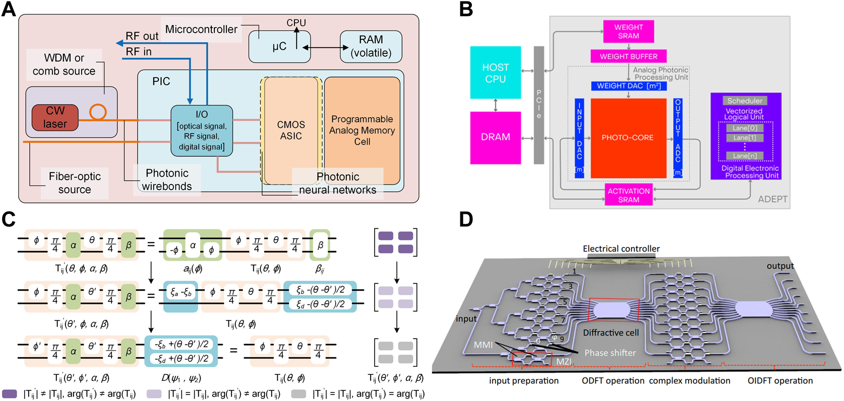
(A) The concept of the neuromorphic photonic processor with commercially available photonic packaging technology and some emerging ideas in the field of integrated photonics [38]. (B) The schematic and workflow of an electro-photonic computing system [163]. (C) The principle of the hardware error correction in large-scale MZI networks [165]. (D) The schematic of the space-efficient optical integrated diffractive neural networks [103]. (B) Reprinted from Ref. 163 with permission from arXiv preprint. (D) Reprinted from Ref. 103 with permission from Springer Nature: Nature Communications.
Due to the natural parallelism of light, analog optical computing would show bigger advantage as the scale of parallel computing, i.e., the scale of matrix/vector. However, some methods for implementing the MVM suffer from the extension of scale due to the fabrication error, especially in coherent integrated platform. As Refs. [46, 98, 111, 165] demonstrated, affected by the fabrication error of the splitting ratio and phase error in MZI, the fidelity of the unitary matrix represented by the MZI network and the classification accuracy of MZI-based ONNs sharply decreased with the growing of the number of modes. Thus, improving the robustness of the analog optical computing architecture to the fabrication error is also crucial. In Ref. [46], the MZI network for representing unitary matrix based on SVD was simplified into the more compact FFTNet based on Cooley-Tukey FFT algorithm [166]. With fewer components and shallower optical depth, the ONNs constructed by FFTNet demonstrated better fault tolerance to the error of components compared to that of SVD method. Afterwards, Ref. [103] also proved that the FFT-based ONNs can provide a ∼10-fold reduction in both footprint and energy consumption, as well as equal high accuracy with previous MZI-based ONNs. Besides, more robust architectures for programmable universal unitary have been developed in recent years. In Ref. [111], the unitary matrix was decomposed into multiple mode mixing layers and phase layers, where the transfer matrix of the mixing layer can be arbitrary unitary matrix. Even if adding random perturbations to the mode mixing layers, the fidelity of the unitary matrix can reach a high level, which demonstrated the resilience of its architecture to practical constraints and errors. In Refs. [108, 110, 167], multiport directional couplers (MDCs) were used to implement the mode mixing to realize multi-input-multi-output (MIMO) demultiplexing, unitary optical processor, and unitary converter. Compared to the optical unitary converter based on MZI, the MDC-based optical unitary converter showed outstanding robustness against waveguide deviations and fabrication errors. Moreover, Bandyopadhyay et al. proposed an optimization approach to correcting circuit errors in MZI network by locally correcting hardware errors within individual optical gates [165]. The procedure of correcting method is depicted in Figure 7C. The realistic MZI implemented on a photonics platform leaded to splitting errors α, β for the two directional couplers within the interferometer. At first, the θ was corrected to set the magnitudes of the elements of the realistic unitary matrix Tij’ equal to that of the target unitary matrix Tij. Then, the phase corrections were implemented to the input and outputs of the device to correct phase errors between Tij and Tij’. With this correction, the ONNs remained resilient to component error well beyond modern day process tolerances without using additional components. This method pointed out a potential way to scale up programmable photonics to hundreds of modes with current fabrication processes. In conclusion, the scalability and robustness of the analog optical computing architecture are important criteria worth being explored in the future with fewer components, compact structures, calibration schemes and so on.
Apart from the innovation at the system-level and architecture-level, the development of the underlying photonics devices and the application of advanced manufacturing process are also critical. In early stage, the lens system is used to implement FT and convolution. However, this equipment is bulky so that it is hard for extension and integration. Ref. [103] proposed using diffractive cells (slab waveguides) shown in Figure 7D as equivalent lens to implement FT. Due to the ultracompact footprint of diffractive cell, the footprint and energy consumption of the integrated ONNs greatly reduced. Ref. [168] inversely designed an integrated-nanophotonics computing unit consisting of a multimode interference (MMI) coupler with nanopatterned coupler region to implement the parallel convolution. Moreover, Ref. [169] proposed an integrated ONN based on on-chip cascaded one-dimensional metalines, which can perform MVM in parallel and with low energy consumption due to intrinsic parallelism and low-loss of silicon metalines. Meanwhile, Ref. [125] proposed integrated diffractive neural networks enabled by metasurface. Besides, Ref. [170] proposed a nanophotonic medium consisting of matrix material silicon dioxide and a large number of dopants to perform NN computing. The passive NN computing was implemented by light passing through the nanostructured medium with both linear and nonlinear scatterers. Based on these progresses, it can be found that the integration is a unified trend for analog optical computing. Driven by the advanced material and integrated technique in optoelectronics, analog optical computing will play an essential role in the post-Moore era.
Conclusion
In this paper, we systematically review and discuss the advanced field—analog optical computing in different aspects. Firstly, we introduce the challenges of the modern electronic computing in the post-Moore era, with slowing down of Moore’s law and growing demands of massive data processing, analog optical computing becomes a promising way to break through the bottlenecks of electronics. Then, the recent processes of analog optical computing are summarized by dividing its implementations into four typical optical platforms. Afterwards, the nonlinearity and training algorithm of analog optical computing are independently discussed in detail. At last, we point out the current challenges and potential development directions in the future. It can be seen from the development history that the integration of computing architectures is a distinct direction to fully liberate the computing power for optical computing. At the same time, due to the complementary advantages of electronics and optics, the optimization of the hybrid optoelectronic computing is also crucial. Besides, the new materials and advanced manufacturing process also play an important role to explore the limits of performance of analog optical computing. It is believed the analog optical computing has a promising prospect in the post-Moore era by the improvement of optoelectronic technology and photonic integrated circuits.
Statements
Author contributions
YD and TZ contributed to conception and guided the research. YD wrote the first draft of the manuscript. ZF, QC, and YL wrote sections of the manuscript. YD, TZ, XS, and KX contributed to manuscript revision. All authors commented on the manuscript and approved the submitted version.
Funding
This work was supported by the National Natural Science Foundation of China (62171055, 61705015, 61625104, 61821001, 62135009, 61971065); Fund of State Key Laboratory of Information Photonics and Optical Communications (BUPT) (IPOC2020ZT08, IPOC2020ZT03), P.R. China; National Key Research and Development Program of China (2019YFB1803504).
Conflict of interest
The authors declare that the research was conducted in the absence of any commercial or financial relationships that could be construed as a potential conflict of interest.
Publisher’s note
All claims expressed in this article are solely those of the authors and do not necessarily represent those of their affiliated organizations, or those of the publisher, the editors and the reviewers. Any product that may be evaluated in this article, or claim that may be made by its manufacturer, is not guaranteed or endorsed by the publisher.
References
1.
McCulloch WS Pitts W . A logical calculus of the ideas immanent in nervous activity. Bull Math Biophys (1943) 5(4):115–33. 10.1007/BF02478259
2.
Hinton GE Osindero S Teh Y-W . A fast learning algorithm for deep belief nets. Neural Comput (2006) 18(7):1527–54. 10.1162/neco.2006.18.7.1527
3.
Kitayama K Notomi M Naruse M Inoue K Kawakami S Uchida A . Novel frontier of photonics for data processing—photonic accelerator. APL Photon (2019) 4(9):090901. 10.1063/1.5108912
4.
Shawahna A Sait SM El-Maleh A . Fpga-based accelerators of deep learning networks for learning and classification: A review. IEEE Access (2019) 7:7823–59. 10.1109/access.2018.2890150
5.
Machupalli R Hossain M Mandal M . Review of asic accelerators for deep neural network. Microprocessors and Microsystems (2022) 89:104441. 10.1016/j.micpro.2022.104441
6.
Tan T Cao G . Fastva: Deep learning video analytics through edge processing and npu in mobile. In: IEEE Conference on Computer Communications. IEEE (2020). p. 1947–56.
7.
Furber SB Lester DR Plana LA Garside JD Painkras E Temple S et al Overview of the spinnaker system Architecture. IEEE Trans Comput (2013) 62(12):2454–67. 10.1109/TC.2012.142
8.
Benjamin BV Gao P McQuinn E Choudhary S Chandrasekaran AR Bussat J-M et al Neurogrid: A mixed-analog-digital multichip system for large-scale neural simulations. Proc IEEE (2014) 102(5):699–716. 10.1109/jproc.2014.2313565
9.
Merolla PA Arthur JV Alvarez-Icaza R Cassidy AS Sawada J Akopyan F et al A million spiking-neuron integrated circuit with a scalable communication network and interface. Science (2014) 345(6197):668–73. 10.1126/science.1254642
10.
Davies M Srinivasa N Lin T-H Chinya G Cao Y Choday SH et al Loihi: A neuromorphic manycore processor with on-chip learning. IEEE Micro (2018) 38(1):82–99. 10.1109/MM.2018.112130359
11.
Pei J Deng L Song S Zhao M Zhang Y Wu S et al Towards artificial general intelligence with hybrid tianjic chip architecture. Nature (2019) 572(7767):106–11. 10.1038/s41586-019-1424-8
12.
Dennard RH Gaensslen FH Yu H-N Rideout VL Bassous E LeBlanc AR . Design of ion-implanted mosfet's with very small physical dimensions. IEEE J Solid-state Circuits (1974) 9(5):256–68. 10.1109/JSSC.1974.1050511
13.
Waldrop MM . The chips are down for Moore’s law. Nature (2016) 530(7589):144–7. 10.1038/530144a
14.
Miller DAB . Device requirements for optical interconnects to silicon chips. Proc IEEE (2009) 97(7):1166–85. 10.1109/jproc.2009.2014298
15.
Nahmias MA de Lima TF Tait AN Peng H-T Shastri BJ Prucnal PR . Photonic multiply-accumulate operations for neural networks. IEEE J Sel Top Quan Electron (2020) 26(1):1–18. 10.1109/jstqe.2019.2941485
16.
Li C Zhang X Li J Fang T Dong X . The challenges of modern computing and new opportunities for optics. PhotoniX (2021) 2(1):20. 10.1186/s43074-021-00042-0
17.
Karpov M Pfeiffer MHP Guo H Weng W Liu J Kippenberg TJ . Dynamics of soliton crystals in optical microresonators. Nat Phys (2019) 15(10):1071–7. 10.1038/s41567-019-0635-0
18.
Xu X Tan M Corcoran B Wu J Boes A Nguyen TG et al 11 tops photonic convolutional accelerator for optical neural networks. Nature (2021) 589(7840):44–51. 10.1038/s41586-020-03063-0
19.
Tsai F-CF O’Brien CJ Petrovic´ NS Rakic´ AD . Analysis of optical channel cross talk for free-space optical interconnects in the presence of higher-order transverse modes. Appl Opt (2005) 44(30):6380–7. 10.1364/AO.44.006380
20.
Miller DAB . Waves, modes, communications, and optics: A tutorial. Adv Opt Photon (2019) 11(3):679–825. 10.1364/aop.11.000679
21.
Goodman JW Leonberger FJ Kung S-Y Athale RA . Optical interconnections for vlsi systems. Proc IEEE (1984) 72(7):850–66. 10.1109/PROC.1984.12943
22.
Miller DAB . Rationale and challenges for optical interconnects to electronic chips. Proc IEEE (2000) 88(6):728–49. 10.1109/5.867687
23.
Miller DAB . Attojoule optoelectronics for low-energy information processing and communications. J Lightwave Technol (2017) 35(3):346–96. 10.1109/jlt.2017.2647779
24.
Huang C Sorger VJ Miscuglio M Al-Qadasi M Mukherjee A Lampe L et al Prospects and applications of photonic neural networks. Adv Phys X (2021) 7(1):1981155. 10.1080/23746149.2021.1981155
25.
Touch J Badawy A-H Sorger VJ . Optical computing. Nanophotonics (2017) 6(3):503–5. 10.1515/nanoph-2016-0185
26.
Bai B Shu H Wang X Zou W . Towards silicon photonic neural networks for artificial intelligence. Sci China Inf Sci (2020) 63(6):160403. 10.1007/s11432-020-2872-3
27.
Ambs P . Optical computing: A 60-year adventure. Adv Opt Tech (2010) 2010:1–15. 10.1155/2010/372652
28.
Caulfield HJ Dolev S . Why future supercomputing requires optics. Nat Photon (2010) 4(5):261–3. 10.1038/nphoton.2010.94
29.
Jain K Pratt GW . Optical transistor. Appl Phys Lett (1976) 28(12):719–21. 10.1063/1.88627
30.
Touch J Cao Y Ziyadi M Almaiman A Mohajerin-Ariaei A Willner AE . Digital optical processing of optical communications: Towards an optical turing machine. Nanophotonics (2017) 6(3):507–30. 10.1515/nanoph-2016-0145
31.
Sawchuk AA Strand TC . Digital optical computing. Proc IEEE (1984) 72(7):758–79. 10.1109/PROC.1984.12937
32.
Miller DAB . Are optical transistors the logical next step?Nat Photon (2010) 4(1):3–5. 10.1038/nphoton.2009.240
33.
Wetzstein G Ozcan A Gigan S Fan S Englund D Soljacic M et al Inference in artificial intelligence with deep optics and photonics. Nature (2020) 588(7836):39–47. 10.1038/s41586-020-2973-6
34.
Thomson D Zilkie A Bowers JE Komljenovic T Reed GT Vivien L et al Roadmap on silicon photonics. J Opt (2016) 18(7):073003. 10.1088/2040-8978/18/7/073003
35.
Wang X Liu J . Emerging technologies in Si active photonics. J Semicond (2018) 39(6):061001. 10.1088/1674-4926/39/6/061001
36.
Zhou H Dong J Cheng J Dong W Huang C Shen Y et al Photonic matrix multiplication lights up photonic accelerator and beyond. Light Sci Appl (2022) 11(1):30. 10.1038/s41377-022-00717-8
37.
Peng H-T Nahmias MA Lima TF Tait AN Shastri BJ Prucnal PR . Neuromorphic photonic integrated circuits. IEEE J Sel Top Quan Electron (2018) 24(6):1–15. 10.1109/jstqe.2018.2840448
38.
Shastri BJ Tait AN Lima TF Pernice WHP Bhaskaran H Wright CD et al Photonics for artificial intelligence and neuromorphic computing. Nat Photon (2021) 15(2):102–14. 10.1038/s41566-020-00754-y
39.
Liu J Wu Q Sui X Chen Q Gu G Wang L et al Research progress in optical neural networks: Theory, applications and developments. PhotoniX (2021) 2(1):5. 10.1186/s43074-021-00026-0
40.
Xu S Wang J Shu H Zhang Z Yi S Bai B et al Optical coherent dot-product chip for sophisticated deep learning regression. Light Sci Appl (2021) 10(1):221. 10.1038/s41377-021-00666-8
41.
Miscuglio M Sorger VJ . Photonic tensor cores for machine learning. Appl Phys Rev (2020) 7(3):031404. 10.1063/5.0001942
42.
Goodman JW Dias AR Woody LM . Fully parallel, high-speed incoherent optical method for performing discrete fourier transforms. Opt Lett (1978) 2(1):1–3. 10.1364/OL.2.000001
43.
Yang L Ji R Zhang L Ding J Xu Q . On-chip cmos-compatible optical signal processor. Opt Express (2012) 20(12):13560–5. 10.1364/OE.20.013560
44.
Shen Y Harris NC Skirlo S Prabhu M Baehr-Jones T Hochberg M et al Deep learning with coherent nanophotonic circuits. Nat Photon (2017) 11(7):441–6. 10.1038/nphoton.2017.93
45.
Bieren K . Lens design for optical fourier transform systems. Appl Opt (1971) 10(12):2739–42. 10.1364/AO.10.002739
46.
Fang MYS Manipatruni S Wierzynski C Khosrowshahi A DeWeese MR . Design of optical neural networks with component imprecisions. Opt Express (2019) 27(10):14009–29. 10.1364/oe.27.014009
47.
Chang J Sitzmann V Dun X Heidrich W Wetzstein G . Hybrid optical-electronic convolutional neural networks with optimized diffractive optics for image classification. Sci Rep (2018) 8(1):12324. 10.1038/s41598-018-30619-y
48.
Feldmann J Youngblood N Karpov M Gehring H Li X Stappers M et al Parallel convolutional processing using an integrated photonic tensor core. Nature (2021) 589(7840):52–8. 10.1038/s41586-020-03070-1
49.
Inagaki T Inaba K Hamerly R Inoue K Yamamoto Y Takesue H . Large-scale ising spin network based on degenerate optical parametric oscillators. Nat Photon (2016) 10(6):415–9. 10.1038/nphoton.2016.68
50.
Vandoorne K Mechet P Van Vaerenbergh T Fiers M Morthier G Verstraeten D et al Experimental demonstration of reservoir computing on a silicon photonics chip. Nat Commun (2014) 5(1):3541. 10.1038/ncomms4541
51.
Zhang H Gu M Jiang XD Thompson J Cai H Paesani S et al An optical neural chip for implementing complex-valued neural network. Nat Commun (2021) 12(1):457. 10.1038/s41467-020-20719-7
52.
Ashtiani F Geers AJ Aflatouni F . An on-chip photonic deep neural network for image classification. Nature (2022) 606(1):501–6. 10.1038/s41586-022-04714-0
53.
Paquot Y Duport F Smerieri A Dambre J Schrauwen B Haelterman M et al Optoelectronic reservoir computing. Sci Rep (2012) 2(1):287. 10.1038/srep00287
54.
Borghi M Biasi S Pavesi L . Reservoir computing based on a silicon microring and time multiplexing for binary and analog operations. Sci Rep (2021) 11(1):15642. 10.1038/s41598-021-94952-5
55.
Roques-Carmes C Shen Y Zanoci C Prabhu M Atieh F Jing L et al Heuristic recurrent algorithms for photonic ising machines. Nat Commun (2020) 11(1):249. 10.1038/s41467-019-14096-z
56.
Prabhu M Roques-Carmes C Shen Y Harris N Jing L Carolan J et al Accelerating recurrent ising machines in photonic integrated circuits. Optica (2020) 7(5):551–8. 10.1364/optica.386613
57.
Abiodun OI Jantan A Omolara AE Dada KV Mohamed NA Arshad H . State-of-the-Art in artificial neural network applications: A survey. Heliyon (2018) 4(11):e00938. 10.1016/j.heliyon.2018.e00938
58.
Nahmias MA Shastri BJ Tait AN Prucnal PR . A leaky integrate-and-fire laser neuron for ultrafast cognitive computing. IEEE J Sel Top Quan Electron (2013) 19(5):1–12. 10.1109/jstqe.2013.2257700
59.
Carolin Mabel M Fernandez E . Analysis of wind power generation and prediction using ann: A case study. Renew Energ (2008) 33(5):986–92. 10.1016/j.renene.2007.06.013
60.
Min E Guo X Liu Q Zhang G Cui J Long J . A survey of clustering with deep learning: From the perspective of network architecture. IEEE Access (2018) 6:39501–14. 10.1109/access.2018.2855437
61.
Krizhevsky A Sutskever I Hinton GE . Imagenet classification with deep convolutional neural networks. Commun ACM (2017) 60(6):84–90. 10.1145/3065386
62.
LeCun Y Bengio Y Hinton G . Deep learning. Nature (2015) 521(7553):436–44. 10.1038/nature14539
63.
Lin X Rivenson Y Yardimci NT Veli M Luo Y Jarrahi M et al All-optical machine learning using diffractive deep neural networks. Science (2018) 361(6406):1004–8. 10.1126/science.aat8084
64.
Feldmann J Youngblood N Wright CD Bhaskaran H Pernice WHP . All-optical spiking neurosynaptic networks with self-learning capabilities. Nature (2019) 569(7755):208–14. 10.1038/s41586-019-1157-8
65.
Duport F Schneider B Smerieri A Haelterman M Massar S . All-optical reservoir computing. Opt Express (2012) 20(20):22783–95. 10.1364/OE.20.022783
66.
Coarer FD-L Sciamanna M Katumba A Freiberger M Dambre J Bienstman P et al All-optical reservoir computing on a photonic chip using silicon-based ring resonators. IEEE J Sel Top Quan Electron (2018) 24(6):1–8. 10.1109/jstqe.2018.2836985
67.
Maass W Natschlager T Markram H . Real-time computing without stable states: A new framework for neural computation based on perturbations. Neural Comput (2002) 14(11):2531–60. 10.1162/089976602760407955
68.
Jaeger H Haas H . Harnessing nonlinearity: Predicting chaotic systems and saving energy in wireless communication. Science (2004) 304(5667):78–80. 10.1126/science.1091277
69.
Brunner D Penkovsky B Marquez BA Jacquot M Fischer I Larger L . Tutorial: Photonic neural networks in delay systems. J Appl Phys (2018) 124(15):152004. 10.1063/1.5042342
70.
Schrauwen B Verstraeten D Campenhout JV . An overview of reservoir computing: Theory, applications and implementations. Proc 15th Eur Symp Artif Neural networks (2007) 471–82.
71.
Tanaka G Yamane T Heroux JB Nakane R Kanazawa N Takeda S et al Recent advances in physical reservoir computing: A review. Neural Networks (2019) 115:100–23. 10.1016/j.neunet.2019.03.005
72.
Sande GV Brunner D Soriano MC . Advances in photonic reservoir computing. Nanophotonics (2017) 6(3):561–76. 10.1515/nanoph-2016-0132
73.
Brunner D Fischer I . Reconfigurable semiconductor laser networks based on diffractive coupling. Opt Lett (2015) 40(16):3854–7. 10.1364/OL.40.003854
74.
Bueno J Maktoobi S Froehly L Fischer I Jacquot M Larger L et al Reinforcement learning in a large-scale photonic recurrent neural network. Optica (2018) 5(6):756–60. 10.1364/optica.5.000756
75.
Dong J Rafayelyan M Krzakala F Gigan S . Optical reservoir computing using multiple light scattering for chaotic systems prediction. IEEE J Sel Top Quan Electron (2020) 26(1):1–12. 10.1109/jstqe.2019.2936281
76.
Rafayelyan M Dong J Tan Y Krzakala F Gigan S . Large-scale optical reservoir computing for spatiotemporal chaotic systems prediction. Phys Rev X (2020) 10(4):041037. 10.1103/PhysRevX.10.041037
77.
Paudel U Luengo-Kovac M Pilawa J Shaw TJ Valley GC . Classification of time-domain waveforms using a speckle-based optical reservoir computer. Opt Express (2020) 28(2):1225–37. 10.1364/OE.379264
78.
Larger L Soriano MC Brunner D Appeltant L Gutierrez JM Pesquera L et al Photonic information processing beyond turing: An optoelectronic implementation of reservoir computing. Opt Express (2012) 20(3):3241–9. 10.1364/OE.20.003241
79.
Takano K Sugano C Inubushi M Yoshimura K Sunada S Kanno K et al Compact reservoir computing with a photonic integrated circuit. Opt Express (2018) 26(22):29424–39. 10.1364/OE.26.029424
80.
Papadimitriou CH Steiglitz K . Combinatorial optimization: Algorithms and complexity. North Chelmsford: Courier Corporation (1998).
81.
RaymondMiller EJWT Bohlinger JD , editors. Complexity of computer computations. Plenum Press (1972).
82.
Lucas A . Ising formulations of many Np problems. Front Phys (2014) 2:5. 10.3389/fphy.2014.00005
83.
Koenderink AF Alù A Polman A . Nanophotonics: Shrinking light-based technology. Science (2015) 348(6234):516–21. 10.1126/science.1261243
84.
Inagaki T Haribara Y Igarashi K Sonobe T Tamate S Honjo T et al A coherent ising machine for 2000-node optimization problems. Science (2016) 354(6312):603–6. 10.1126/science.aah4243
85.
McMahon PL Marandi A Haribara Y Hamerly R Langrock C Tamate S et al A fully-programmable 100-spin coherent ising machine with all-to-all connections. Science (2016) 354(6312):614–7. 10.1126/science.aah5178
86.
Babaeian M Nguyen DT Demir V Akbulut M Blanche PA Kaneda Y et al A single shot coherent ising machine based on a network of injection-locked multicore fiber lasers. Nat Commun (2019) 10(1):3516. 10.1038/s41467-019-11548-4
87.
Pierangeli D Marcucci G Conti C . Large-scale photonic ising machine by spatial light modulation. Phys Rev Lett (2019) 122(21):213902. 10.1103/PhysRevLett.122.213902
88.
Pierangeli D Marcucci G Conti C . Adiabatic evolution on a spatial-photonic ising machine. Optica (2020) 7(11):1535–43. 10.1364/optica.398000
89.
Soref R . The past, present, and future of silicon photonics. IEEE J Sel Top Quan Electron (2006) 12(6):1678–87. 10.1109/jstqe.2006.883151
90.
Siew SY Li B Gao F Zheng HY Zhang W Guo P et al Review of silicon photonics technology and platform development. J Lightwave Technol (2021) 39(13):4374–89. 10.1109/jlt.2021.3066203
91.
Liao L Samara-Rubio D Morse M Liu A Hodge D Rubin D et al High speed silicon mach-zehnder modulator. Opt Express (2005) 13(8):3129–35. 10.1364/OPEX.13.003129
92.
Amin R Maiti R Carfano C Ma Z Tahersima MH Lilach Y et al 0.52 V mm ITO-based Mach-Zehnder modulator in silicon photonics. APL Photon (0201) 3(12):126104. 10.1063/1.5052635
93.
Fu Y Hu X Gong Q . Silicon photonic crystal all-optical logic gates. Phys Lett A (2013) 377(3-4):329–33. 10.1016/j.physleta.2012.11.034
94.
Fan W Jianyi Y Limei C Xiaoqing J Minghua W . Optical switch based on multimode interference coupler. IEEE Photon Technol Lett (2006) 18(2):421–3. 10.1109/lpt.2005.863201
95.
Kiyat I Aydinli A Dagli N . A compact silicon-on-insulator polarization splitter. IEEE Photon Technol Lett (2005) 17(1):100–2. 10.1109/lpt.2004.838133
96.
Deng Q Yan Q Liu L Li X Michel J Zhou Z . Robust polarization-insensitive strip-slot waveguide mode converter based on symmetric multimode interference. Opt Express (2016) 24(7):7347–55. 10.1364/OE.24.007347
97.
Reck M Zeilinger A Bernstein HJ Bertani P . Experimental realization of any discrete unitary operator. Phys Rev Lett (1994) 73(1):58–61. 10.1103/PhysRevLett.73.58
98.
Pai S Bartlett B Solgaard O Miller DAB . Matrix optimization on universal unitary photonic devices. Phys Rev Appl (2019) 11(6):064044. 10.1103/PhysRevApplied.11.064044
99.
Ribeiro A Ruocco A Vanacker L Bogaerts W . Demonstration of a 4 × 4-port universal linear circuit. Optica (2016) 3(12):1348–57. 10.1364/optica.3.001348
100.
Clements WR Humphreys PC Metcalf BJ Kolthammer WS Walsmley IA . Optimal design for universal multiport interferometers. Optica (2016) 3(12):1460–5. 10.1364/optica.3.001460
101.
Harris NC Steinbrecher GR Prabhu M Lahini Y Mower J Bunandar D et al Quantum transport simulations in a programmable nanophotonic processor. Nat Photon (2017) 11(7):447–52. 10.1038/nphoton.2017.95
102.
Zhou H Zhao Y Wang X Gao D Dong J Zhang X . Self-configuring and reconfigurable silicon photonic signal processor. ACS Photon (2020) 7(3):792–9. 10.1021/acsphotonics.9b01673
103.
Zhu HH Zou J Zhang H Shi YZ Luo SB Wang N et al Space-efficient optical computing with an integrated chip diffractive neural network. Nat Commun (2022) 13(1):1044. 10.1038/s41467-022-28702-0
104.
Tian Y Zhao Y Liu S Li Q Wang W Feng J et al Scalable and compact photonic neural chip with low learning-capability-loss. Nanophotonics (2022) 11(2):329–44. 10.1515/nanoph-2021-0521
105.
Miller DAB . Self-aligning universal beam coupler. Opt Express (2013) 21(5):6360–70. 10.1364/OE.21.006360
106.
Miller DAB . Self-configuring universal linear optical component [Invited]. Photon Res (2013) 1(1):1–15. 10.1364/prj.1.000001
107.
Barak R Ben-Aryeh Y . Quantum fast fourier transform and quantum computation by linear optics. J Opt Soc Am B (2007) 24(2):231–40. 10.1364/JOSAB.24.000231
108.
Tang R Tanemura T Ghosh S Suzuki K Tanizawa K Ikeda K et al Reconfigurable all-optical on-chip mimo three-mode demultiplexing based on multi-plane light conversion. Opt Lett (2018) 43(8):1798–801. 10.1364/OL.43.001798
109.
Tanomura R Tang R Ghosh S Tanemura T Nakano Y . Robust integrated optical unitary converter using multiport directional couplers. J Lightwave Technol (2020) 38(1):60–6. 10.1109/jlt.2019.2943116
110.
Tang R Tanomura R Tanemura T Nakano Y . Ten-port unitary optical processor on a silicon photonic chip. ACS Photon (2021) 8(7):2074–80. 10.1021/acsphotonics.1c00419
111.
Saygin MY Kondratyev IV Dyakonov IV Mironov SA Straupe SS Kulik SP . Robust architecture for programmable universal unitaries. Phys Rev Lett (2020) 124(1):010501. 10.1103/PhysRevLett.124.010501
112.
Nakajima M Tanaka K Hashimoto T . Scalable reservoir computing on coherent linear photonic processor. Commun Phys (2021) 4(1):20. 10.1038/s42005-021-00519-1
113.
Okawachi Y Yu M Jang JK Ji X Zhao Y Kim BY et al Demonstration of chip-based coupled degenerate optical parametric oscillators for realizing a nanophotonic spin-glass. Nat Commun (2020) 11(1):4119. 10.1038/s41467-020-17919-6
114.
Tait AN Nahmias MA Shastri BJ Prucnal PR . Broadcast and weight: An integrated network for scalable photonic spike processing. J Lightwave Technol (2014) 32(21):4029–41. 10.1109/jlt.2014.2345652
115.
Tait AN de Lima TF Zhou E Wu AX Nahmias MA Shastri BJ et al Neuromorphic photonic networks using silicon photonic weight banks. Sci Rep (2017) 7(1):7430. 10.1038/s41598-017-07754-z
116.
Cheng J Zhao Y Zhang W Zhou H Huang D Zhu Q et al A small microring array that performs large complex-valued matrix-vector multiplication. Front Optoelectron (2022) 15(1):15. 10.1007/s12200-022-00009-4
117.
Shi B Calabretta N Stabile R . Deep neural network through an inp soa-based photonic integrated cross-connect. IEEE J Sel Top Quan Electron (2020) 26(1):7701111–1. 10.1109/jstqe.2019.2945548
118.
Wu C Yu H Lee S Peng R Takeuchi I Li M . Programmable phase-change metasurfaces on waveguides for multimode photonic convolutional neural network. Nat Commun (2021) 12(1):96. 10.1038/s41467-020-20365-z
119.
Shi B Calabretta N Stabile R . Inp photonic integrated multi-layer neural networks: Architecture and performance analysis. APL Photon (2022) 7(1):010801. 10.1063/5.0066350
120.
Zuo Y Li B Zhao Y Jiang Y Chen Y-C Chen P et al All-optical neural network with nonlinear activation functions Optica (2019) 6(9):1132–7. 10.1364/optica.6.001132
121.
Wang T Ma SY Wright LG Onodera T Richard BC McMahon PL . An optical neural network using less than 1 photon per multiplication. Nat Commun (2022) 13(1):123. 10.1038/s41467-021-27774-8
122.
Yan T Wu J Zhou T Xie H Xu F Fan J et al Fourier-space diffractive deep neural network. Phys Rev Lett (2019) 123(2):023901. 10.1103/PhysRevLett.123.023901
123.
Zhou T Lin X Wu J Chen Y Xie H Li Y et al Large-scale neuromorphic optoelectronic computing with a reconfigurable diffractive processing unit. Nat Photon (2021) 15(5):367–73. 10.1038/s41566-021-00796-w
124.
Liu C Ma Q Luo ZJ Hong QR Xiao Q Zhang HC et al A programmable diffractive deep neural network based on a digital-coding metasurface array. Nat Electron (2022) 5(2):113–22. 10.1038/s41928-022-00719-9
125.
Luo X Hu Y Ou X Li X Lai J Liu N et al Metasurface-enabled on-chip multiplexed diffractive neural networks in the visible. Light Sci Appl (2022) 11(1):158. 10.1038/s41377-022-00844-2
126.
Athale RA Collin WС . Optical matrix-matrix multiplier based on outer product decomposition. Appl Opt (1982) 21(12):2089–90. 10.1364/AO.21.002089
127.
Yan T Yang R Zheng Z Lin X Xiong H Dai Q . All-optical graph representation learning using integrated diffractive photonic computing units. Sci Adv (2022) 8(24):eabn7630. 10.1126/sciadv.abn7630
128.
Yihang D Zhang T Sun X Dai J Xu K . Multifunctional plasmonic waveguide system based on coding metamaterials and inverse design. Opt Laser Technology (2022) 156:108478. 10.1016/j.optlastec.2022.108478
129.
Taillaert D Bienstman P Baets R . Compact efficient broadband grating coupler for silicon-on-insulator waveguides. Opt Lett (2004) 29(23):2749–51. 10.1364/OL.29.002749
130.
Dan Y Fan Z Sun X Zhang T Xu K . All-type optical logic gates using plasmonic coding metamaterials and multi-objective optimization. Opt Express (2022) 30(7):11633. 10.1364/oe.449280
131.
Dong P Shafiiha R Liao S Liang H Feng N-N Feng D et al Wavelength-tunable silicon microring modulator. Opt Express (2010) 18(11):10941–6. 10.1364/OE.18.010941
132.
Bach HG Beling A Mekonnen GG Kunkel R Schmidt D Ebert W et al Inp-based waveguide-integrated photodetector with 100-ghz bandwidth. IEEE J Sel Top Quan Electron (2004) 10(4):668–72. 10.1109/jstqe.2004.831510
133.
Komljenovic T Huang D Pintus P Tran MA Davenport ML Bowers JE . Photonic integrated circuits using heterogeneous integration on silicon. Proc IEEE (2018) 106(12):2246–57. 10.1109/JPROC.2018.2864668
134.
Lee KH Wang Y Wang B Zhang L Sasangka WA Bao S et al Monolithic integration of Si-cmos and iii-V-on-Si through direct wafer bonding process. IEEE J Electron Devices Soc (2017) 6:571–8. 10.1109/JEDS.2017.2787202
135.
Zang Y Chen M Yang S Chen H . Electro-optical neural networks based on time-stretch method. IEEE J Sel Top Quan Electron (2020) 26(1):1–10. 10.1109/jstqe.2019.2957446
136.
Appeltant L Soriano MC Van der Sande G Danckaert J Massar S Dambre J et al Information processing using a single dynamical node as complex system. Nat Commun (2011) 2(1):468. 10.1038/ncomms1476
137.
Brunner D Soriano MC Mirasso CR Fischer I . Parallel photonic information processing at gigabyte per second data rates using transient states. Nat Commun (2013) 4:1364. 10.1038/ncomms2368
138.
Dejonckheere A Duport F Smerieri A Fang L Oudar J-L Haelterman M et al All-optical reservoir computer based on saturation of absorption. Opt Express (2014) 22(9):10868–81. 10.1364/oe.22.010868
139.
Teo TY Ma X Pastor E Wang H George JK Yang JKW et al Programmable chalcogenide-based all-optical deep neural networks. Nanophotonics (2022) 11(17):4073–88. 10.1515/nanoph-2022-0099
140.
Amin R George JK Sun S Ferreira de Lima T Tait AN Khurgin JB et al Ito-based electro-absorption modulator for photonic neural activation function. APL Mater (2019) 7(8):081112. 10.1063/1.5109039
141.
George JK Mehrabian A Amin R Meng J de Lima TF Tait AN et al Neuromorphic photonics with electro-absorption modulators. Opt Express (2019) 27(4):5181–91. 10.1364/OE.27.005181
142.
Tait AN Ferreira de Lima T Nahmias MA Miller HB Peng H-T Shastri BJ et al Silicon photonic modulator neuron. Phys Rev Appl (2019) 11(6):064043. 10.1103/PhysRevApplied.11.064043
143.
Williamson IAD Hughes TW Minkov M Bartlett B Pai S Fan S . Reprogrammable electro-optic nonlinear activation functions for optical neural networks. IEEE J Sel Top Quan Electron (2020) 26(1):1–12. 10.1109/jstqe.2019.2930455
144.
Pour Fard MM Williamson IAD Edwards M Liu K Pai S Bartlett B et al Experimental realization of arbitrary activation functions for optical neural networks. Opt Express (2020) 28(8):12138–48. 10.1364/OE.391473
145.
Miscuglio M Mehrabian A Hu Z Azzam SI George J Kildishev AV et al All-optical nonlinear activation function for photonic neural networks [Invited]. Opt Mater Express (2018) 8(12):3851–63. 10.1364/ome.8.003851
146.
Mourgias-Alexandris G Tsakyridis A Passalis N Tefas A Vyrsokinos K Pleros N . An all-optical neuron with sigmoid activation function. Opt Express (2019) 27(7):9620–30. 10.1364/OE.27.009620
147.
Jha A Huang C Prucnal PR . Reconfigurable all-optical nonlinear activation functions for neuromorphic photonics. Opt Lett (2020) 45(17):4819–22. 10.1364/OL.398234
148.
Mourgias-Alexandris G Dabos G Passalis N Totovic A Tefas A Pleros N . All-optical wdm recurrent neural networks with gating. IEEE J Sel Top Quan Electron (2020) 26(5):1–7. 10.1109/jstqe.2020.2995830
149.
Huang C Jha A de Lima TF Tait AN Shastri BJ Prucnal PR . On-chip programmable nonlinear optical signal processor and its applications. IEEE J Sel Top Quan Electron (2021) 27(2):6100211–1. 10.1109/jstqe.2020.2998073
150.
Ryou A Whitehead J Zhelyeznyakov M Anderson P Keskin C Bajcsy M et al Free-space optical neural network based on thermal atomic nonlinearity. Photon Res (2021) 9(4):B128–B34. 10.1364/prj.415964
151.
de Lima TF Tait AN Saeidi H Nahmias MA Peng H-T Abbaslou S et al Noise analysis of photonic modulator neurons. IEEE J Sel Top Quan Electron (2020) 26(1):1–9. 10.1109/jstqe.2019.2931252
152.
Shastri BJ Nahmias MA Tait AN Rodriguez AW Wu B Prucnal PR . Spike processing with a graphene excitable laser. Sci Rep (2016) 6:19126. 10.1038/srep19126
153.
Rasmussen TS Yu Y Mork J . All-optical non-linear activation function for neuromorphic photonic computing using semiconductor Fano lasers. Opt Lett (2020) 45(14):3844–7. 10.1364/OL.395235
154.
Soljacˇic´ M Ibanescu M Johnson SG Fink Y Joannopoulos JD . Optimal bistable switching in nonlinear photonic crystals. Phys Rev E (2002) 66(5):055601. 10.1103/PhysRevE.66.055601
155.
Razeghi M Tournié E Brown GJ Mesaritakis C Kapsalis A Syvridis D , editors. All-optical reservoir computing system based on ingaasp ring resonators for high-speed identification and optical routing in optical networks. Quantum sensing and nanophotonic devices XII. San Francisco (2015).
156.
Shrestha A Mahmood A . Review of deep learning algorithms and architectures. IEEE Access (2019) 7:53040–65. 10.1109/ACCESS.2019.2912200
157.
Hughes TW Minkov M Shi Y Fan S . Training of photonic neural networks through in situ backpropagation and gradient measurement. Optica (2018) 5(7):864–71. 10.1364/optica.5.000864
158.
Zhou H Zhao Y Xu G Wang X Tan Z Dong J et al Chip-scale optical matrix computation for pagerank algorithm. IEEE J Sel Top Quan Electron (2020) 26(2):1–10. 10.1109/jstqe.2019.2943347
159.
Zhou T Fang L Yan T Wu J Li Y Fan J et al In situ optical backpropagation training of diffractive optical neural networks. Photon Res (2020) 8(6):940–53. 10.1364/prj.389553
160.
Zhang T Wang J Liu Q Zhou J Dai J Han X et al Efficient spectrum prediction and inverse design for plasmonic waveguide systems based on artificial neural networks. Photon Res (2019) 7(3):368–80. 10.1364/prj.7.000368
161.
Zhang T Wang J Dan Y Lanqiu Y Dai J Han X et al Efficient training and design of photonic neural network through neuroevolution. Opt Express (2019) 27(26):37150–63. 10.1364/OE.27.037150
162.
Zhang H Thompson J Gu M Jiang XD Cai H Liu PY et al Efficient on-chip training of optical neural networks using genetic algorithm. ACS Photon (2021) 8(6):1662–72. 10.1021/acsphotonics.1c00035
163.
Demirkiran C Eris F Wang G Elmhurst J Moore N Harris NC et al An electro-photonic system for accelerating deep neural networks. p. 01126. arXiv preprint (2021):arXiv:2109. 10.48550/arXiv.2109.01126
164.
Sunny F Mirza A Nikdast M Pasricha S . Crosslight: A cross-layer optimized silicon photonic neural network accelerator. In: 2021 58th ACM/IEEE Design Automation Conference (DAC). IEEE (2021). p. 1069–74.
165.
Bandyopadhyay S Hamerly R Englund D . Hardware error correction for programmable photonics. Optica (2021) 8(10):1247–55. 10.1364/optica.424052
166.
Cooley JW Tukey JW . An algorithm for the machine calculation of complex fourier series. Math Comput (1965) 19(90):297–301. 10.1090/s0025-5718-1965-0178586-1
167.
Tanomura R Tang R Umezaki T Soma G Tanemura T Nakano Y . Scalable and robust photonic integrated unitary converter based on multiplane light conversion. Phys Rev Appl (2022) 17(2):024071. 10.1103/PhysRevApplied.17.024071
168.
Qu Y Zhu H Shen Y Zhang J Tao C Ghosh P et al Inverse design of an integrated-nanophotonics optical neural network. Sci Bull (2020) 65(14):1177–83. 10.1016/j.scib.2020.03.042
169.
Zarei S Marzban MR Khavasi A . Integrated photonic neural network based on silicon metalines. Opt Express (2020) 28(24):36668–84. 10.1364/OE.404386
170.
Khoram E Chen A Liu D Ying L Wang Q Yuan M et al Nanophotonic media for artificial neural inference. Photon Res (2019) 7(8):823–7. 10.1364/prj.7.000823
Summary
Keywords
optoelectronics, optical computing, optical neural networks, artificial intelligence, neuromophic computing, Ising machine, reservoir computing (RC), photonic integrated chip
Citation
Dan Y, Fan Z, Chen Q, Lai Y, Sun X, Zhang T and Xu K (2022) Optoelectronic integrated circuits for analog optical computing: Development and challenge. Front. Phys. 10:1064693. doi: 10.3389/fphy.2022.1064693
Received
08 October 2022
Accepted
27 October 2022
Published
18 November 2022
Volume
10 - 2022
Edited by
Hongda Chen, Institute of Semiconductors (CAS), China
Reviewed by
Zanyun Zhang, Tiangong University, China
Zan Zhang, Chang’an University, China
Updates
Copyright
© 2022 Dan, Fan, Chen, Lai, Sun, Zhang and Xu.
This is an open-access article distributed under the terms of the Creative Commons Attribution License (CC BY). The use, distribution or reproduction in other forums is permitted, provided the original author(s) and the copyright owner(s) are credited and that the original publication in this journal is cited, in accordance with accepted academic practice. No use, distribution or reproduction is permitted which does not comply with these terms.
*Correspondence: Tian Zhang, ztian@bupt.edu.cn
This article was submitted to Optics and Photonics, a section of the journal Frontiers in Physics
Disclaimer
All claims expressed in this article are solely those of the authors and do not necessarily represent those of their affiliated organizations, or those of the publisher, the editors and the reviewers. Any product that may be evaluated in this article or claim that may be made by its manufacturer is not guaranteed or endorsed by the publisher.