Abstract
Mapping magneto-thermoelectric effects, such as the anomalous Nernst effect, are crucial to optimize devices that convert thermal energy to electric energy. In this article, we show the methodology to realize this based on a technique we recently established using atomic force microscopy, in which a tip contact on the surface locally creates the temperature gradient. We can map the non-magnetic Seebeck and anomalous Nernst effects separately by investigating the magnetic field dependence. The simulation based on a simple heat transfer model between the tip and sample quantitatively explains our results. We estimated the magnitude of the anomalous Nernst effect in permalloy from the experiment and simulation to be ∼0.10 μV/K.
Introduction
Magneto-thermoelectric effects, such as the anomalous Nernst effect (ANE) and the longitudinal spin Seebeck effect, have recently attracted wide attention due to their ability to convert a temperature gradient into an electric or spin current. Thermopile devices based on magneto-thermoelectric effects are proposed for efficient energy harvesting. Mapping these effects with high spatial resolution is crucial for optimizing the device structures [1]. Previous attempts still suffer from a limited spatial resolution and complicated experimental setup. Recently, we have developed a technique for imaging the magneto-thermoelectric effects by inducing a local temperature gradient into the sample using an atomic force microscope (AFM) tip [2]. In this article, we quantitatively evaluate the temperature gradient generated by this method and introduce a methodology for mapping local magneto-thermoelectric effects in these devices.
Methods
There have been several approaches to map magneto-thermoelectric effects in films and microwires, as shown in Figures 1A–C. One technique is to create a local thermal gradient in the sample using a focused laser beam [3–7], which causes a measurable electric field at both ends of the wire due to the ANE and longitudinal spin Seebeck effect (with inverse spin Hall effect) (Figure 1A). This approach has a drawback in spatial resolution due to the optical diffraction limit. For higher resolution, researchers have been attempting to use an AFM tip as an antenna for the laser beam to utilize the near-field effect as the source of the temperature gradient (SNOM, Figure 1B) [8–10]. Another possibility is the active mode of conventional Scanning Thermal Microscopy [11, 12] (SThM, Figure 1C). While this technique has mainly been used to measure thermoelectric effects in non-magnetic materials, it may also be useful for magneto-thermoelectric effects. However, an AFM tip with a built-in heater or a laser is required for these experiments, which can be complex and expensive.
FIGURE 1
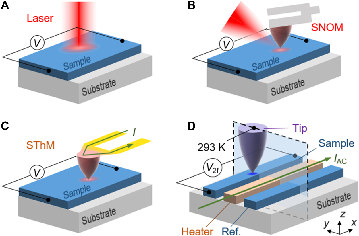
Conceptual drawings of the techniques to map thermoelectric effects. (A) Scanning anomalous Nernst effect microscopy by laser. (B). Scanning near-field optical microscopy (SNOM) (C) Scanning thermal microscopy (SThM). (D) Tip contact method [2].
We have developed a simple method to map the magneto-thermoelectric effects with a high spatial resolution that only requires an AFM with a standard tip and basic instruments such as a lock-in amplifier [2]. Instead of using a built-in heater on the SThM tip, we use a heating wire structured next to the sample wire on a substrate. These wires can be fabricated from a thin film at the same time of the sample fabrication. In conventional SThM, improving spatial resolution is difficult because the typical tip apex radius (rtip ∼ 50–100 nm) is much larger than a standard tip [13, 14]. Our method allows using a standard tip with rtip < 10 nm, which is expected to improve the spatial resolution significantly. The principle of our method is illustrated in Figure 1D. An AC current of the frequency f is applied to the heating wire, leading to a temperature increase of the sample due to Joule heating. The temperature modulation is typically a few K. We bring the AFM tip in contact with the sample surface, which creates a local out-of-plane temperature gradient at the contact point that oscillates at the 2f frequency due to the heat flow from the sample to the tip. When the sample wire exhibits the ANE, a 2f voltage can be detected between both ends, proportional to the magnetization projected onto the wire width axis. It should, however, be noted that an in-plane temperature gradient is also induced, having two order of magnitude smaller than that of out-of-plane temperature gradient, which does not contribute to the signal when we consider the magnetization in-plane. This enables the mapping of the ANE using the contact mode of the AFM. We applied this method to the Weyl ferromagnet Co2MnGa (CMG) [15, 16] for magnetic imaging with a spatial resolution of ∼80 nm [2].
We respectively show the ANE and Seebeck effect (SE) mapping on a Ni80Fe20 (Py) wire and at the Py/Cu junction in Figure 2. While some of the results have already been shown in the supplemental materials of our previous work [2], we demonstrate here that the ANE and SE can be distinguished by examining their magnetic field dependence. Our device consists of 80-nm-thick Py wires fabricated through a lift-off procedure using electron beam evaporation on a SiO2(300 nm)/Si substrate, including 100-nm-thick Cu electrodes and Py/Cu junctions. The widths of the sample and heater are 200 nm and 2 μm, respectively. An edge-to-edge distance of 200 nm separates these two wires. We use an atomic force microscope CoreAFM from Nanosurf [17]. In Figure 2A, we show the AFM topography of the device and the electrical measurement configuration. An alternating current of 17 mA at 1.043 kHz is applied through the heater, and the resulting tip induced signals V2f are mapped during the AFM scanning in contact mode with the loading force of 50 nN using a silicon cantilever (BudgetSensors, Tap190Al-G, spring constant = 48 N/m). The experiment is conducted in atmosphere at room temperature.
FIGURE 2
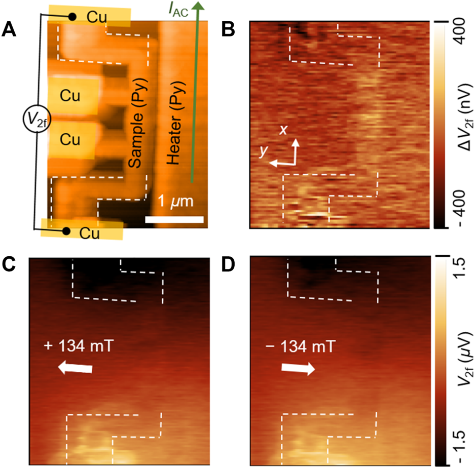
Mapping of the thermoelectric effects of a permalloy (Py: Ni80Fe20) device. (A) Topographic image of the Py device, on which the electrical measurement configuration is indicated. The white dotted lines indicate the position of the sample. (B) The difference between (C) and (D), that eliminate the Seebeck effect and extracts the anomalous Nernst effect of the Py wire. (C), (D) The raw data of V2f mappings with an external magnetic fields of +134 and −134 mT along the wire width direction, respectively.
Results and discussion
Figures 2C, D shows the raw data of V2f mappings acquired under a magnetic field of ±134 mT in the direction of the wire width. The results of the mapping are reproducible and stable over hours. This implies that the system reaches thermal steady state quickly after the tip contact. Significant signals of ±700 nV independent of the magnetic field are observed in the upper and lower parts in Figures 2C, D. The SE can explain these signals at the Py/Cu and Cu/Py junctions. According to the simulation shown later, the temperature change ΔT at the junction due to the tip contact is ∼30 mK. Using Py and Cu Seebeck coefficients of SCu ∼ 1.8 μV/K [18] and SPy ∼ −20 μV/K [19], respectively, the Seebeck voltage is expected to be VSE = (SCu–SPy)·ΔT ∼ 700 nV, which agrees well with experimental values. However, the anisotropic signal in the ANE is barely visible in the magnetic field direction dependence. We can extract the signal which depends on the magnetic field from the difference between Figures 2C, D, as shown in Figure 2B. As a result, every non-magnetic component can be eliminated, and the magnetic components are added up due to their sign change upon magnetization reversal. A signal inside the Py wire is visible that is attributable to the ANE. The magnitude of the ANE signal in Figure 2B is = 120 nV.
This section provides a quantitative discussion of the temperature gradient locally induced by the tip contact. First, we compare the vertical temperature gradient induced by the tip contact method on a CMG device [2] and the laser method on Co2FeAl described in Ref. [3], in which the magnitude of the ANE of these materials have been known. We assume that the locally induced out-of-plane temperature gradient is uniform in a cylindrical region with a bottom surface of A = πrres2, where rres is the spatial resolution [13] (The temperature gradient has a spatial distribution in reality, but using the average value () is convenient to discuss the magnitude). When the magnetization points to the wire width direction, and rres is smaller than the width of the sample, w, the locally induced ANE voltage is given by the following equation:
By substituting the experimental values of , and rres into Eq. 1, we obtain . The results are shown in Table 1. The tip contact method can induce a larger vertical temperature gradient in a much smaller local area than the laser method. However, reducing the sample wire width to ∼1 μm or less in the tip contact method might be necessary to obtain a sufficiently large signal since area A is very small. Measuring samples with a width greater than 10 μm is considered almost impossible.
TABLE 1
| (nV) | (μV/K) | (nm) | w (μm) | (K/μm) | Ref | |
|---|---|---|---|---|---|---|
| Laser (Co2FeAl) | 150 | 0.13 | 5,000 | 80 | 1.2 | [3] |
| Tip contact (Co2MnGa) | 1,200* | 5 | 80 | 0.6 | 7.3 | [2] |
| Tip contact (Py) | 60 | 0.10 | 80 | 0.2 | 6.1 | Figure 2B |
The values in Eq. 1 and estimated temperature gradient for each experiment (*In our experiments on Co2MnGa wires using Si tip (cantilever 190-Al) with a current of 4 mA for the heater, a signal of = 1,200 nV was observed.).
To estimate an unknown magnitude of the ANE , the magnitude of the vertical temperature gradient is required. Here, we attempt to simulate using COMSOL Multiphysics [20]. The heat transfer mechanisms [21] between the tip and sample in contact condition consist of 1) air conduction, 2) water meniscus, 3) solid-solid conduction, and 4) radiation. The contribution of 1) and 2) is known to be significant, while that of 3) is small, and that of 4) is negligible [22]. We introduce the contact thermal conductance Gc and the contact thermal radius rc as phenomenological parameters representing the total effects of (1)–(3), avoiding separating these mechanisms. Our model is shown in Figure 3A, where the tip apex and the sample are thermally connected by a thin disc-shaped region with Gc and rc. The Heat Transfer in Solids interface in COMSOL Multiphysics is used for the simulation. We set a geometry similar to the real CMG device [2], as shown in Figure 3B, which is a cross-section enclosed by dotted lines in Figure 1D. To focus on the ANE, the Cu electrodes are omitted. The temperatures of the substrate boundary and the bottom base of the tip are fixed to 293 K. The thermal conductivities of Si (tip and substrate) and SiO2 are set to 130 W/mK and 1.4 W/mK, respectively. The resistivity of Py is set to 20 μΩ·cm. The disc with the parameters Gc and rc is inserted in between the tip apex and the sample surface. We also set a reference wire without tip contact on the right-hand side of the heater. The applied current to the heater is 4 mA, which results in a temperature increase of 1.3 K from the initial value of 293 K. By putting Gc = 20 μW/K and rex = 30 nm, the simulation gives value of (∼7.2 K/μm: the averaged value in the cylinder) that is locally induced below the tip. On the other hand, there is almost no temperature gradient in the reference wire without tip contact. These parameters (Gc and rc) are reasonable considering that the heat transfer due to 1) and 2) are the main contribution [22], and that rc should be larger than rtip (∼10 nm) but smaller than rres (= 80 nm). Therefore, the experimental results can be well explained by a simulation using appropriate parameters.
FIGURE 3
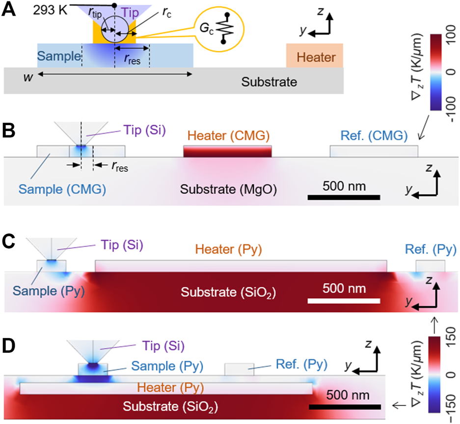
Simulation of locally induced out-of-plane temperature gradient. (A) The heat transport model between the tip and sample. (B), (C) The simulated distribution of the out-of-plane temperature gradient in CMG [2] and Py devices, respectively. (D) Same, but for a device with a heater (Py) embedded beneath the sample.
We estimate the magnitude of the ANE SANE in the Py from the experimental results shown in Figure 2B and the simulation. Interestingly, the reported values of SANE for Py vary significantly between 0.005–2.6 μV/K in the literature [7, 23–27]. Figure 3C shows the spatial distribution of the simulated vertical temperature gradient using the parameters Gc = 20 μW/K, rc = 30 nm. The heater current of 17 mA increases the sample temperature by approximately 3.0 K. Similar to the CMG device, a large vertical temperature gradient appears in the local region under the tip. The magnitude of is ∼6.1 K/μm. Using Eq. 1, SANE in the Py is estimated to be ∼0.10 μV/K. Although this value changes depending on the composition of Ni and Fe, the reported giant value ∼2 μV/K can be the result from underestimation of the temperature gradient.
Our technique enables us to map the ANE even in materials with small SANE. However, the signal can be hard to detect for materials with SANE < 0.10 μV/K (<120 nV). To obtain a more significant signal for a better signal-to-noise ratio, another device geometry has to be considered, such as a device with a heater embedded beneath the sample. Figure 3D shows the simulation result of a device where the heater (Py) is placed under a 50 nm-thick SiO2 layer. An applied current of 17 mA increases the sample temperature by approximately 16 K from the initial temperature. In this geometry, we obtain is ∼33 K/μm, resulting in a five times larger signal than the previous devices. Additionally, Figure 3D indicates that the tip contact induces sizeable local temperature gradients in the sample wire and the insulator below the Py. Therefore, measuring the longitudinal spin Seebeck effect [27] in the same geometry would be possible by replacing Py and SiO2 with a spin Hall material, such as Pt, and a magnetic insulator, respectively.
Conclusion
We demonstrated that inducing a local temperature gradient by tip contact can enable the mapping of thermoelectric effects such as the anomalous Nernst effect, Seebeck effect, and longitudinal spin Seebeck effect with high spatial resolution. The advantage of this technique is that it requires only a conventional atomic force microscope. We have shown that quantitative discussions on the thermoelectric coefficient are possible by introducing phenomenological parameters representing the thermal exchange between the tip and sample. This method enables us to map thermoelectric effects in nanoscale devices and provide information on the uniformity of anomalous Nernst effect and the direction of magnetization at zero external magnetic field, which are the essential information and will play a crucial role for evaluating and optimizing magneto-thermoelectric devices consisting of nanowires. Moreover, this technique can be used for magnetic imaging of materials that exhibit the anomalous Nernst effect. The antiferromagnetic Weyl semimetals Mn3X (X = Sn, Ge) [28] are promising candidates for use in antiferromagnetic spintronics, but the magnetic domain structures have not been clarified yet. Our technique provides magnetic imaging of these materials.
Statements
Data availability statement
The original contributions presented in the study are included in the article/Supplementary Material, further inquiries can be directed to the corresponding author.
Author contributions
HI: Conceptualization (equal); Funding acquisition (supporting); Data curation (equal); Formal analysis (equal); Investigation (lead); Methodology (lead); Visualization (lead); Validation (equal); Writing–original draft (lead); Writing–review and editing (equal). NB: Conceptualization (supporting); Data curation (equal); Formal analysis (equal); Investigation (supporting); Methodology (supporting); Visualization (equal); Writing–original draft (supporting); Writing–review and editing (equal). YO: Conceptualization (equal); Funding acquisition (lead); Project administration (lead); Supervision (lead); Validation (equal); Writing–review and editing (equal). All authors contributed to the article and approved the submitted version.
Funding
This work was partially supported by CREST (Grant No. JPMJCR18T3) from JST, and JSPS KAKENHI (Grant Nos. 19K15431, 19H05629 and 23K04579).
Conflict of interest
The authors declare that the research was conducted in the absence of any commercial or financial relationships that could be construed as a potential conflict of interest.
Publisher’s note
All claims expressed in this article are solely those of the authors and do not necessarily represent those of their affiliated organizations, or those of the publisher, the editors and the reviewers. Any product that may be evaluated in this article, or claim that may be made by its manufacturer, is not guaranteed or endorsed by the publisher.
References
1.
GongXQianRXueHLuWAnZ. Progress of microscopic thermoelectric effects studied by micro- and nano-thermometric techniques. Front Phys (2022) 17:23201. 10.1007/s11467-021-1101-x
2.
BudaiNIsshikiHUesugiRZhuZHigoTNakatsujiSet alHigh-resolution magnetic imaging by mapping the locally induced anomalous Nernst effect using atomic force microscopy. Appl Phys Lett (2023) 122:102401. 10.1063/5.0136613
3.
WeilerMAlthammerMCzeschkaFDHueblHWagnerMSOpelMet alLocal charge and spin currents in magnetothermal landscapes. Phys Rev Lett (2012) 108:106602. 10.1103/physrevlett.108.106602
4.
BartellJMNgaiDHLengZFuchsGD. Towards a table-top microscope for nanoscale magnetic imaging using picosecond thermal gradients. Nat Commun (2015) 6:8460. 10.1038/ncomms9460
5.
MartensUHuebnerTUlrichsHReimerOKuschelTTammingRRet alAnomalous Nernst effect and three-dimensional temperature gradients in magnetic tunnel junctions. Commun Phys (2018) 1:65. 10.1038/s42005-018-0063-y
6.
JohnsonFKimákJZemenJŠobáňZSchmoranzerováEGodinhoJet alIdentifying the octupole antiferromagnetic domain orientation in Mn 3 NiN by scanning anomalous Nernst effect microscopy. Appl Phys Lett (2022) 120:232402. 10.1063/5.0091257
7.
Von BierenABrandlFGrundlerDAnsermetJP. Space- and time-resolved Seebeck and Nernst voltages in laser-heated permalloy/gold microstructures. Appl Phys Lett (2013) 102:052408. 10.1063/1.4789974
8.
PfitznerEHuXSchumacherHWHoehlAVenkateshvaranDCubukcuMet alNear-field magneto-caloritronic nanoscopy on ferromagnetic nanostructures. AIP Adv (2018) 8. 10.1063/1.5054382
9.
JandaTGodinhoJOstatnickyTPfitznerEUlrichGHoehlAet alMagneto-seebeck microscopy of domain switching in collinear antiferromagnet CuMnAs. Phys Rev Mater (2020) 4:094413. 10.1103/physrevmaterials.4.094413
10.
ZhangCBartellJMKarschJCGrayIFuchsGD. Nanoscale magnetization and current imaging using time-resolved scanning-probe magnetothermal microscopy. Nano Lett (2021) 21:4966–72. 10.1021/acs.nanolett.1c00704
11.
MajumdarA. Scanning thermal microscopy. Annu Rev Mater Sci (1999) 29:505–85. 10.1146/annurev.matsci.29.1.505
12.
ZhangYZhuWHuiFLanzaMBorca-TasciucTMuñoz RojoM. A review on principles and applications of scanning thermal microscopy (SThM). Adv Funct Mater (2020) 30:1900892. 10.1002/adfm.201900892
13.
PuyooEGraubySRampnouxJMRouvìreEDilhaireS. Thermal exchange radius measurement: Application to nanowire thermal imaging. Rev Sci Instrum (2010) 81:073701. 10.1063/1.3455214
14.
KimKJeongWLeeWReddyP. Ultra-high vacuum scanning thermal microscopy for nanometer resolution quantitative thermometry. ACS Nano (2012) 6:4248–57. 10.1021/nn300774n
15.
SakaiAMizutaYPNugrohoAASihombingRKoretsuneTSuzukiMTet alGiant anomalous Nernst effect and quantum-critical scaling in a ferromagnetic semimetal. Nat Phys (2018) 14:1119–24. 10.1038/s41567-018-0225-6
16.
ZhuZHigoTNakatsujiSOtaniY. Magnetic and transport properties of amorphous, B 2 and L 2 1 Co 2 MnGa thin films. AIP Adv (2020) 10:085020. 10.1063/5.0018640
17.
BippesCFrederixPWertenPYablonD. CoreAFM: Research-Grade AFM platform with application modularity. Micros Today (2017) 25:20–5. 10.1017/s1551929517000992
18.
KendallNCKendallP. The absolute scale of thermoelectric power at high temperature. Proc Phys Soc (1958) 72:898–901. 10.1088/0370-1328/72/5/429
19.
UchidaKTakahashiSHariiKIedaJKoshibaeWAndoKet alObservation of the spin Seebeck effect. Nature (2008) 455:778–81. 10.1038/nature07321
20.
COMSOL. Multiphysics® v. 6.1 Www.Comsol.Com. Stockholm, Sweden: COMSOL AB (2022).
21.
ShiLMajumdarA. Thermal transport mechanisms at nanoscale point contacts. J Heat Transfer (2002) 124:329–37. 10.1115/1.1447939
22.
LefèvreSVolzSChapuisPO. Nanoscale heat transfer at contact between a hot tip and a substrate. Int J Heat Mass Transf (2006) 49:251–8. 10.1016/j.ijheatmasstransfer.2005.07.010
23.
SlachterABakkerFLAdamJ-Pvan WeesBJ. Thermally driven spin injection from a ferromagnet into a non-magnetic metal. Nat Phys (2010) 6:879–82. 10.1038/nphys1767
24.
HolandaJAlves SantosOCunhaROMendesJBSRodríguez-SuárezRLAzevedoAet alLongitudinal spin Seebeck effect in permalloy separated from the anomalous Nernst effect: Theory and experiment. Phys Rev B (2017) 95:214421. 10.1103/physrevb.95.214421
25.
ChuangTCSuPLWuPHHuangSY. Enhancement of the anomalous Nernst effect in ferromagnetic thin films. Phys Rev B (2017) 96:174406. 10.1103/physrevb.96.174406
26.
BennetRKHojemAZinkBL. Temperature dependence of the anomalous Nernst coefficient for Ni80Fe20determined with metallic nonlocal spin valves. AIP Adv (2020) 10:065127. 10.1063/5.0006599
27.
IsshikiHZhuZMizunoHUesugiRHigoTNakatsujiSet alDetermination of spin Hall angle in the Weyl ferromagnet Co2MnGa by taking into account the thermoelectric contributions. Phys Rev Mater (2022) 6:084411. 10.1103/physrevmaterials.6.084411
28.
NakatsujiSAritaR. Topological magnets: Functions based on berry phase and multipoles. Annu Rev Condens Matter Phys (2022) 13:119–42. 10.1146/annurev-conmatphys-031620-103859
Summary
Keywords
atomic force microscopy, anomalous Nernst effect, spin caloritronics, magneto-thermoelectric effects, magnetic imaging
Citation
Isshiki H, Budai N and Otani Y (2023) Magneto-thermoelectric effects mapping using tip-induced temperature gradient in atomic force microscopy. Front. Phys. 11:1205556. doi: 10.3389/fphy.2023.1205556
Received
14 April 2023
Accepted
26 June 2023
Published
24 July 2023
Volume
11 - 2023
Edited by
Xiaotian Wang, Southwest University, China
Reviewed by
Jianbao Zhao, Canadian Light Source, Canada
Na Lei, Beihang University, China
Updates
Copyright
© 2023 Isshiki, Budai and Otani.
This is an open-access article distributed under the terms of the Creative Commons Attribution License (CC BY). The use, distribution or reproduction in other forums is permitted, provided the original author(s) and the copyright owner(s) are credited and that the original publication in this journal is cited, in accordance with accepted academic practice. No use, distribution or reproduction is permitted which does not comply with these terms.
*Correspondence: YoshiChika Otani, yotani@issp.u-tokyo.ac.jp
Disclaimer
All claims expressed in this article are solely those of the authors and do not necessarily represent those of their affiliated organizations, or those of the publisher, the editors and the reviewers. Any product that may be evaluated in this article or claim that may be made by its manufacturer is not guaranteed or endorsed by the publisher.