 Ilaria Fratelli1,2*
 Lorenzo Maserati1,3
 Laura Basiricò1,2
 Alessandro Galeazzi1Bianca Passarella3
 Andrea Ciavatti1,2Mario Caironi3
 Beatrice Fraboni1,2
- 1Department of Physics and Astronomy, University of Bologna, Bologna, Italy
- 2National Institute of Nuclear Physics (INFN), Section of Bologna, Bologna, Italy
- 3Center for Nano Science and Technology, Istituto Italiano di Tecnologia, Milan, Italy
X-ray detection for personal dosimetry requires sensitive, stable and non-toxic materials. At the same time, scalability onto large-area and flexible substrates is emerging as a desirable property. To satisfy these requirements, novel materials to be employed as the active layer of direct X-ray detectors are needed. In this search for easy-processability, large area, efficient and non-toxic materials for direct X-ray detection, we assess the performance of a layered metal-organic chalcogenide [AgSePh]∞, recently proposed as representative of a novel excitonic semiconductors platform. Here we demonstrate that [AgSePh]∞ can be successfully applied as direct ionizing radiation detecting layer, reaching sensitivities up to (180 ± 10) μC Gy−1 cm−2 and competitive limit of detection down to (100 ± 30) nGy s−1. Moreover, it offers good stability and reproducibility of detection after 100 Gy of irradiation and upon bending to a curvature radius of 5 mm.
1 Introduction
The research of novel materials able to detect high-energy radiation is a long-lasting topic due to its impact on many diverse fields, spanning from astrophysics to health diagnostic, and security screening. In the last decade, new quests such as scalability onto large and flexible surfaces, low production cost and low-power consumption are emerging. Moreover, additional properties, such as low toxicity, are highly desirable in specific applications such as personal dosimetry during radiation medical treatments or in radiation harsh environments.
For these reasons, the scientific community has recently explored novel materials, and the use of thin films instead of bulky and rigid single crystals as active layers has been put forward [1]. Among inorganic semiconductors, amorphous selenium (a-Se) and polycrystalline Cadmium Zinc Telluride (poly-CZT) represent the benchmark for the development of large-area ionizing radiation detectors [2]. In the last few years, the new materials class of metal halide perovskites (MHP) has been deeply investigated to harness their exceptional optoelectronic properties [14]. MHP offer several advantages such as the high attenuation fraction and excellent transport properties (i.e., high mobility-lifetime product µτ) which lead to outstanding detecting efficiency [1,3–6]. They can be deposited from solution by low-cost fabrication techniques, compatible with flexible polymeric substrates and easy scalable onto large and curved surfaces [7,8]. The main issue related to MHP is the presence of water-soluble lead, which raises concerns related to their use as personal dosimeters. Besides, the fabrication processes of these materials use highly-toxic solvents not compatible with environmental sustainability. To tackle these issues, MHPs with alternative elemental compositions and different fabrication procedures are under study. For instance, green solvents are being tested and lead-free compounds such as MA3Bi2I9 [9,10], Cs2TeI6 [11], Cs2AgBiBr6 [65] are emerging as promising X-ray detection candidates. Nevertheless, devices fabricated with these materials are based on rare elements (e.g., Bi, Te) and present several stability issues under operating conditions: environmental factors, such as humidity, oxygen, temperature, and light, significantly affect material’s stability by inducing phase transitions or segregation, crystal decomposition and erratic current-voltage characteristics. Finally, ion migration is a well-known but still unsolved problem related to this material platform that induces dark current drifts during prolonged biasing [12,13]. A possible alternative toward lead-free low toxic detectors is the employment of organic semiconducting materials as active layers. This approach has already demonstrated good results for different types of radiation (e.g., X-rays [14–20], protons [21,22], neutrons [23]). However, in organic semiconductors the ionizing radiation absorption rate is very poor due to the low-Z of the constituents, which limits the active layer stopping power and ultimately, the detectors’ quantum efficiency.
In the last few years, many studies have shed a spotlight on the peculiar excitonic and optoelectronic properties of self-assembled hybrid quantum wells materials (i.e., highly confined layered materials). Layered MHPs are the most studied among low dimensional hybrid materials for the detection of high energy radiation [24–26,73] because of their high attenuation fraction and potentially high charge carrier mobilities. Despite the excellent performances already reported in literature for this class of materials, the intrinsic instability of the ionic lattice and the presence of toxic elements urged the search for alternative materials. Among other low dimensional hybrids, the covalently bound coordination polymer silver benzeneselenolate [AgSePh]∞ [27–33] has been recently re-discovered as a direct bandgap semiconductor with good optoelectronic performances. This compound is part of a new material class of 2D quantum confined metal-organic chalcogenides materials (MOCs) that offer a simple fabrication via wet chemistry and whose light absorption and emission can be chemically tuned thanks to their peculiar 2D excitonic properties [29,33,34]. These materials are air-stable and do not contain potentially hazardous metals. In 2021, the MOCs strong absorption coefficient and good electrical transport properties have been leveraged to demonstrate the application of [AgSePh]∞ in near-UV photo-detection [27]. Here, further exploring the light matter interaction in the MOC material class, we investigate the response of [AgSePh]∞ in the high energy photon range (i.e. 40 kVp) implementing a new X-ray detector able to overcome many of the limits imposed by the present technologies.
2 Results and discussion
In Figure 1A the sketch of the co-planar X-ray photodetector based on [AgSePh]∞ is illustrated. The device was fabricated on a flexible 125 µm thick PEN (poliyethylene naphtalate) substrate. The gold charge-collecting electrodes were thermally evaporated onto the plastic substrate. The active layer was made by [AgSePh]∞ deposited following the 3-steps procedure described in a previous work [28]. Briefly, a silver thin-film (200 nm thick) was thermally evaporated onto the pre-patterned devices; subsequently, the silver was oxidized by O2 plasma treatment and it underwent chemical transformation into the final product upon exposure to benzeneselenol vapors at 90°C in an inert atmosphere (for more details see Materials and Methods section). The characterization of the chemical composition and the optoelectronic properties of the final [AgSePh]∞ film has been already reported in literature [28]. The optical image of the pixel area (1 mm × 1 mm, channel lengths L = 5 µm or L = 40 µm) and the atomic force microscopy (AFM) map reported in Figure 1B show the nanocrystalline morphology of the deposited film. The tested active layers present a thickness of 2 µm and nanocrystals lateral sizes is about 300 nm. Figure 1B shows the good uniformity and high film coverage over the entire area of the pixel. The fabrication procedure took place at low temperature (T < 100°C), compatible with polymeric substrates, leading to the realization of flexible devices (see Figure 1C). A typical current-voltage IV) curve of the device in dark conditions is reported in Figure 1D. The lack of hysteresis and the electrical dark conductivity of (344 ± 5) pS cm−1 [27] are comparable to what previously reported in literature for similar devices fabricated on PEN substrate. Here the electrical conductivity has been calculated considering the geometrical dimensions of the device (channel length L = 40 μm, width W = 23 mm, active layer thickness = 2 µm) and the linear fit of the IV curve reported in Figure 1D and plotted in linear scale.
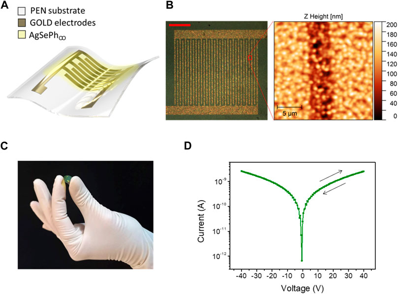
FIGURE 1. X-Ray detectors based on [AgSePh]∞ nanocrystalline films. (A) Sketch of the detector architecture. The [AgSePh]∞ is synthesized on the top of two planar interdigitated gold electrodes thermally evaporated onto a 125 µm-thick PEN foil. (B) Optical image of the pixel area (left, scale bar 250 µm) and AFM image of the nanocrystalline film on the device conductive channel (right). (C) Picture of the flexible device. (D) Current-voltage (IV) curve of the photoconductor in the dark condition (channel length L = 40 μm, width W = 23 mm). The arrows indicate the forward and reverse sweeps.
Thanks to the presence of high-Z elements as silver and selenium, [AgSePh]∞ presents an X-ray stopping power much higher than silicon and organic layers, as it is reported in Figure 2A. For a 1 µm thick active layer of [AgSePh]∞ the attenuated fraction of 15.2 keV photons (i.e., the energy mean value of the radiation spectrum produced by a W-target X-ray tube biased at 40 kVp) is 0.9%, a much higher value than for organic semiconductors (e.g., TIPS-pentacene, 0.01%) and slightly lower than for standard inorganic semiconducting materials (e.g., CZT 3%, CdTe 2%, Se 4%) and hybrid perovskites (2%–3%). This feature is very promising towards the development of efficient X-ray dosimeters to be employed in the medical field, since it provides high attenuation of high energy radiation keeping the low toxicity related to the absence of lead.
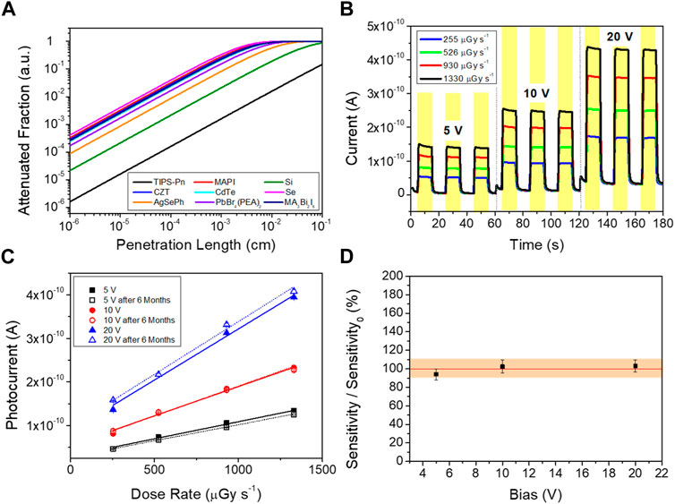
FIGURE 2. X-ray detector characterization. (A) Simulated attenuated fraction of different materials at 15.2 keV photons (mean photon energy in the here employed irradiation conditions: X-rays produced by a Tungsten-target X-ray tube kept at 40 kVp) as a function of the layer thicknesses. (B) Dynamic photocurrent response induced by four different dose rates [255–1,330] mGy s−1 keeping the sample biased in three different conditions (5, 10, 20 V). The same irradiation cycle (10 s ON/10s OFF) has been repeated for three times to test the repeatability of the detecting response. The yellow shadow indicates the period of X-rays ON. (C) Photocurrent induced by different dose rates reported for the three polarization conditions. These data are reported for the sample as fabricated (solid symbols) and after 6 months stored in ambient conditions (open symbols). The sensitivity is calculated as the slope of the fitting curves. (D) Variation of the sensitivity reported for the three bias voltages.
We characterized the devices under X-rays produced by a W-target tube kept at 40 kVp and varying the dose rate by changing the current in the range [100–500] µA. Figure 2B shows the dynamic response of the detector for three different bias conditions (i.e. 5, 10, 20 V). The sample was irradiated by subsequent irradiation cycles (10 s ON, 10 s OFF) at four different dose rates (255, 526, 930, 1,330 μGy s−1). For each dose rate, three consecutive identical irradiation cycles were performed to test the repeatability of the detector response. We calculated the photocurrent as the variation of the current flowing in the device channel when the X-rays are turned ON (
The maximum measured value of sensitivity per unit area is S = (180 ± 10) μC Gy−1 cm−2 (when an electric field of 5,000 V m−1 is applied and a pixel area of 1 mm2 is considered). Considering this operation conditions, this sensitivity value is comparable with the ones reported for full-organic and hybrid perovskite thin film-based X-ray detectors and higher than the sensitivity of a-Se and poly-CZT, which represent the inorganic benchmarks for large area ionizing radiation detection [1,20,35].
Figures 2C, D show the detector response as fabricated and after 6 months stored in dark ambient conditions (i.e., air, room temperature). The samples do not present any degradation due to the aging and the detector performance remains constant with a sensitivity variation within 10% with respect to the pristine device values. The excellent stability represents a further great advantage of this sensing material platform. Other materials such as MHPs present comparable X-ray efficiency but poorer stability if not encapsulated and stored in ambient conditions which limits their employment in real applications. For MHPs single crystals (SC), the longest ageing studies reported so far are of about 6 months by Kovalenko et al. (non-incapsulated MAPbI3 SC, efficiency degradation 12%) [36], and 2 months by Liu et al. (MA3Bi2I9 SC, photocurrent degradation 9.2%) [37] and by Wei et al. (MAPbBr3 SC) [38]. For MHP polycrystalline films Zhao et al. reported a MAPbI3 membrane which showed an unchanged sensitivity after 6 months of storage in nitrogen [39] and Glushkova et al. demonstrated stability after 9 months ageing of a MAPbI3 film encapsulated with PDMS (Polydimethylsiloxane) [8]. Only the last year, Fraboni et al. reported a record stability (97% after 630 days) for two different perovskite films (i.e., MAPbI3 and FAxMA1–xPbI3) deposited using starch as templating agent [40].
The proposed detector is demonstrated to be radiation tolerant up to a tested total dose of 100 Gy air kerma. As it is shown in Figure 3A, the variation of the photocurrent response remains constant (within 5%) up to this total irradiation, which corresponds, for instance, to the typical value delivered for 6.7 million of full-mouth dental radiographies [41]. The Limit of Detection (LoD) represents the lowest detectable dose that a device can detect. Under the assumption that noise is dominated by dark current shot noise, the LoD value can be defined [42] as the dose of radiation that induces a signal three times higher than the electrical noise (i.e., root mean square of the dark current). We calculated the LoD using the following equation:
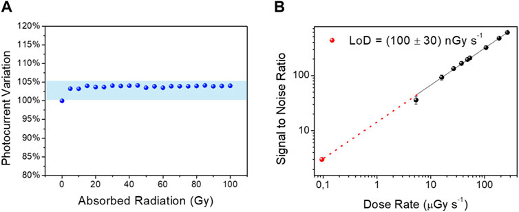
FIGURE 3. Radiation hardness and Limit of Detection (LoD). (A) Radiation hardness test. The sample has been irradiated until a total absorbed radiation dose of 100 Gy. The photocurrent induced in the device has been monitored after each 5 Gy and its variation respect the pristine is reported. (B) Signal to Noise Ratio reported as a function of the Dose Rate. The signal is the photocurrent induced by each dose rate and the noise is the Root Mean Square of the dark current. The sample has been biased at 20 V. The red symbol is the lowest detectable dose LoD = (300 ± 10) nGy s−1.
The LoD is (100 ± 30) nGy s−1 and it is reported in Figure 3B for a sample biased at 20 V.
In Figure 4 the LoD value estimated by these samples is compared with the state of the art for detectors based on organic semiconductors [15,43–48] and perovskites active layers in the form of single crystal [3,4,37,38,49–62] or polycrystalline films [9,10,63–72]. Moreover, in the graph it is highlighted the performances achieved by lead-free materials. The [AgSePh]∞-based detector offers a limit of detection lower than most of the lead-free detectors reported in Figure 4. This result makes this material very promising for possible employment in the medical field where conformable and portable detectors based on low toxic materials able to detect low doses of radiation are required. For instance, typical dose rate used for diagnostics is about 5 μGy s−1 [73].
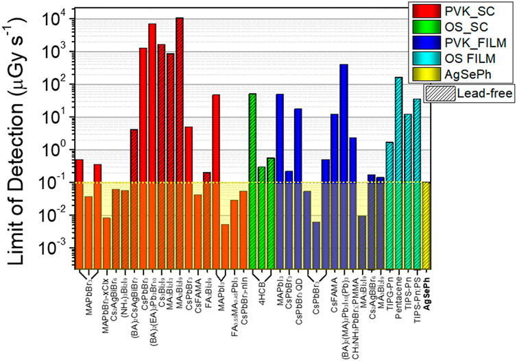
FIGURE 4. Limit of Detection–State of the Art. Limit of Detection (LoD) reported in literature for metal halide perovskite single crystals (red) [3,4,37,38,49–62], organic semiconductor single crystals (green) [43–45], perovskite films (blue) [9,10,63–72], organic semiconductor films (blue light) [15,46–48] and [AgSePh]∞ nanocrystalline films (yellow) X-ray detectors. The black shadows indicate the lead-free materials.
The mechanical flexibility tests of the devices fabricated on PEN substrates are shown in Figure 5. The samples were mounted in the stretching tool depicted in Figure 5A and they were bent gradually at different curvature radii (CR), starting from the flat condition to CR = 0.17 cm (see Figure 5B). The sample was irradiated at each CR and the X-ray induced photocurrent has been measured. In Figure 5C the variation of the photocurrent with respect to that achieved in the flat condition is reported as a function of the curvature radius and it results within 25% for CR > 0.5 cm. At smaller curvature radii, the photocurrent gradually decreases and at the lowest curvature radius CR = 0.17 cm it is about 30% of the initial value. After this fatigue test, the sample was irradiated again in the flat condition and the collected photocurrent totally recovered, suggesting that the photocurrent decrease is due to reversible mechanical factors other than to a permanent damage of the active layer.
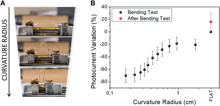
FIGURE 5. Flexibility tests. (A) Photographs of the sample bent at different curvature radius starting from the flat condition until CR = 0.17 cm. (B) Photocurrent variation percentages versus Curvature radius.
3 Materials and methods
3.1 Devices fabrication
Metal contact patterning on substrates was performed by thermal evaporation of Cr/Au evaporation (1.5 nm and 35 nm, respectively) on PEN substrates after maskless optical lithography (SU8 photoresist) to pattern interdigitated electrodes. The electrodes were designed to implement a device channel length of 5 or 40 μm with a fixed channel width of 30 mm.
The [AgSePh]∞ nano-crystal (NC) film synthesis started with 200 nm-thick silver films thermally evaporated on PEN substrates with pre-patterned metal contacts. The samples were then exposed to O2 plasma at a pressure of 0.4 mbar with a nominal power of 10 W for 1 min to form AgO. A Diener Electronic Femto Plasma asher was used. Subsequently, the silver oxide films were exposed to a chemical vapor process. Benzeneselenol (97%, Sigma Aldrich) was introduced into a nitrogen glove box in a Teflon-lined 22 mL vial next to the AgO covered substrate. The sealed vial was transferred in a pre-heated oven at 90°C. The reaction yielded [AgSePh]∞ after 4 h. All the samples were rinsed in acetone and then with isopropyl alcohol to remove the unreacted organo-chalcogen reagent and N2 dried in a box, overnight.
3.2 X-ray detection experiment
The samples have been tested as X-ray detectors by monitoring the current flowing in the channel of the device under irradiation cycles. The samples have been electrically connected to a Source Meter Unit (Keithley 2614B) and they have been closed in a shielded metallic box during the measurements to screen them from electromagnetic noise and visible light. During the irradiation tests, the samples have been continuously biased, and the variation of the current has been monitored. As X-ray source, we employed a W-target X-Ray tube kept at 40 kVp (15.2 keV mean energy of the spectrum) and with an anodic current spanning in the range [100–500] µA. The samples have been irradiated by subsequent irradiation cycles (10 s X-ray ON//10s X-ray OFF) at different dose rates (from 6 μGy s−1 up to 1,330 μGy s−1). The photocurrent induced has been calculated as the difference between the current flowing in the sample when the X-Rays are turned ON and the dark current.
3.3 Electrical characterization
Electrical characterization has been performed with a dual channel Keithley 2614B SourceMeter, using triaxial cables (that ensure low noise down to 100 fA and low parasitic capacitance) and custom made Labview software. All measurements are carried out keeping the device in dark in a metal Faraday cage to reduce electrical noise and avoid light-induced photogeneration in the organic semiconductor.
3.4 AFM measurements
AFM measurements: AFM measurements are performed on a Park NX10 system using PPP-NCHR tips (Nanosensors) in non-contact mode and applying adaptive scan-rate to slow down scan speed at crystallite borders. The area scan is 20 μm × 20 µm.
3.5 Bending tests
Mechanical tests have been performed by mounting the samples on a custom stretcher tool. The samples have been kept at different curvature radius (CR = [flat–0.17] cm) while they have been electrically characterized in dark condition and under X-rays.
4 Conclusion
We reported the fabrication and testing of a novel direct X-ray detector based on a quantum confined metal-organic chalcogenide. A nanocrystalline film of silver benzene selenolate [AgSePh]∞ was synthesized on metal contacts and used as the active layer in a planar photodetector configuration. The MOC offers several advantages with respect other materials candidate for direct X-ray detection: 1) it is processable at low temperature onto polymeric and flexible substrate by easily scalable fabrication techniques; 2) it presents a high attenuation fraction thanks to the high-Z elements, avoiding the presence of lead and providing low toxicity level due to the presence of low-toxic elements, highly desirable in medical field; 3) it is shows good shelf-life stability, with only a 10% of X-ray response degradation after 6 months of storage in ambient conditions. We leveraged these unique properties to demonstrate high MOC X-ray detector performances: sensitivity = (180 ± 10) μC Gy−1 cm−2, LoD = (100 ± 30) nGy s−1, radiation hardness up to 100 Gy, and good mechanical stability down to a curvature radius of 5 mm. Our results suggest a new application for an underexplored class of sustainable low-dimensional hybrid material that provides exceptional optoelectronic properties, excellent to be exploited for flexible and large-area X-Ray direct detectors.
Data availability statement
The original contributions presented in the study are included in the article/supplementary material, further inquiries can be directed to the corresponding author.
Author contributions
IF: Conceptualization, Investigation, Writing–original draft, Writing–review and editing. LM: Conceptualization, Investigation, Writing–review and editing. LB: Conceptualization, Investigation, Writing–review and editing. AG: Investigation, Writing–review and editing. BP: Investigation, Writing–review and editing. AC: Conceptualization, Software, Writing–review and editing. MC: Conceptualization, Supervision, Writing–review and editing. BF: Supervision, Writing–review and editing.
Funding
The authors declare that no financial support was received for the research, authorship, and/or publication of this article.
Conflict of interest
The authors declare that the research was conducted in the absence of any commercial or financial relationships that could be construed as a potential conflict of interest.
The authors declared that they were an editorial board member of Frontiers, at the time of submission. This had no impact on the peer review process and the final decision.
Publisher’s note
All claims expressed in this article are solely those of the authors and do not necessarily represent those of their affiliated organizations, or those of the publisher, the editors and the reviewers. Any product that may be evaluated in this article, or claim that may be made by its manufacturer, is not guaranteed or endorsed by the publisher.
References
1. Basiricò L, Ciavatti A, Fraboni B. Solution-Grown organic and perovskite X-ray detectors: a new paradigm for the direct detection of ionizing radiation. Adv Mater Technol (2020) 6:2000475. doi:10.1002/admt.202000475
2. Kasap S, Frey JB, Belev G, Tousignant O, Mani H, Greenspan J, et al. Amorphous and polycrystalline photoconductors for direct conversion flat panel x-ray image sensors. Sensors (2011) 11:5112–57. doi:10.3390/s110505112
3. Wei H, DeSantis D, Wei W, Deng Y, Guo D, Savenije TJ, et al. Dopant compensation in alloyed CH3NH3PbBr3−xClx perovskite single crystals for gamma-ray spectroscopy. Nat Mater (2017) 16(8):826–33. doi:10.1038/nmat4927
4. Liu Y, Zhang Y, Zhu X, Feng J, Spanopoulos I, Ke W, et al. Triple-cation and mixed-halide perovskite single crystal for high-performance X-ray imaging. Adv Mater (2021) 33(8):e2006010–10. doi:10.1002/adma.202006010
5. Basiricò L, Senanayak SP, Ciavatti A, Abdi-Jalebi M, Fraboni B, Sirringhaus H. Detection of X-rays by solution-processed cesium-containing mixed triple cation perovskite thin films. Adv Funct Mater (2019) 29(34):1–9. doi:10.1002/adfm.201902346
6. Yakunin S, Sytnyk M, Kriegner D, Shrestha S, Richter M, Matt GJ, et al. Detection of X-ray photons by solution-processed lead halide perovskites. Nat Photon (2015) 9(7):444–9. doi:10.1038/nphoton.2015.82
7. Demchyshyn S, Verdi M, Basiricò L, Ciavatti A, Hailegnaw B, Cavalcoli D, et al. Designing ultraflexible perovskite X-ray detectors through interface engineering. Adv Sci (2020) 7:2002586. doi:10.1002/advs.202002586
8. Glushkova A, Andričević P, Smajda R, Náfrádi B, Kollár M, Djokić V, et al. Ultrasensitive 3D aerosol-jet-printed perovskite X-ray photodetector. ACS Nano (2021) 15(3):4077–84. doi:10.1021/acsnano.0c07993
9. Dong S, Xin D, Zhang M, Tie S, Cai B, Ma Q, et al. Green solvent blade-coated MA3Bi2I9 for direct-conversion X-ray detectors. J Mater Chem C (2022) 10(16):6236–42. doi:10.1039/d2tc00522k
10. Tie S, Zhao W, Xin D, Zhang M, Long J, Chen Q, et al. Robust fabrication of hybrid lead-free perovskite pellets for stable X-ray detectors with low detection limit. Adv Mater (2020) 32(31):e2001981. doi:10.1002/adma.202001981
11. Guo J, Xu Y, Yang W, Xiao B, Sun Q, Zhang X, et al. High-stability flexible X - ray detectors based on lead-free halide perovskite Cs2 TeI6 films. ACS Appl Mater Inter. 2021;13. 23928–35. doi:10.1021/acsami.1c04252
12. Aktas E, Rajamanickam N, Pascual J, Hu S, Aldamasy MH, Di Girolamo D, et al. Challenges and strategies toward long-term stability of lead-free tin-based perovskite solar cells. Commun Mater (2022) 3(1):104–14. doi:10.1038/s43246-022-00327-2
13. Wu Y, Feng J, Yang Z, Liu Y, Liu S. Halide perovskite: a promising candidate for next-generation X-ray detectors. Adv Sci (2023) 10(1):e2205536–48. doi:10.1002/advs.202205536
14. Basiricò L, Ciavatti A, Cramer T, Cosseddu P, Bonfiglio A, Fraboni B. Direct X-ray photoconversion in flexible organic thin film devices operated below 1 V. Nat Commun (2016) 7(1):13063. doi:10.1038/ncomms13063
15. Temiño I, Basiricò L, Fratelli I, Tamayo A, Ciavatti A, Mas-Torrent M, et al. Morphology and mobility as tools to control and unprecedentedly enhance X-ray sensitivity in organic thin-films. Nat Commun (2020) 11(1):2136–10. doi:10.1038/s41467-020-15974-7
16. Thirimanne HM, Jayawardena KDGI, Parnell AJ, Bandara RMI, Karalasingam A, Pani S, et al. High sensitivity organic inorganic hybrid X-ray detectors with direct transduction and broadband response. Nat Commun (2018) 9(1):2926. doi:10.1038/s41467-018-05301-6
17. Large MJ, Posar JA, Mozer AJ, Nattestad A, Alnaghy S, Carolan M, et al. Flexible polymer X - ray detectors with non-fullerene acceptors for enhanced stability: toward printable tissue equivalent devices for medical applications. ACS Appl Mater Inter (2021) 13(48):57703–12. doi:10.1021/acsami.1c16914
18. Nanayakkara MPA, Masteghin MG, Basiricò L, Fratelli I, Ciavatti A, Kilbride RC, et al. Molecular weight tuning of organic semiconductors for curved organic – inorganic hybrid X-ray detectors. Adv Sci (Weinh). 9. 2021:1–15. doi:10.1002/advs.202101746
19. Fratelli I, Basiricò L, Ciavatti A, Lamport ZA, Anthony JE, Kymissis I, et al. Trap states ruling photoconductive gain in tissue- equivalent, printed organic X-ray detectors. Adv Mater Technol (2022) 8:2200769. doi:10.1002/admt.202200769
20. Tamayo A, Fratelli I, Ciavatti A, Martínez-Domingo C, Branchini P, Colantoni E, et al. X-Ray detectors with ultrahigh sensitivity employing high performance transistors based on a fully organic small molecule semiconductor/polymer blend active layer. Adv Electron Mater (2022) 8:2200293. doi:10.1002/aelm.202200293
21. Fratelli I, Ciavatti A, Zanazzi E, Basiricò L, Chiari M, Fabbri L, et al. Direct detection of 5-MeV protons by flexible organic thin-film devices. Sci Adv (2021) 7(16):eabf4462. doi:10.1126/sciadv.abf4462
22. Calvi S, Basiricò L, Carturan SM, Fratelli I, Valletta A, Aloisio A, et al. Flexible fully organic indirect detector for megaelectronvolts proton beams. Npj Flex Electron (2023) 7:5–11. doi:10.1038/s41528-022-00229-w
23. Chatzispyroglou P, Keddie JL, Sellin PJ. Boron-loaded polymeric sensor for the direct detection of thermal neutrons. ACS Appl Mater Inter (2020) 12(29):33050–7. doi:10.1021/acsami.0c09998
24. He X, Xia M, Wu H, Du X, Song Z, Zhao S, et al. Quasi-2D perovskite thick film for X-ray detection with low detection limit. Adv Funct Mater (2022) 32(7):2109458. doi:10.1002/adfm.202109458
25. Lédée F, Ciavatti A, Verdi M, Basiricò L, Fraboni B, Lédée F, et al. Ultra-stable and robust response to X-rays in 2D layered perovskite micro-crystalline films directly deposited on flexible substrate. Adv Opt Mater (2022) 10(1):2101145. doi:10.1002/adom.202101145
26. Basiricò L, Fratelli I, Verdi M, Ciavatti A, Barba L, Cesarini O, et al. Mixed 3D – 2D perovskite flexible films for the direct detection of 5 MeV protons. Adv Mater (2022) 2204815:1–8. doi:10.1002/advs.202204815
27. Maserati L, Prato M, Pecorario S, Passarella B, Perinot A, Thomas AA, et al. Photo-electrical properties of 2D quantum confined metal-organic chalcogenide nanocrystal films. Nanoscale (2021) 13(1):233–41. doi:10.1039/d0nr07409h
28. Maserati L, Pecorario S, Prato M, Caironi M. Understanding the synthetic pathway to large-area, high-quality [AgSePh]∞Nanocrystal films. J Phys Chem C (2020) 124(41):22845–52. doi:10.1021/acs.jpcc.0c07330
29. Kastl C, Schwartzberg AM, Maserati L. Picoseconds-limited exciton recombination in metal-organic chalcogenides hybrid quantum wells. ACS Nano (2022) 16(3):3715–22. doi:10.1021/acsnano.1c07281
30. Paritmongkol W, Lee WS, Shcherbakov-Wu W, Ha SK, Sakurada T, Oh SJ, et al. Morphological control of 2D hybrid organic-inorganic semiconductor AgSePh. ACS Nano (2022) 16(2):2054–65. doi:10.1021/acsnano.1c07498
31. Paritmongkol W, Sakurada T, Lee WS, Wan R, Müller P, Tisdale WA. Size and quality enhancement of 2D semiconducting metal-organic chalcogenolates by amine addition. J Am Chem Soc (2021) 143(48):20256–63. doi:10.1021/jacs.1c09106
32. Schumann H, Freckmann DMM, Dechert S. The molecular structure of tris (trimethylsilylmethyl) samarium, -erbium, -ytterbium, and -lutetium. John Wiley Sons, Ltd (2002)(628) 2422–6. doi:10.1002/1521-3749(200211)628:11<2422::AID-ZAAC2422>3.0.CO;2-B
33. Yao K, Collins MS, Nell KM, Barnard ES, Borys NJ, Kuykendall T, et al. Strongly quantum-confined blue-emitting excitons in chemically configurable multiquantum wells. ACS Nano (2021) 15(3):4085–92. doi:10.1021/acsnano.0c08096
34. Kastl C, Bonfà P, Maserati L. Anharmonic exciton-phonon coupling in metal-organic chalcogenides hybrid quantum wells. Adv Opt Mater (2023) 11(7). doi:10.1002/adom.202202213
35. Kabir MZ, Kasap S. Photoconductors for X-ray image detectors. Springer Handb Electron Photonic Mater (2017) 1125–47. doi:10.1007/978-3-319-48933-9_45
36. Sakhatskyi K, Turedi B, Matt GJ, Wu E, Sakhatska A, Bartosh V, et al. Stable perovskite single-crystal X-ray imaging detectors with single-photon sensitivity. Nat Photon (2023) 17(6):510–7. doi:10.1038/s41566-023-01207-y
37. Liu Y, Zhang Y, Yang Z, Cui J, Wu H, Ren X, et al. Large lead-free perovskite single crystal for high-performance coplanar X-ray imaging applications. Adv Opt Mater (2020) 8(19):1–12. doi:10.1002/adom.202000814
38. Wei H, Fang Y, Mulligan P, Chuirazzi W, Fang HH, Wang C, et al. Sensitive X-ray detectors made of methylammonium lead tribromide perovskite single crystals. Nat Photon (2016) 10(5):333–9. doi:10.1038/nphoton.2016.41
39. Zhao J, Zhao L, Deng Y, Xiao X, Ni Z, Xu S, et al. Perovskite-filled membranes for flexible and large-area direct-conversion X-ray detector arrays. Nat Photon (2020) 14(10):612–7. doi:10.1038/s41566-020-0678-x
40. Verdi M, Giuri A, Ciavatti A, Rizzo A, Esposito Corcione C, Basiricò L, et al. Record stability for fully passive perovskite-based X-ray detectors through the use of starch as templating agent. Adv Mater Inter (2023) 2300044:1–10. doi:10.1002/admi.202300044
41. Granlund C, Thilander-Klang A, Ylhan B, Lofthag-Hansen S, Ekestubbe A. Absorbed organ and effective doses from digital intra-oral and panoramic radiography applying the ICRP 103 recommendations for effective dose estimations. Br J Radiol (2016) 89(1066):20151052. doi:10.1259/bjr.20151052
42. Thompson M, Ellison SLR, Wood R. Harmonized guidelines for single-laboratory validation of methods of analysis (IUPAC Technical Report). Pure Appl Chem (2002) 74(5):835–55. doi:10.1351/pac200274050835
43. Zhao D, Liu X, Yu J, Xu M, Zhang B, Xu Y, et al. Photoconductive gain under low-flux X-ray irradiation in 4HCB organic single crystal detectors. Appl Phys Express (2020) 13(7):071004. doi:10.35848/1882-0786/ab9adb
44. Zhao D, Xu M, Xiao B, Zhang B, Yan L, Zeng G, et al. Purely organic 4HCB single crystals exhibiting high hole mobility for direct detection of ultralow-dose X-radiation. J Mater Chem A (2020) 8(10):5217–26. doi:10.1039/c9ta12817d
45. Ciavatti A, Capria E, Fraleoni-Morgera A, Tromba G, Dreossi D, Sellin PJ, et al. Toward low-voltage and bendable X-ray direct detectors based on organic semiconducting single crystals. Adv Mater (2015) 27(44):7213–20. doi:10.1002/adma.201503090
46. Ciavatti A, Basiricò L, Fratelli I, Lai S, Cosseddu P, Bonfiglio A, et al. Boosting direct X-ray detection in organic thin films by small molecules tailoring. Adv Funct Mater (2019) 29(21):1–8. doi:10.1002/adfm.201806119
47. Lakshmi Vineela V, Praveen PA, Kanagasekaran T, Kumar CN, Narasimha Murty NVL. Direct x-ray detection using thin-film pentacene Schottky diodes. J Instrum (2022) 17(2):P02024. doi:10.1088/1748-0221/17/02/p02024
48. Basiricò L, Ciavatti A, Fratelli I, Dreossi D, Tromba G, Lai S, et al. Medical applications of tissue-equivalent, organic-based flexible direct X-ray detectors. Front Phys (2020) 8(February):1–11. doi:10.3389/fphy.2020.00013
49. Zheng X, Zhao W, Wang P, Tan H, Saidaminov MI, Tie S, et al. Ultrasensitive and stable X-ray detection using zero-dimensional lead-free perovskites. J Energ Chem (2020) 49:299–306. doi:10.1016/j.jechem.2020.02.049
50. Li W, Xin D, Tie S, Ren J, Dong S, Lei L, et al. Zero-dimensional lead-free FA 3 Bi 2 I 9 single crystals for high-performance X-ray detection. J Phys Chem Lett (2021) 12:1778–85. doi:10.1021/acs.jpclett.1c00090
51. Geng X, Zhang H, Ren J, He P, Zhang P, Feng Q, et al. High-performance single crystal CH3NH3PbI3perovskite x-ray detector. Appl Phys Lett (2021) 118(6):16–20. doi:10.1063/5.0040653
52. Liu Y, Zheng X, Fang Y, Zhou Y, Ni Z, Xiao X, et al. Ligand assisted growth of perovskite single crystals with low defect density. Nat Commun (2021) 12(1):1686–11. doi:10.1038/s41467-021-21934-6
53. Song X, Cui Q, Liu Y, Xu Z, Cohen H, Ma C, et al. Metal-free halide perovskite single crystals with very long charge lifetimes for efficient X-ray imaging. Adv Mater (2020) 32(42):e2003353–8. doi:10.1002/adma.202003353
54. Wu J, Wang L, Feng A, Yang S, Li N, Jiang X, et al. Self-powered FA0.55MA0.45PbI3 single-crystal perovskite X-ray detectors with high sensitivity. Adv Funct Mater (2022) 32(9):1–10. doi:10.1002/adfm.202109149
55. Zhang P, Hua Y, Xu Y, Sun Q, Li X, Cui F, et al. Ultrasensitive and robust 120 keV hard X-ray imaging detector based on mixed-halide perovskite CsPbBr3−nIn single crystals. Adv Mater (2022) 34(12):e2106562–11. doi:10.1002/adma.202106562
56. Wei W, Zhang Y, Xu Q, Wei H, Fang Y, Wang Q, et al. Monolithic integration of hybrid perovskite single crystals with heterogenous substrate for highly sensitive X-ray imaging. Nat Photon (2017) 11(5):315–21. doi:10.1038/nphoton.2017.43
57. Wang X, Zhao D, Qiu Y, Huang Y, Wu Y, Li G, et al. PIN diodes array made of perovskite single crystal for X-ray imaging. Phys Status Solidi - Rapid Res Lett (2018) 12(10):1–7. doi:10.1002/pssr.201800380
58. Pan W, Wu H, Luo J, Deng Z, Ge C, Chen C, et al. Cs2AgBiBr6 single-crystal X-ray detectors with a low detection limit. Nat Photon (2017) 11(11):726–32. doi:10.1038/s41566-017-0012-4
59. Zhuang R, Wang X, Ma W, Wu Y, Chen X, Tang L, et al. Highly sensitive X-ray detector made of layered perovskite-like (NH4)3Bi2I9 single crystal with anisotropic response. Nat Photon (2019) 13(9):602–8. doi:10.1038/s41566-019-0466-7
60. Xu Z, Liu X, Li Y, Liu X, Yang T, Ji C, et al. Exploring lead-free hybrid double perovskite crystals of (BA)2CsAgBiBr7 with large mobility-lifetime product toward X-ray detection. Angew Chem - Int Ed. (2019) 58(44):15757–61. doi:10.1002/anie.201909815
61. Zhang H, Wang F, Lu Y, Sun Q, Xu Y, Zhang B-B, et al. High-sensitivity X-ray detectors based on solution-grown caesium lead bromide single crystals. J Mater Chem C (2020) 8(4):1248–56. doi:10.1039/c9tc05490a
62. Zhang Y, Liu Y, Xu Z, Ye H, Yang Z, You J, et al. Nucleation-controlled growth of superior lead-free perovskite Cs3Bi2I9 single-crystals for high-performance X-ray detection. Nat Commun (2020) 11(1):2304–11. doi:10.1038/s41467-020-16034-w
63. Peng J, Ye K, Xu Y, Cui L, Li R, Peng H, et al. X-ray detection based on crushed perovskite crystal/polymer composites. Sensors Actuators, A Phys (2020) 312:112132. doi:10.1016/j.sna.2020.112132
64. Haruta Y, Wada S, Ikenoue T, Miyake M, Hirato T. Columnar grain growth of lead-free double perovskite using mist deposition method for sensitive X-ray detectors. Cryst Growth Des (2021) 21:4030–7. doi:10.1021/acs.cgd.1c00331
65. Shrestha S, Fischer R, Matt GJ, Feldner P, Michel T, Osvet A, et al. High-performance direct conversion X-ray detectors based on sintered hybrid lead triiodide perovskite wafers. Nat Photon (2017) 11(7):436–40. doi:10.1038/nphoton.2017.94
66. Pan W, Yang B, Niu G, Xue KH, Du X, Yin L, et al. Hot-pressed CsPbBr3 quasi-monocrystalline film for sensitive direct X-ray detection. Adv Mater (2019) 31(44):e1904405–8. doi:10.1002/adma.201904405
67. Liu J, Shabbir B, Wang C, Wan T, Ou Q, Yu P, et al. Flexible, printable soft-X-ray detectors based on all-inorganic perovskite quantum dots. Adv Mater (2019) 31(30):1901644. doi:10.1002/adma.201901644
68. Gou Z, Huanglong S, Ke W, Sun H, Tian H, Gao X, et al. Self-powered X-ray detector based on all-inorganic perovskite thick film with high sensitivity under low dose rate. Phys Status Solidi - Rapid Res Lett (2019) 13(8):1–7. doi:10.1002/pssr.201900094
69. Bruzzi M, Talamonti C, Calisi N, Caporali S, Vinattieri A. First proof-of-principle of inorganic perovskites clinical radiotherapy dosimeters. APL Mater (2019) 7(5). doi:10.1063/1.5083810
70. Matt GJ, Levchuk I, Knüttel J, Dallmann J, Osvet A, Sytnyk M, et al. Sensitive direct converting X-ray detectors utilizing crystalline CsPbBr3 perovskite films fabricated via scalable melt processing. Adv Mater Inter (2020) 7(4). doi:10.1002/admi.201901575
71. Mescher H, Schackmar F, Eggers H, Abzieher T, Zuber M, Hamann E, et al. Flexible inkjet-printed triple cation perovskite X-ray detectors. ACS Appl Mater Inter (2020) 12(13):15774–84. doi:10.1021/acsami.9b14649
72. Tsai H, Liu F, Shrestha S, Fernando K, Tretiak S, Scott B, et al. A sensitive and robust thin-film x-ray detector using 2D layered perovskite diodes. Sci Adv (2020) 6(15):eaay0815. doi:10.1126/sciadv.aay0815
Keywords: direct X-ray detectors, flexible electronics, dosimeters, 2D-like materials, AgSePh
Citation: Fratelli I, Maserati L, Basiricò L, Galeazzi A, Passarella B, Ciavatti A, Caironi M and Fraboni B (2023) Layered metal-organic chalcogenide thin films for flexible and large-area X-ray direct detection. Front. Phys. 11:1325164. doi: 10.3389/fphy.2023.1325164
Received: 20 October 2023; Accepted: 17 November 2023;
Published: 30 November 2023.
Edited by:
Fabio Acerbi, Bruno Kessler Foundation (FBK), ItalyReviewed by:
Marco Anni, Università del Salento, ItalyGiovanni Bongiovanni, Università di Cagliari, Italy
Copyright © 2023 Fratelli, Maserati, Basiricò, Galeazzi, Passarella, Ciavatti, Caironi and Fraboni. This is an open-access article distributed under the terms of the Creative Commons Attribution License (CC BY). The use, distribution or reproduction in other forums is permitted, provided the original author(s) and the copyright owner(s) are credited and that the original publication in this journal is cited, in accordance with accepted academic practice. No use, distribution or reproduction is permitted which does not comply with these terms.
*Correspondence: Ilaria Fratelli, aWxhcmlhLmZyYXRlbGxpMkB1bmliby5pdA==