Abstract
This work presents a new miniaturized dual-band bandpass filter (BPF) featuring closely spaced passbands and wide stopband performance. The filter is designed on a slots-loaded substrate integrated waveguide (SIW) cavity fed by microstrip line. By introducing a longitudinal rectangular slot at the cavity’s center symmetry line and two transverse rectangular slots at the upper and lower edges, two shorted patches are formed within the SIW. A second-order BPF is constructed through the gap coupling. Subsequently, two quarter-wavelength resonators are introduced into the upper and lower transverse slots, which are respectively coupled with two shorted patches. This configuration allows the second-order filtering passband, formed by shorted patches coupling, to be split into two second-order closed passbands with frequency ratio of 1:1.04. Due to the low harmonic characteristics of the shorted patches, the designed dual-band BPF achieves a −20 dB stopband range of up to 2.86f0. Finally, a prototype is designed, fabricated, and measured to validate the proposed design, demonstrating good consistency between the simulated and measured results.
1 Introduction
In the rapidly evolving landscape of wireless communication, the demand for efficient and versatile filtering solutions has become paramount. Dual-band bandpass filters (BPFs) serve as crucial components in various applications, enabling the simultaneous transmission of multiple frequency bands while effectively rejecting unwanted signals. These filters are essential for devices ranging from smartphones and tablets to satellite communication systems and Internet of Things (IoT) applications [1–3]. Dual-band BPFs exhibiting closely spaced passbands (i.e., low frequency ratio) are particularly valuable in communication systems where distinct signal channels are allocated within a relatively narrow spectral range, such as in aircraft communication and navigation systems, naval communication and radar systems, and multi-transceiver co-site operations [4–6]. In Hus et al. [4], a microstrip dual-band BPF with closely specified passbands is proposed using unequal-length shunted-line stepped impedance resonator (shunted-line SIR). In Zhang and Zhu [5], a compact split-type dual-band BPF is presented based on λ/4 resonator. In Chen et al. [6], a novel double-slot-loaded-resonator (DSLR) is proposed and adopted in the design of a dual-band BPF with closely spaced passbands.
On the other hand, substrate integrated waveguide (SIW) technology has emerged as a prominent method for designing high-performance dual-band BPFs [7–10]. In Azad and Mohan [7], a novel SIW dual-band BPF is developed utilizing TE101 and TE102 dual modes. Reference [8] proposes compact SIW diplexers and a dual-band filter featuring wide-stopband performance. In Azad and Mohan [9], both single- and dual-band filters are presented, utilizing a single perturbed SIW circular cavity. Work [10] introduces a straightforward method for miniaturizing dual-band filters through the use of E-shaped slot-lines. In addition, some dual-band SIW BPFs focus on achieving passbands with closed band spacing [11–14]. In Zhou et al. [11], dual-band SIW filters with closely spaced passbands and flexibly allocated bandwidths are proposed based on TE102 and TE201 modes. In [12–14], split-type topology is utilized in the design of multilayered and three-dimensional dual-band SIW BPFs with closed band spacing. However, achieving the coexistence of closely spaced passbands, miniaturized circuit size, and a wide stopband range in dual-band SIW filters is often challenging.
In this paper, we propose a new miniaturized dual-band BPF featuring closely spaced passbands and wide-stopband performance by using a single multiple-slots-loaded SIW cavity. A BPF prototype is designed, fabricated, and measured to validate the proposed method, demonstrating good consistency between the simulated and measured results. This design offers the following distinctive advantages: (1) Miniaturized size (0.23λg2), (2) Small passband frequency ratio (1:1.04), and (3) Wide stopband range (2.86f0).
2 Design and analysis
2.1 Configuration
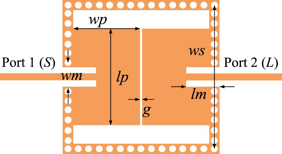
Figure 1 illustrates the structural configuration of the designed dual-band BPF. The device is implemented on an F4B substrate with material parameters of εr = 2.2, tanδ = 0.001, and thickness h = 0.508 mm. The proposed design incorporates: (1) two transversely oriented slots positioned along the upper and lower boundaries of the SIW cavity, (2) a longitudinally aligned slot centered on the symmetry axis, and (3) two quarter-wavelength microstrip resonators integrated in the transverse slot structures. These slot arrangements form two gap-coupled shorted patch resonators operating at the same frequencies. A coplanar waveguide (CPW) transition is employed to realize 50 Ω impedance matching between the feeding ports and the SIW-based filter.
FIGURE 1

Configuration of the proposed dual-band BPF.
2.2 Shorted patch resonator
The proposed dual-band filter achieves broad stopband characteristics primarily through the utilization of shorted patch resonators (the evolutionary process of shorted patches is visualized in Figure 2a). The resonant mode behavior can be analyzed via electric-field distribution along the central symmetry line. Traditional patch resonators exhibit two distinct mode categories: (1) modes with zero tangential electric-field at the centerline, and (2) modes with non-zero tangential electric-field at the centerline. The introduction of an electric wall boundary condition at the centerline exerts differential effects on mode propagation depending on whether the field distribution satisfies the new boundary constraint.
FIGURE 2
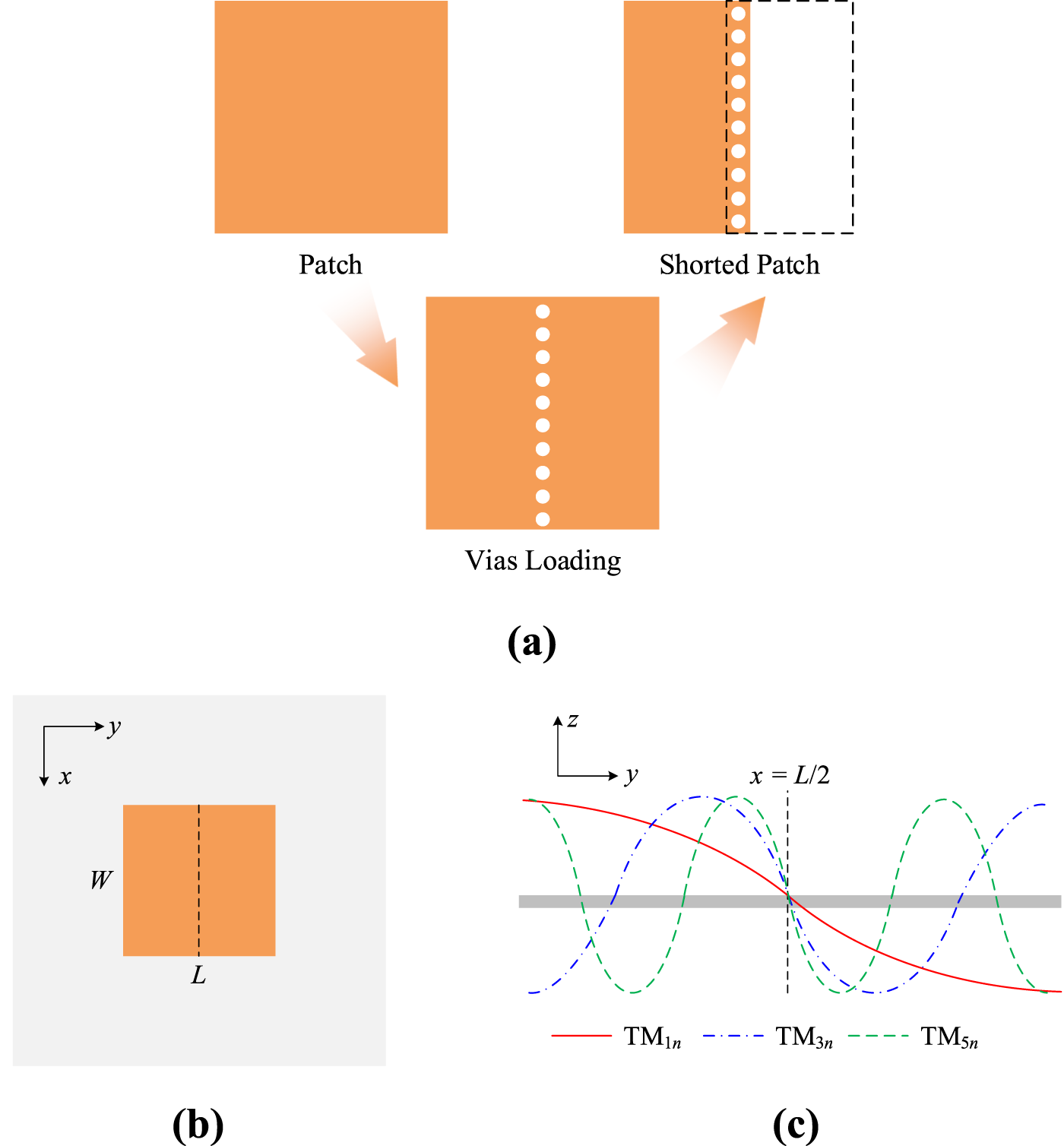
(a) Evolution of shorted patch. (b) Traditional patch configuration. (c) Electric-field of the resonant modes with Ez(x = L/2) = 0.
When truncated to form a shorted resonator, modes with zero tangential electric-field (Et = 0) at the centerline are preserved because their field distributions inherently satisfy the electric wall condition [15]. These modes (e.g., TM10, TM12, TM30) retain their resonant frequencies with minimal perturbation. Conversely, modes featuring non-zero tangential electric-field at the centerline are suppressed due to boundary condition violation. The electric wall enforces Et = 0 at the centerline, which conflicts with the non-zero field requirement of these modes (e.g., TM01, TM20, TM02, TM21, TM22), rendering them non-existent in the shorted configuration.
The mode suppression mechanism can be mathematically validated using the modified Helmholtz equation under electric wall boundary conditions. For a rectangular patch resonator with dimensions L × W (Figure 2b), the TMmn mode resonant frequencies are governed by Equation 1:
In traditional patches, all integer values of m and n are permissible. However, the electric wall at x = L/2 imposes Ez (x = L/2) = 0, restricting valid modes to those with odd m indices. As demonstrated in Figure 2c, only odd m modes (TM1n, TM3n, TM5n…) satisfy the condition sin(mπx/L+90°) = 0 at x = 2/L. Even m modes, which violate this boundary condition, are suppressed. Eigenmode simulations of the shorted patch (Figure 3) confirm that odd-order modes persist in the shorted structure, while even-order modes are eliminated. This mode truncation significantly reduces high-order mode excitation, enabling enhanced stopband performance.
FIGURE 3
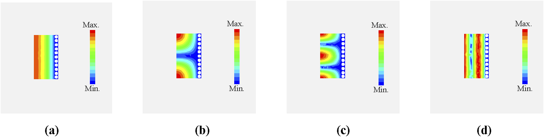
The first four modes in shorted patch resonator. (a) TM10 mode. (b) TM11 mode. (c) TM12 mode. (d) TM30 mode.
2.3 Single-band wide stopband filter
To start with, as depicted in
Figure 4, a single-band BPF is designed by utilizing shorted patch resonators. In an SIW cavity, two gap-coupled shorted patch resonators are realized through the introduction of multiple slots. This single-band BPF is designed to meet the following specifications:
1) Center Frequency (CF): 2.8 GHz;
2) 0-dB Bandwidth (BW): 70 MHz;
3) Return Loss (RL): > 15 dB.
FIGURE 4
Shorted patch-based single-band BPF.
Based on the generalized filter synthesis theory, the coupling matrix of the filter can be obtained as shown in (2):
The external quality factor Qe and inter-resonator coupling coefficient M12 can be extracted using Equations 3, 4Where τS11(fi) denotes the group delay of S11 at resonance fi, f1 and f2 represent coupled resonant frequencies, and f01, f02 are self-resonant frequencies. Figure 5 demonstrates the extracted Qe and M12. Additionally, Figure 6 illustrates the influence of varying some key parameters on the filter response. As shown in Figure 6a, as the value of g increases, the bandwidth of the filter decreases gradually. As shown in Figure 6b, as wp increases, the center frequency of the filter shifts gradually towards lower frequencies.
FIGURE 5
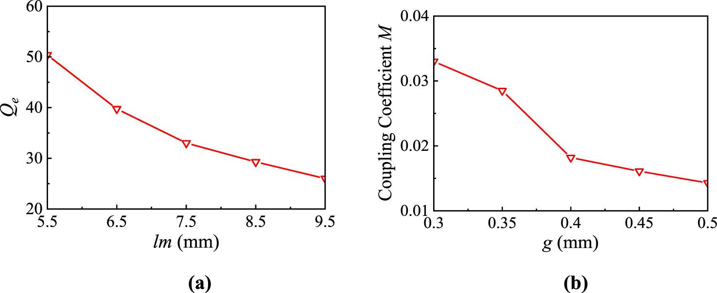
Extracted (a) external quality factor Qe and (b) coupling coefficient M.
FIGURE 6
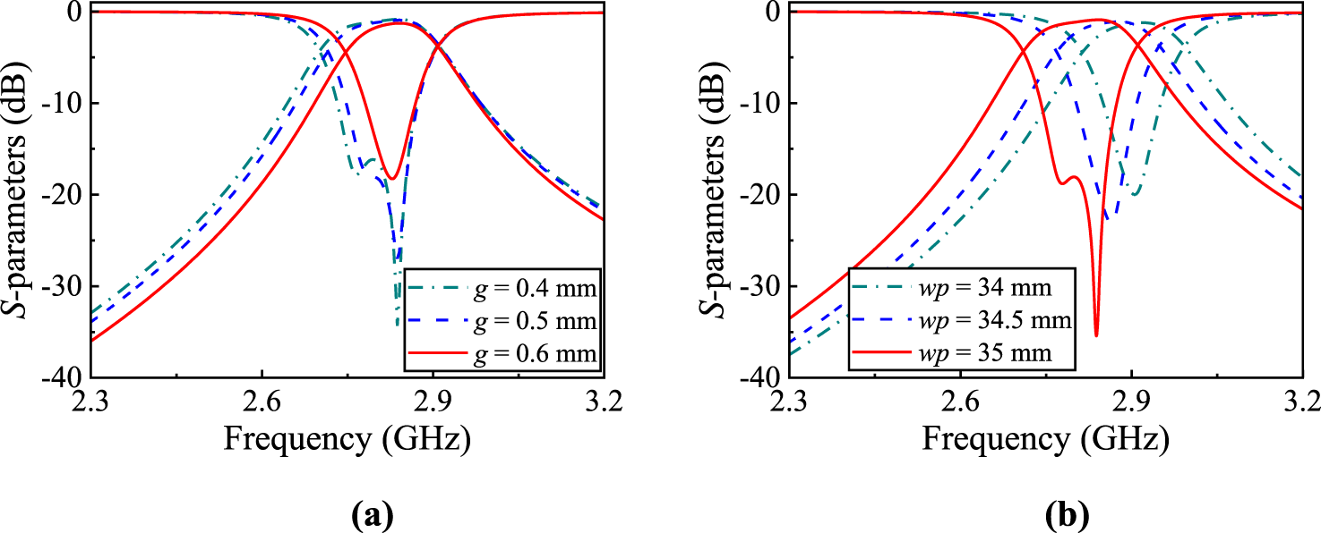
Parameter analysis. (a)g, (b)wp.
Finally, the physical dimensions of the single-band BPF are determined as follows: g = 0.4 mm, wp = 12 mm, lp = 5.66 mm, ws = 14.17 mm, wm = 0.8 mm, lm = 4.4 mm. Figure 7 shows the simulated frequency response, indicating that the filter has a center frequency of 2.8 GHz, a fractional bandwidth (FBW) of 7.2%, and an insertion loss (IL) of 0.83 dB. Additionally, the −20 dB stopband extends to 2.9f0. Figure 8 presents the simulated electric fields in the passband and the spurious-band. It can be observed that the working mode is the TM10 mode, whereas the spurious mode is the TM12 mode.
FIGURE 7
Simulated S-parameters of the single-band BPF.
FIGURE 8
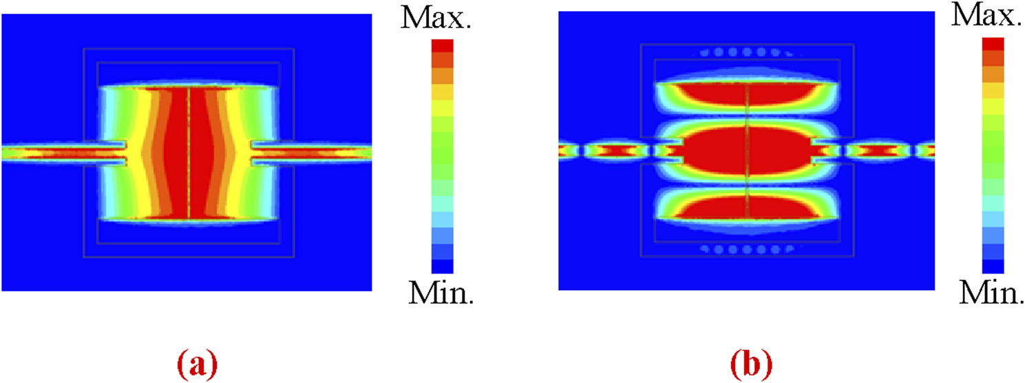
Simulated electric field distributions. (a) 2.8 GHz (Passband). (b) 8.75 GHz (Spurious-band).
2.4 Dual-band wide stopband filter
As shown in Figure 9, two quarter-wavelength resonators are embedded within the upper and lower transverse slots to construct a dual-band filter. The resonant frequency of the quarter-wavelength microstrip resonator is determined by its physical length (cl). The relationship is given by Equation 5:where c is the speed of light in vacuum and εr is the effective permittivity of the microstrip line, accounting for the substrate properties and line geometry. Therefore, tuning the length cl provides direct control over the resonant frequency of the microstrip resonator.
FIGURE 9
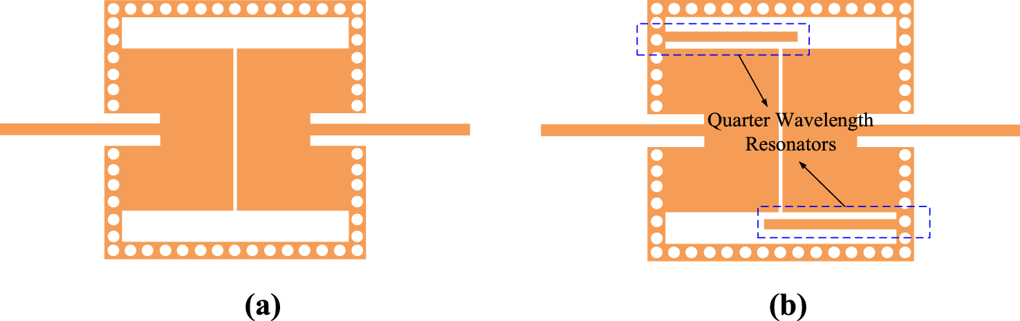
Structure of (a) the single-band design and (b) the dual-band design.
The coupling topologies of the single-band and dual-band filters are illustrated in Figure 10, revealing that the embedded quarter-wavelength resonators act as bandstop sections. By inserting a narrow bandstop segment into the center of the single-pass response, the original passband is split into two separate passbands, resulting in a dual-band response with an extremely small frequency ratio.
FIGURE 10
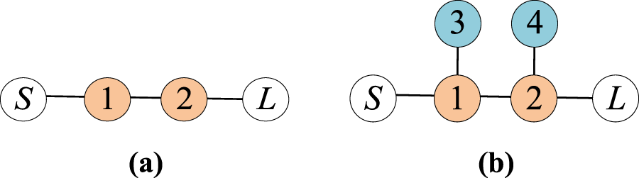
Topology of (a) the single-band design and (b) the dual-band design.
Figure 11a compares the single-band and dual-band responses. Adjusting the length of the quarter-wavelength resonators shifts the resonant frequency of the bandstop section, thereby controlling the BW ratio between the two passbands—an effect clearly evident in Figure 11b. Finally, Figure 12 presents the electric-field distribution of the dual-band filter during operation, effectively demonstrating its operational principle.
FIGURE 11
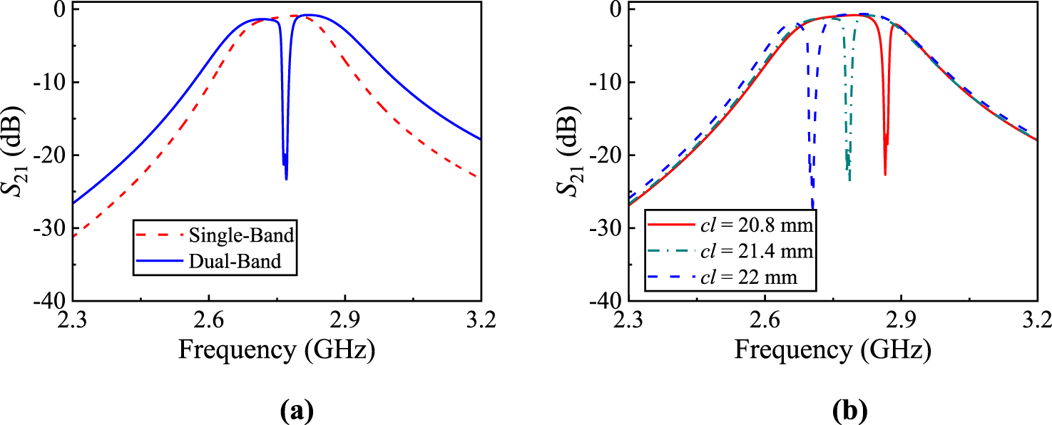
(a) Performance comparison between the single-band design and dual-band design. (b) Bandwidth controllability of the dual-band design.
FIGURE 12
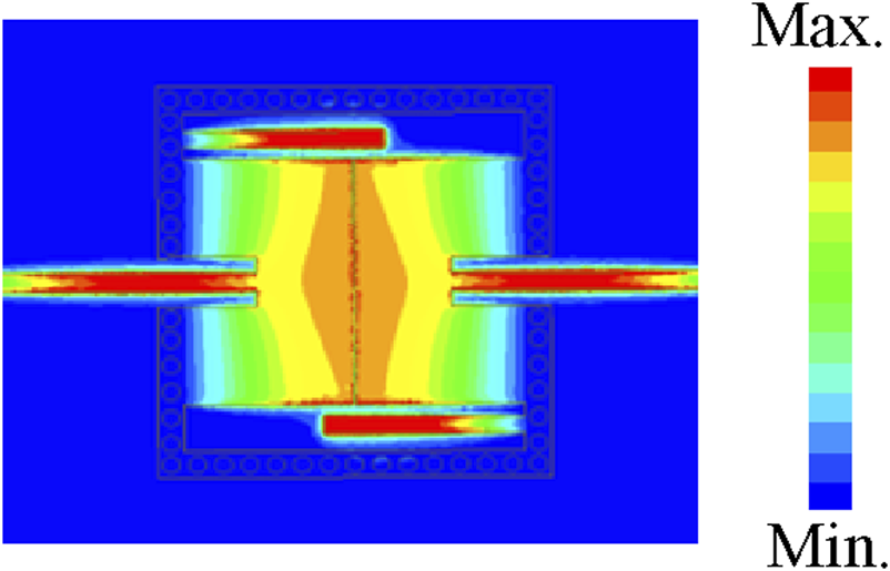
Simulated electric field distributions of the dual-band design.
3 Fabrication and measurement
Based on the design procedure, a dual-band prototype is developed on an F4B substrate with the relative dielectric constant of 2.2, loss tangent 0.001, and the thickness of 0.508 mm. The dimensions are finally determined as follows: wp = 17.4, lp = 23.5, g = 0.2, lm = 9.5, wm = 7, sw = 4.5, cw = 1.5, cl = 19, dl = 1.2, and sl = 32.5 (all units: mm). The fabricated filter occupies a compact size of 0.23 λg2. S-parameters are measured using a ZNB20 vector network analyzer. Figure 13 shows the photograph of the fabricated dual-band BPF.
FIGURE 13
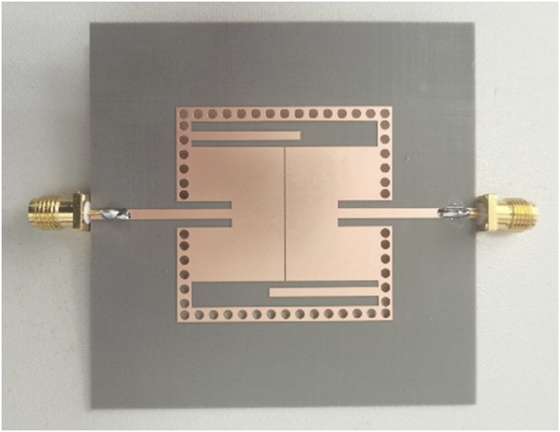
Photograph of the fabricated dual-band BPF prototype.
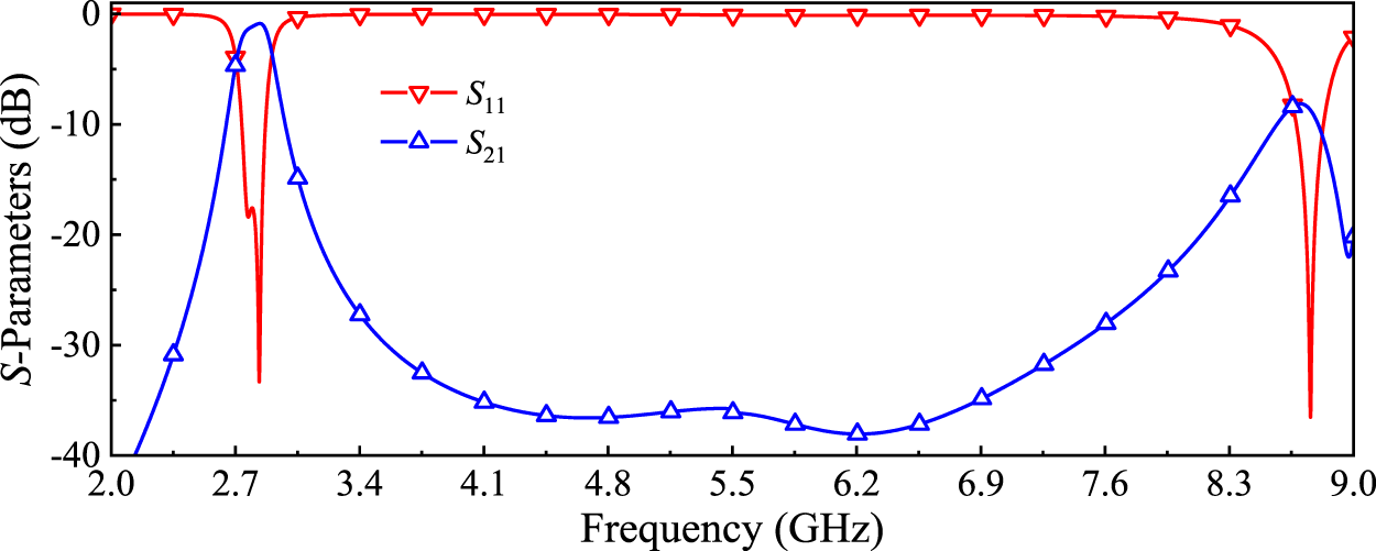
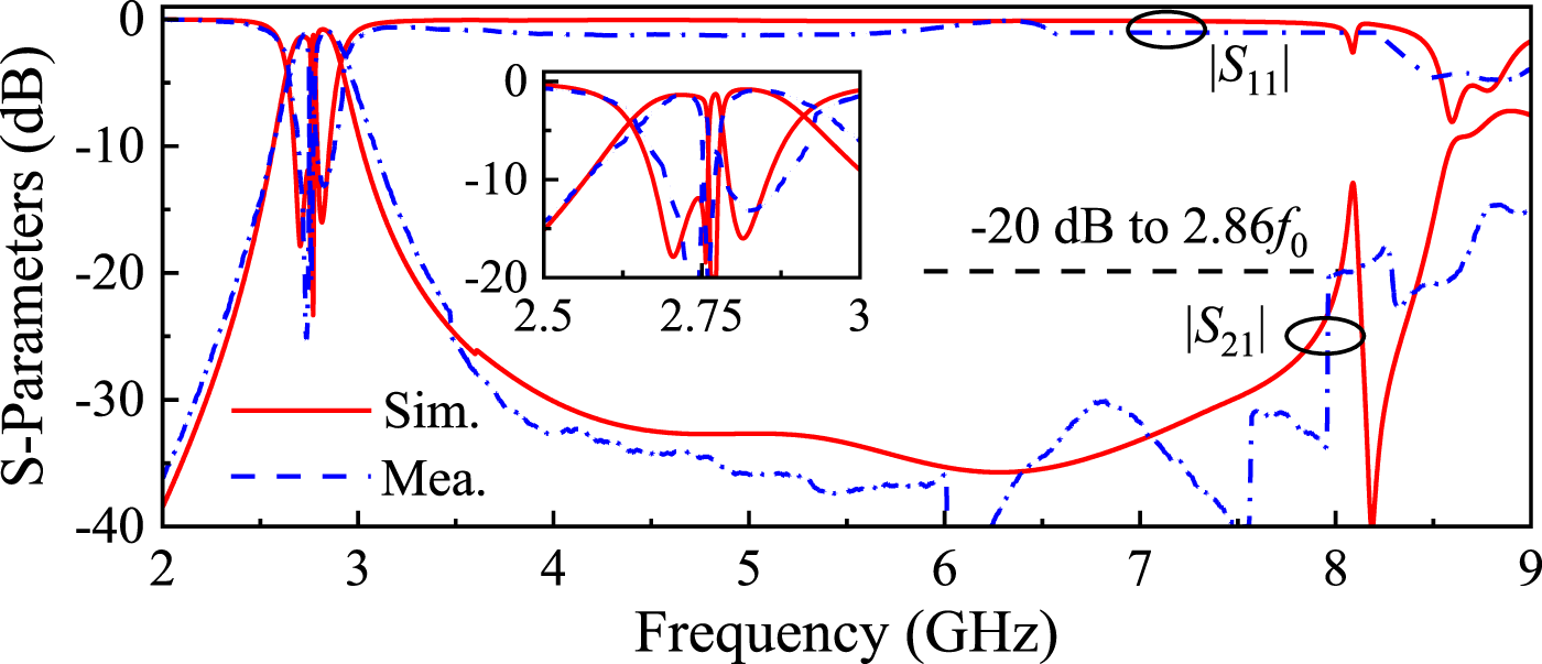
Simulation and measurement results in Figure 14 exhibit good agreement, showing two passbands at 2.71 GHz and 2.83 GHz with 3-dB FBWs of 4.1% and 5.54%, respectively. The measured minimum ILs are 1.3 dB and 0.89 dB, while the −20 dB stopband extends to 2.86f0.
FIGURE 14
Photograph of the fabricated dual-band BPF prototype.
Table 1 compares key metrics with state-of-the-art designs, highlighting the proposed filter’s advantages: more compact size, wider stopband suppression enabled by shorted patches, and an extremely small frequency ratio (1:1.06), validating its superiority for integrated RF applications.
TABLE 1
| References | CF (GHz) | FBW (%) | IL (dB) | Size (λg2) | Rej.(dB)/S.B.(f0) | Freq. ratio |
|---|---|---|---|---|---|---|
| Azad and Mohan [9] | 7.71/9.64 | 5.45/8.1 | 1.9/1.65 | N.A. | N.A. | 1:1.25 |
| Zhang et al. [10] | 3.6/7.1 | 8.2/6.7 | 1.3/1.2 | 0.08 | N.A. | 1:1.97 |
| Zhou et al. [11] | 20/22 | 3.99/5.41 | 1.58/1.25 | 3.86 | N.A. | 1:1.1 |
| This work | 2.71/2.83 | 4.1/5.54 | 1.3/0.89 | 0.23 | 20/2.86 | 1:1.04 |
Comparisons with the state-of-the-art dual-band BPFs.
Iso., isolation; Rej., rejection; S.B., stopband.
4 Conclusion
This work proposes a miniaturized dual-band BPF with closely spaced passbands (1:1.04) and a wide stopband using slots-loaded SIW cavity. By embedding quarter-wavelength resonators in transverse slots, the single passband from shorted patch coupling is split into two narrow passbands. The design achieves a −20 dB stopband up to 2.86f0 due to low harmonic characteristics. A prototype validates the design with good agreement between simulations and measurements, demonstrating its feasibility for compact RF systems.
Statements
Data availability statement
The data that supports the findings of this study are available from the corresponding author upon reasonable request.
Author contributions
YL: Writing – original draft, Formal Analysis, Investigation. JN: Formal Analysis, Writing – original draft, Data curation. SL: Investigation, Methodology, Writing – review and editing. QH: Visualization, Data curation, Writing – review and editing, Formal Analysis. JT: Validation, Visualization, Investigation, Writing – review and editing. NL: Supervision, Validation, Writing – review and editing. TM: Writing – review and editing, Validation, Writing – original draft, Methodology, Investigation, Supervision.
Funding
The author(s) declare that financial support was received for the research and/or publication of this article. This work was supported by the Joint Foundation of Key Laboratory of Shanghai Jiao Tong University-Xidian University, Ministry of Education, under Grant LHJJ/2024-6.
Conflict of interest
The authors declare that the research was conducted in the absence of any commercial or financial relationships that could be construed as a potential conflict of interest.
Generative AI statement
The author(s) declare that no Generative AI was used in the creation of this manuscript.
Publisher’s note
All claims expressed in this article are solely those of the authors and do not necessarily represent those of their affiliated organizations, or those of the publisher, the editors and the reviewers. Any product that may be evaluated in this article, or claim that may be made by its manufacturer, is not guaranteed or endorsed by the publisher.
References
1.
ChenF-CChuQ-X. Novel multistub loaded resonator and its application to high-order dual-band filters. IEEE Trans Microw Theor Techn (2010) 58(6):1551–6. 10.1109/TMTT.2010.2049161
2.
NocellaVPellicciaLTomassoniCSorrentinoR. Miniaturized dual-band waveguide filter using TM dielectric-loaded dual-mode cavities. IEEE Microw Wireless Compon Lett (2016) 26(5):310–2. 10.1109/lmwc.2016.2549181
3.
ZhouMTangXXiaoF. Compact dual band bandpass filter using Novel E-type resonators with controllable bandwidths. IEEE Microw Wireless Compon Lett (2008) 18(12):779–81. 10.1109/lmwc.2008.2007696
4.
HsuC-YChenC-YChuangH-R. Microstrip dual-band bandpass filter design with closely specified passbands. IEEE Trans Microw Theor Techn. (2013) 61(1):98–106. 10.1109/tmtt.2012.2222912
5.
ZhangSZhuL. Compact split-type dual-band bandpass filter based on λ/4 resonators. IEEE Microw Wireless Compon Lett (2013) 23(7):344–6. 10.1109/LMWC.2013.2264659
6.
ChenDZhuLChengC. A novel dual-band bandpass filter with closely spaced passbands. IEEE Microw Wireless Compon Lett (2014) 24(1):38–40. 10.1109/lmwc.2013.2288277
7.
AzadARMohanA. Substrate integrated waveguide dual-band and wide-stopband bandpass filters. IEEE Microw Wireless Compon Lett (2018) 28(8):660–2. 10.1109/lmwc.2018.2844103
8.
XieH-WZhouKZhouC-XWuW. Compact SIW diplexers and dual-band bandpass filter with wide-stopband performances. IEEE Trans Circuits Syst Exp Briefs (2020) 67(12):2933–7. 10.1109/tcsii.2020.2992059
9.
AzadARMohanA. Single- and dual-band bandpass filters using a single perturbed SIW circular cavity. IEEE Microw Wireless Compon Lett (2019) 29(3):201–3. 10.1109/lmwc.2019.2893379
10.
ZhangHKangWWuW. Miniaturized dual-band SIW filters using E-shaped slotlines with controllable center frequencies. IEEE Microw Wireless Compon Lett (2018) 28(4):311–3. 10.1109/lmwc.2018.2811251
11.
ZhouKZhouC-XWuW. Substrate-integrated waveguide dual-band filters with closely spaced passbands and flexibly allocated bandwidths. IEEE Trans Compon Packag Manuf Technol (2018) 8(3):465–72. 10.1109/tcpmt.2018.2793855
12.
ZhouXZhangGZhengJTangWYangJ. SIW filter with adjustable number of passbands using assembled multimode resonant PCBs. IEEE Trans Circuits Syst Exp Briefs (2022) 69(8):3386–9. 10.1109/tcsii.2022.3157713
13.
SunXZhouXLiYGuXXuBTamKWet alMultilayer packaging dual‐band balanced bandpass filter based on dual‐mode substrate integrated waveguide cavities with split‐type topology. IET Microw Antennas Propag (2023) 17(3):200–7. 10.1049/mia2.12320
14.
ZhouXZhangGFengSTamKWZhangZTangWet alDesign of 3-D integrated SIW multiband bandpass filter with split-type extended doublet topology. IEEE Trans Compon Packag Manuf Technol (2022) 12(10):1681–91. 10.1109/tcpmt.2022.3215446
15.
ZhouXZhangGTamK -WLinHZhangZ. Highly selective filtennas with wide-stopband based on multifunctional slots-loaded substrate-integrated cavity. IEEE Trans Antennas Propagation (2024) 72(7):5520–9. 10.1109/tap.2024.3407379
Summary
Keywords
bandpass filter, shorted patch, slots-loaded, substrate integrated waveguide (SIW), wide stopband
Citation
Li Y, Ni J, Li S, Han Q, Tian J, Li N and Ma T (2025) Miniaturized dual-band bandpass filter with closely spaced passbands and wide stopband. Front. Phys. 13:1637651. doi: 10.3389/fphy.2025.1637651
Received
29 May 2025
Accepted
23 June 2025
Published
23 July 2025
Volume
13 - 2025
Edited by
He Zhu, University of Technology Sydney, Australia
Reviewed by
Chen Zhao, Nanjing University of Information Science and Technology, China
Liying Nie, Hefei University of Technology, China
Updates
Copyright
© 2025 Li, Ni, Li, Han, Tian, Li and Ma.
This is an open-access article distributed under the terms of the Creative Commons Attribution License (CC BY). The use, distribution or reproduction in other forums is permitted, provided the original author(s) and the copyright owner(s) are credited and that the original publication in this journal is cited, in accordance with accepted academic practice. No use, distribution or reproduction is permitted which does not comply with these terms.
*Correspondence: Tianye Ma, tianye.ma@foxmail.com
Disclaimer
All claims expressed in this article are solely those of the authors and do not necessarily represent those of their affiliated organizations, or those of the publisher, the editors and the reviewers. Any product that may be evaluated in this article or claim that may be made by its manufacturer is not guaranteed or endorsed by the publisher.