 Binbin Tao1
 Zhengyang Zhu
- 1School of Innovation and Industrial Engineering, Wanjiang Institute of Technology, Maanshan, China
- 2Automotive and Transportation Engineering, Shenzhen Polytechnic University, Shenzhen, Guangdong, China
Following the discovery of graphene, research on two-dimensional (2D) materials has surged. To enhance the performance and broaden the applications of these materials, heterostructures are formed by stacking two different layered materials through van der Waals (vdW) interactions. This study, based on first-principles calculations, explores the intriguing properties of heterostructures made from Zr2CO2, SiC, and GeC monolayers. The results indicate that the Zr2CO2/SiC and Zr2CO2/GeC vdW heterostructures retain their original band structure and exhibit robust thermal stability at 300 K. Additionally, the Zr2CO2/MC heterostructure, with an I-type band alignment, shows promise as a light-emitting device material. Charge transfer between Zr2CO2 and SiC (or GeC) monolayers are obtained as 0.1459 |e| and 0.0425 |e|, respectively. The potential drop across the interface for Zr2CO2/SiC and Zr2CO2/GeC is 6.457 eV and 3.712 eV, respectively. Besides, the Zr2CO2/SiC vdW heterostructure presents excellent carrier mobility along the transport direction (about 3656 cm2 V−1·s–1). These heterostructures exhibit remarkable optical absorption, further demonstrating the potential of Zr2CO2/MC for optoelectronic applications. This study provides valuable theoretical insights for designing photocatalytic and photovoltaic devices using heterostructures.
Introduction
Since graphene was isolated via mechanical exfoliation in 2004 by Novoselov and Geim, its exceptional physical and chemical features have sparked extensive interest in the broader family of 2D materials [1–3]. Many of these exhibit outstanding properties of their own [4, 5]. For instance, black phosphorene, a puckered-layered structure, demonstrates high carrier mobility reaching 1000 cm2/V·s at a thickness of 10 nm and shows great potential for transistors under ambient conditions [6]. The bandgap of arsenene can be tuned through applied strain, even transforming into a direct bandgap semiconductor with just 1% strain [7]. Transition metal dichalcogenides (TMDs), another important 2D family, exhibit desirable optical, thermal, and electronic characteristics [8]. MoS2, for example, offers excellent photodetection capabilities with high responsivity and thermal resilience [9]. Furthermore, Janus-type TMDs break structural symmetry, greatly enhancing carrier mobility and separation efficiency for photogenerated charge carriers, enabling efficient redox processes under light illumination [10–13].
To achieve more complex or application-specific functionalities, researchers often engineer heterostructures by stacking different 2D layers using weak vdW interactions [14–16]. These heterostructures exhibit novel interfacial, optical, and electronic behaviors [17]. For example, SiC-based vdW heterostructures serve as efficient photocatalysts for water splitting [18], and PbSe/CdSe systems exhibit near-infrared emission due to type-I band alignment [19]. In the PbI2/WS2 heterostructure, comparable interlayer diffusion rates of electrons and holes were observed [20]. Such type-I systems hold significant promise in solar energy harvesting, photocatalysis, and optoelectronics [21]. Recently, exfoliated MAX phase derivatives known as MXenes have attracted attention for their diverse properties, ranging from electrical conductivity to chemical stability [22]. Though many MXenes are metallic, some—like Zr2CO2—exhibit semiconducting behavior with advantageous bandgaps. Cr2TiC2, for instance, acts as a bipolar antiferromagnetic semiconductor and may be applied in spintronic devices [23–25]. features high carrier mobility (∼1531.48 cm2/V·s) and promising thermoelectric behavior, making it ideal for photocatalysis and nanoelectronics. Its properties are further tunable via external strain, and its sensitivity to gases like NH3 enables substantial conductivity changes [26]. Similarly, MC monolayers (M = Si, Ge) have recently shown desirable mechanical, optical, and electronic traits, making them candidates for optoelectronic integration [27–29]. Meanwhile, ultrathin SiC is being explored for UV LEDs and laser diodes, while GeC has been synthesized using encapsulated epitaxial techniques and considered for applications in heterojunctions and photocatalysis [30, 31]. Although some heterostructures involving Zr2CO2 or MC have been examined—such as Zr2CO2/WS2, Zr2CO2/blue phosphorene, and MoS2/MC—there remains a lack of research on heterostructures combining Zr2CO2 with MC directly. Given their complementary and tunable properties, forming Zr2CO2/MC heterostructures is a logical step toward realizing advanced multifunctional 2D materials.
This work utilizes density functional theory to evaluate the structural and electronic features of Zr2CO2/MC (M = Si, Ge) heterostructures. We assess their stability via binding energy and ab initio molecular dynamics (AIMD) simulations. Additionally, we characterize their band alignment, charge redistribution, interfacial potential shifts, and light absorption properties, aiming to understand their suitability for optoelectronic applications.
Methods
The calculations in this study are grounded in density functional theory (DFT), carried out using the Vienna Ab initio Simulation Package (VASP) [32, 33]. Exchange–correlation effects were treated within the generalized gradient approximation (GGA) framework, utilizing the Perdew–Burke–Ernzerhof (PBE) functional [34–36]. To achieve more accurate predictions of electronic bandgaps, we employed the hybrid Heyd–Scuseria–Ernzerhof (HSE06) functional [37]. To incorporate van der Waals interactions, the DFT-D3 correction scheme developed by Grimme was applied [38], along with dipole corrections to address long-range dispersion forces. The plane-wave energy cutoff was set at 500 eV following convergence testing. For Brillouin zone sampling, a Monkhorst–Pack k-point mesh of 7 × 7 × 1 was used during structure optimization, whereas denser grids (11 × 11 × 1) were employed for static and optical calculations. A vacuum spacing of 25 Å was introduced along the z-axis to eliminate interlayer interactions arising from periodic boundary conditions. The total energy convergence criterion was set as 10−1 eV, and ionic relaxation was halted when the maximum Hellmann–Feynman force on any atom fell below 0.01 eV Å–1.
Results and discussion
We initially carried out geometry optimizations for monolayered Zr2CO2, SiC, and GeC. Their respective top and side atomic views, along with the calculated band structures, are shown in Figures 1a–c. The optimized lattice constants were determined to be 3.363 Å for Zr2CO2, 3.235 Å for SiC, and 3.096 Å for GeC, agreeing with the previous research [26, 39, 40]. The bond lengths shown as Table 1 include 2.369 Å for Zr–C, 2.132 Å for Zr–O, 1.805 Å for Si–C, and 1.895 Å for Ge–C. Electronic structure calculations using the HSE06 functional confirmed semiconducting behavior for all three monolayers, with corresponding bandgaps of 1.820 eV (Zr2CO2), 4.042 eV (SiC), and 3.354 eV (GeC), which also consistent with previous investigations [41–43]. In the Zr2CO2 monolayer, the conduction band minimum (CBM) lies at the M point, while the valence band maximum (VBM) appears at the Γ point. For SiC and GeC, the CBM and VBM are located at Γ and K points, respectively. These findings are consistent with previous computational results.
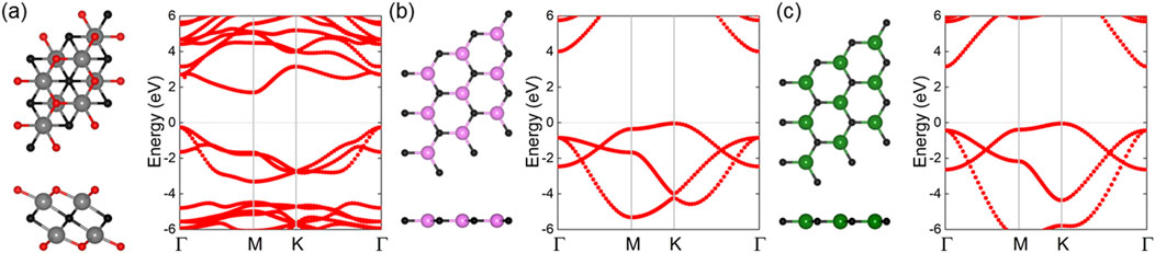
Figure 1. The structure and the HSE06 calculated band structure of the (a) Zr2CO2, (b) SiC and (c) GeC monolayers. The grey, black, red, pink, green balls represent the Zr, C, O, Si and Ge atoms, respectively and the Fermi energy level is 0 shown by gray dashed.
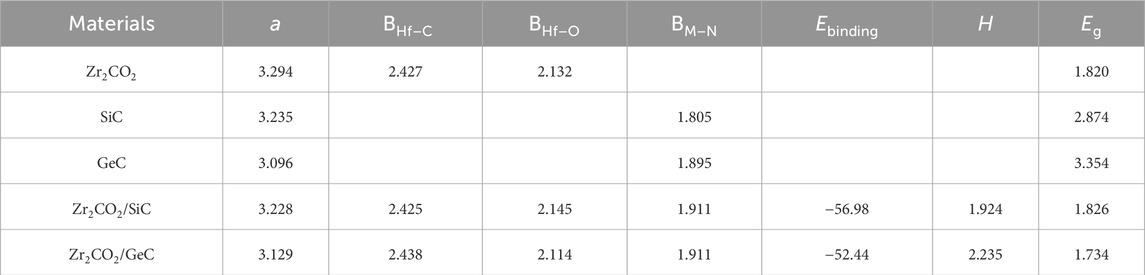
Table 1. The equilibrium lattice constant (a, Å), bond distance (B, Å), binding strength (Eb, meV/Å–2), interfacial separation (H, Å), and electronic bandgap (Eg, eV) for Zr2CO2, SiC, GeC monolayers, as well as for Zr2CO2/SiC and Zr2CO2/GeC heterostructures.
To create heterostructures between Zr2CO2 and MC (M = Si, Ge), six distinct stacking configurations were explored, as illustrated in Figures 2a–f. The binding energy (Eb) for each configuration was calculated using the Equation 1 [44]:
where EZr2CO2/MC, EZr2CO2 and EMC show the total energy of the Zr2CO2/MC heterostructure, monolayered Zr2CO2 and MC, respectively. The smaller binding energy means the more stable structure for the heterostructure. Among the six configurations shwoing as Figures 2a–f, the ZM-1 stacking arrangement exhibited the lowest binding energy, indicating it as the most energetically favorable. For the most stable configuration, the binding energies of the Zr2CO2/SiC and Zr2CO2/GeC heterostructures were found to be −55.69 meV/Å2 and –51.33 meV/Å2, respectively, which is smaller than that in graphites about −18 meV/Å−2, suggesting van der Waals (vdW) interactions between the interface of the Zr2CO2/MC heterostructure [45]. Besides, all the obtained binding energy of the Zr2CO2/SiC and Zr2CO2/GeC heterostructure with different stacking configurations are demonstrated as Supplementary Table S1. As expected, the interfacial bonding does not drastically alter the original intra-layer bond lengths, confirming the weak yet stable coupling. The calculated interface separations are 1.895 Å for Zr2CO2/SiC and 2.254 Å for Zr2CO2/GeC. Henceforth, discussions will focus on these energetically preferred heterostructures.
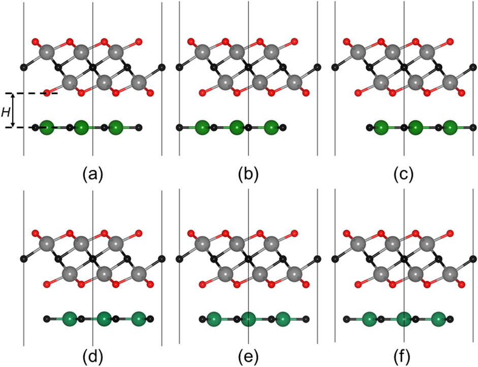
Figure 2. Top and side views of the (a) ZM-1, (b) ZM-2, (c) ZM-3, (d) ZM-4, (e) ZM-5 and (f) ZM-6 stacking configurations of the Hf2CO2/MC heterostructure.
To assess the thermal robustness of the Zr2CO2/MC heterostructures, we performed ab initio molecular dynamics (AIMD) simulations using the Nosé–Hoover thermostat approach [46]. Supercells of size 6 × 6 × 1 were constructed for both Zr2CO2/SiC and Zr2CO2/GeC systems, encompassing a total of 252 atoms. These simulations were carried out at a constant temperature of 300 K for a duration of 10 picoseconds. Post-simulation snapshots of the atomic configurations are displayed in Figures 3a,c, illustrating that both heterostructures maintain structural integrity throughout the simulation. This outcome indicates excellent thermal stability under ambient conditions. Additionally, Figures 3b,d show the fluctuations in total energy as a function of time. The minor oscillations and consistent convergence confirm that the systems reach thermal equilibrium, further validating the reliability of the simulations.
Figure 3. The AIMD simulation results at 300 K over 10 ps, including structural snapshots of (a) Zr2CO2/SiC and (c) Zr2CO2/GeC vdWs heterostructures, along with corresponding energy and temperature profiles shown in (b,d), respectively.
The projected band structures for the Zr2CO2/SiC and Zr2CO2/GeC heterostructures are presented in Figures 4a,c, respectively. These results reveal indirect bandgaps of 2.056 eV for the SiC-based system and 1.902 eV for the GeC-based counterpart. In each case, the colored bands denote the individual contributions from the Zr2CO2 and MC layers, with red and gray representing the MXene and MC monolayers, respectively. Both the conduction band minimum (CBM) and valence band maximum (VBM) are predominantly contributed by the Zr2CO2 layer, indicating a type-I band alignment. This conclusion is further supported by the projected density of states (PDOS) shown in Figures 4b,d, which clearly display dominant contributions from the MXene near the Fermi level. These findings suggest that Zr2CO2/MC heterostructures retain the desirable features of the constituent layers while exhibiting new interfacial properties favorable for light-emitting and optoelectronic devices. Furthermore, the band structures of the Zr2CO2/SiC and Zr2CO2/GeC vdW heterostructures by all six different stacking configurations are obtained in Supplementary Figures S1, S2, respectively, in the Supplementary Material.
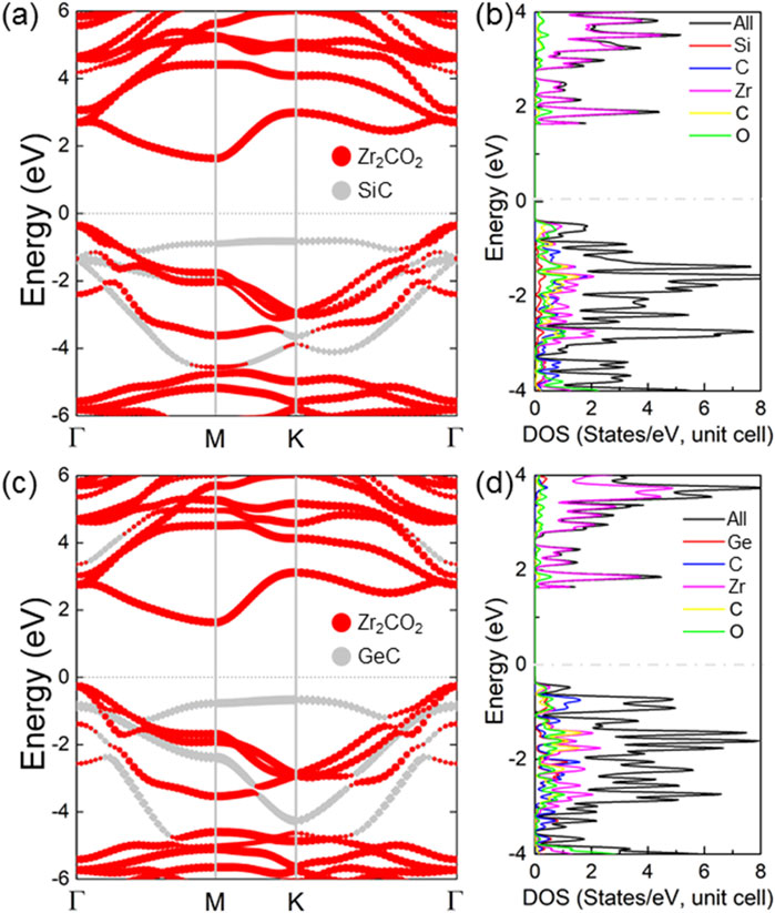
Figure 4. The computed projected band structures for (a) Zr2CO2/SiC and (c) Zr2CO2/GeC van der Waals heterostructures. Corresponding projected density of states are illustrated in (b,d), respectively. The Fermi energy level is set to zero.
In the Zr2CO2/MC heterostructures, the narrower bandgap of the Zr2CO2 layer compared to that of SiC or GeC positions both its CBM and VBM within the wider gap of the MC layers, as illustrated schematically in Figures 5a, b. This energy alignment confirms the presence of a type-I band structure. Under external excitation, electrons in the MC layers are promoted to their CBM, and corresponding holes form at the VBM. Owing to the conduction band offset (CBO) and valence band offset (VBO), these photoexcited carriers migrate from the MC layer to the Zr2CO2 layer. For the Zr2CO2/SiC heterostructure, the CBO and VBO are calculated as 2.458 eV and 1.779 eV, respectively. In the case of Zr2CO2/GeC, these values are 0.447 eV and 0.336 eV. Because the Zr2CO2 layer has a lower potential energy at both band edges, it acts as a well that confines the carriers, thus minimizing their leakage back into the MC layers. This characteristic is advantageous for light-emitting applications, as it facilitates efficient radiative recombination by concentrating electrons and holes in the same material region.
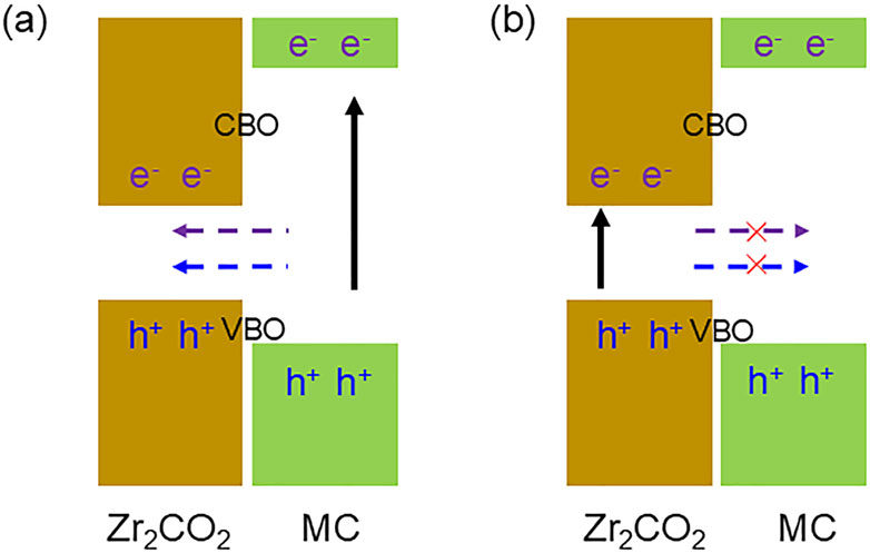
Figure 5. Illustration of charge carrier migration across the interface within the type-I band alignment of the Zr2CO2/MC van der Waals heterostructure with the mechanism of (a) circulation and (b) non connectivity.
Carrier mobility plays a crucial role in developing efficient light-emitting applications. In this work, the electron and hole mobilities of Zr2CO2/MC van der Waals heterostructures are investigated. First, the effective masses (m*) of the electron and hole are decided by fitting the parabolic functions, which can be represented by Equation 2:
where k, Ek are the wave vector and the corresponding electronic energy, respectively. The calculations of carrier mobility (μ) are performed using the Bardeen–Shockley model as Equation 3:
where e,
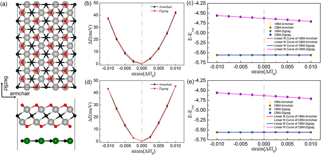
Figure 6. Atomic configurations of the armchair and zigzag terminations in monolayer (a) Zr2CO2/MC vdWs heterostructures. Panels (b,d) illustrate the variation in total energy (ΔE) for orthorhombic Zr2CO2/SiC and Zr2CO2/GeC systems, respectively, under uniaxial strain applied along both armchair and zigzag directions. (c,e) display the evolution of band edge positions for these heterostructures subjected to strain along the same orientations.
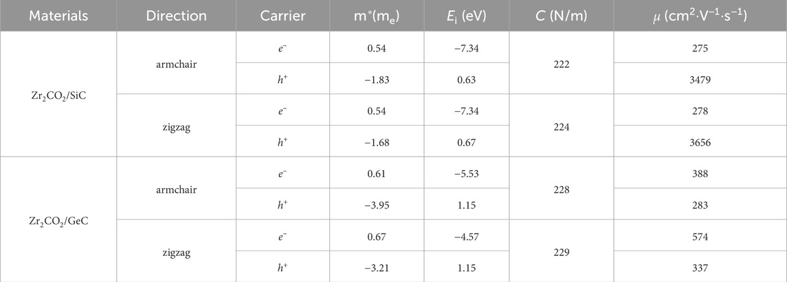
Table 2. Effective mass (m*), elastic modulus (C), deformation potential constant (Ei), and carrier mobility (μ) of the carriers (electron and hole) along the transport directions for the monolayered MoSSe/XN (X = Ga, Al) vdW heterostructure calculated by PBE functional at 300K.
To gain insight into the interfacial electronic interactions, we analyzed the charge redistribution in the Zr2CO2/MC heterostructures. The differential charge density (Δρ) was calculated using the following Equation 4:
where ρMXene/MC, ρMXene and ρMC show the total charge density of the Zr2CO2/SiC (or Zr2CO2/GeC) vdW heterostructure, monolayered Zr2CO2 and SiC (or GeC), respectively. Figures 7a, 6b illustrate the charge distribution at the interfaces of Zr2CO2/SiC and Zr2CO2/GeC. It is evident that both SiC and GeC layers serve as electron donors upon contact, transferring charge to the Zr2CO2 layer. This electron movement leads to the emergence of regions enriched and depleted in charge, forming distinct dipole layers at the interface. Quantitatively, Bader charge analysis reveals that 0.1459 |e| and 0.0425 |e| electrons are transferred from SiC and GeC to the Zr2CO2 layer, respectively. Furthermore, the charge transfer between the Zr2CO2/SiC and Zr2CO2/GeC heterostructures with other stacking structures have been calculated as Supplementary Table S2, one can see that the ZM-1 configuration still results maximum charge transfer. This charge redistribution also induces a potential drop (ΔV) across the interface, calculated to be 6.457 eV for Zr2CO2/SiC and 3.712 eV for Zr2CO2/GeC. Such interfacial potential differences serve as an internal driving force, enhancing carrier transport across the heterostructure.
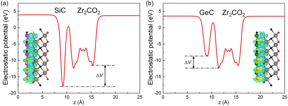
Figure 7. The electrostatic potential profiles at the interface of (a) Zr2CO2/SiC and (b) Zr2CO2/GeC van der Waals heterostructures are illustrated. Yellow regions indicate electron accumulation, while cyan regions represent electron depletion. An isosurface value of 0.0001 |e| has been selected for visualization.
The optical characteristics of the Zr2CO2/MC heterostructures were evaluated through absorption spectrum analysis derived from the complex dielectric function. The absorption coefficient α(ω) was obtained using the Equation 5:
where ω is the angular frequency, c denotes the speed of light, and ε1, ε2 are the real and imaginary parts of the dielectric function, respectively. Furthermore, ε2 (ω) can be calculated by Equation 6 [50]:
where the wave function, energy, and unit vector of the incident light electric field are denoted by
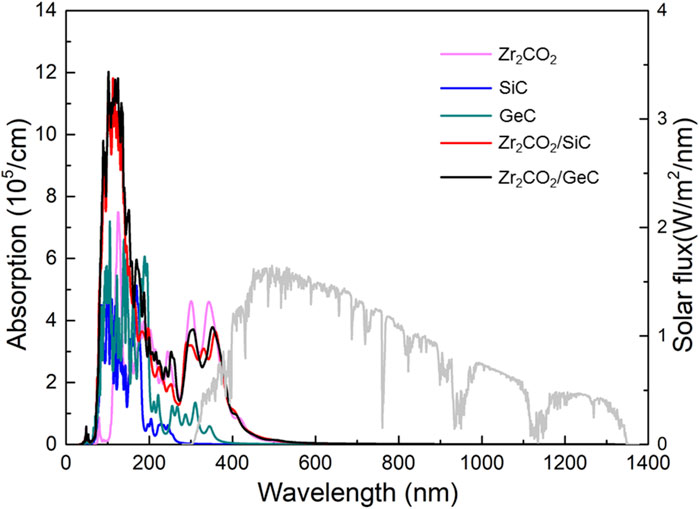
Figure 8. The HSE06 functional obtained optical absorption spectrum for the Zr2CO2, SiC, GeC monolayers and Zr2CO2/SiC, Zr2CO2/GeC vdW heterostructures.
Conclusion
In this work, the structural, electronic, and optical characteristics of monolayer Zr2CO2, SiC, and GeC—as well as their corresponding van der Waals heterostructures—have been comprehensively explored using first-principles calculations. The constructed Zr2CO2/SiC and Zr2CO2/GeC heterostructures demonstrate high thermal resilience, retaining their integrity at 300 K based on ab initio molecular dynamics simulations. These heterostructures exhibit type-I band alignment, with indirect bandgaps of 2.056 eV and 1.902 eV, respectively. The band edges are mainly derived from the Zr2CO2 layer, positioning these systems as promising candidates for light-emitting applications. Interlayer charge transfer was observed, with calculated electron donation from the MC layers of 0.1459 |e| (SiC) and 0.0425 |e| (GeC), inducing interfacial potential drops of 6.457 eV and 3.712 eV. These potential differences facilitate efficient carrier transport across the interface. Additionally, both heterostructures display significantly improved optical absorption, particularly across visible and near-infrared wavelengths, outperforming their monolayer counterparts. These optical features support the use of Zr2CO2/MC systems in energy-related optoelectronic technologies.
Data availability statement
The original contributions presented in the study are included in the article/Supplementary Material, further inquiries can be directed to the corresponding authors.
Author contributions
BT: Validation, Writing – review and editing, Writing – original draft, Visualization, Data curation, Resources. ZZ: Writing – review and editing, Resources, Data curation, Validation. JL: Software, Investigation, Funding acquisition, Writing – review and editing, Supervision.
Funding
The author(s) declare that financial support was received for the research and/or publication of this article. All authors thank the Anhui Province Higher Education Science Research Project Funding (2022AH052432), the research Projects of Department of Education of Guangdong Province (2024ZDZX3081) and Shenzhen Polytechnic Research Fund (6023310003K).
Conflict of interest
The authors declare that the research was conducted in the absence of any commercial or financial relationships that could be construed as a potential conflict of interest.
Generative AI statement
The author(s) declare that no Generative AI was used in the creation of this manuscript.
Publisher’s note
All claims expressed in this article are solely those of the authors and do not necessarily represent those of their affiliated organizations, or those of the publisher, the editors and the reviewers. Any product that may be evaluated in this article, or claim that may be made by its manufacturer, is not guaranteed or endorsed by the publisher.
Supplementary material
The Supplementary Material for this article can be found online at: https://www.frontiersin.org/articles/10.3389/fphy.2025.1655987/full#supplementary-material
References
2. Novoselov KS, Mishchenko A, Carvalho A, Castro Neto AH. 2D materials and van der Waals heterostructures. Science (2016) 353:aac9439. doi:10.1126/science.aac9439
3. Miro P, Audiffred M, Heine T. An atlas of two-dimensional materials. Chem Soc Rev (2014) 43:6537–54. doi:10.1039/c4cs00102h
4. Fan Q, Yan L, Tripp MW, Krejčí O, Dimosthenous S, Kachel SR, et al. Biphenylene network: a nonbenzenoid carbon allotrope. Science (2021) 372:852–6. doi:10.1126/science.abg4509
5. Jariwala D, Sangwan VK, Lauhon LJ, Marks TJ, Hersam MC. Carbon nanomaterials for electronics, optoelectronics, photovoltaics, and sensing. Chem Soc Rev (2013) 42:2824–60. doi:10.1039/c2cs35335k
6. Xiao J, Long M, Zhang X, Ouyang J, Xu H, Gao Y. Theoretical predictions on the electronic structure and charge carrier mobility in 2D phosphorus sheets. Scientific Rep (2015) 5:9961. doi:10.1038/srep09961
7. Vishnoi P, Mazumder M, Pati SK, Rao CR. Arsenene nanosheets and nanodots. J New J Chem (2018) 42:14091–5. doi:10.1039/c8nj03186j
8. Zhang H, Chhowalla M, Liu Z. 2D nanomaterials: graphene and transition metal dichalcogenides. Chem Soc Rev (2018) 47:3015–7. doi:10.1039/c8cs90048e
9. Ren K, Sun M. Thermal transport in 2D materials. J Appl Phys (2025) 137:130402. doi:10.1063/5.0267691
10. Ren K, Qin H, Liu H, Chen Y, Liu X, Zhang G. Manipulating interfacial thermal conduction of 2D janus heterostructure via a thermo-mechanical coupling. Adv Funct Mater (2022) 32:2110846. doi:10.1002/adfm.202110846
11. Radisavljevic B, Radenovic A, Brivio J, Giacometti V, Kis A. Single-layer MoS2 transistors. Nat nanotechnology (2011) 6:147–50. doi:10.1038/nnano.2010.279
12. Ren K, Wang F, Liu T, Qin H, Jing Y. Wrinkles in 2D TMD heterostructures: unlocking enhanced hydrogen evolution reaction catalysis. J Mater Chem A (2025) 13:20859–67. doi:10.1039/d5ta00681c
13. Ren K, Wang K, Luo Y, Sun M, Altalhi T, Yakobson BI, et al. Ultralow Frequency Interlayer Mode from Suppressed van der Waals Coupling in Polar Janus SMoSe/SWSe Heterostructure. Mater Today Phys (2025) 53:101689. doi:10.1016/j.mtphys.2025.101689
14. Lee CH, Lee GH, van der Zande AM, Chen W, Li Y, Han M, et al. Atomically thin p-n junctions with van der Waals heterointerfaces. Nat nanotechnology (2014) 9:676–81. doi:10.1038/nnano.2014.150
15. Butler SZ, Hollen SM, Cao L, Cui Y, Gupta JA, Gutiérrez HR, et al. Progress, challenges, and opportunities in two-dimensional materials beyond graphene. ACS nano (2013) 7:2898–926. doi:10.1021/nn400280c
16. Shu H, Wang F, Ren K, Guo J. Strain-tunable optoelectronic and photocatalytic properties of 2D GaN/MoSi2P4 heterobilayers: potential optoelectronic/photocatalytic materials. Nanoscale (2025) 17:3900–9. doi:10.1039/d4nr04545a
17. Zhang C, Ren K, Wang S, Luo Y, Tang W, Sun M. Recent progress on two-dimensional van der Waals heterostructures for photocatalytic water splitting: a selective review. J Phys Phys D Appl Phys (2023) 56:483001. doi:10.1088/1361-6463/acf506
18. Vo TQ, Kim B. Interface thermal resistance between liquid water and various metallic surfaces. Int J Precision Eng Manufacturing (2015) 16:1341–6. doi:10.1007/s12541-015-0176-0
19. Yamaoka T, Lim HE, Koirala S, Wang X, Shinokita K, Maruyama M, et al. Efficient photocarrier transfer and effective photoluminescence enhancement in type I monolayer MoTe2/WSe2 heterostructure. Adv Funct Mater (2018) 28:1801021. doi:10.1002/adfm.201801021
20. Zheng W, Zheng B, Jiang Y, Yan C, Chen S, Liu Y, et al. Probing and Manipulating Carrier Interlayer Diffusion in van der Waals Multilayer by Constructing Type-I Heterostructure. Nano Lett (2019) 19:7217–25. doi:10.1021/acs.nanolett.9b02824
21. Bellus MZ, Li M, Lane SD, Ceballos F, Cui Q, Zeng XC, et al. Type-I van der Waals heterostructure formed by MoS2 and ReS2 monolayers. Nanoscale Horiz (2017) 2:31–6. doi:10.1039/c6nh00144k
22. Liang Q, Zhang Q, Zhao X, Liu M, Wee AT. Defect engineering of two-dimensional transition-metal dichalcogenides: applications, challenges, and opportunities. ACS Nano (2021) 15:2165–81. doi:10.1021/acsnano.0c09666
23. He J, Ding G, Zhong C, Li S, Li D, Zhang G. Cr2TiC2-based double MXenes: novel 2D bipolar antiferromagnetic semiconductor with gate-controllable spin orientation toward antiferromagnetic spintronics. Nanoscale (2018) 11:356–64. doi:10.1039/c8nr07692h
24. Wang K, He J, Zhang M, Wang H, Zhang G. Magnon-phonon interaction in antiferromagnetic two-dimensional MXenes. Nanotechnology (2020) 31:435705. doi:10.1088/1361-6528/aba4cf
25. Sun M, Schwingenschlögl U. Structure prototype outperforming MXenes in stability and performance in metal-ion batteries: a high throughput study. Adv Energy Mater (2021) 11:2003633. doi:10.1002/aenm.202003633
26. He Y, Zhang M, Shi J-j., Cen Y-l., Wu M. Improvement of visible-light photocatalytic efficiency in a novel InSe/Zr2CO2 heterostructure for overall water splitting. J Phys Chem C (2019) 123:12781–90. doi:10.1021/acs.jpcc.9b01175
27. Huang L, Ren K, Zhang H, Qin H. Enhanced mechanical and thermal properties of two-dimensional SiC and GeC with temperature and size dependence. Chin Phys B (2023) 32:076103. doi:10.1088/1674-1056/acc78f
28. Lou P, Lee JY. GeC/GaN vdW heterojunctions: a promising photocatalyst for overall water splitting and solar energy conversion. ACS Appl Mater Inter (2020) 12:14289–97. doi:10.1021/acsami.9b20175
29. Huang L, Zhang YF, Zhang YY, Xu W, Que Y, Li E, et al. Sequence of silicon monolayer structures grown on a Ru surface: from a herringbone structure to silicene. Nano Lett (2017) 17:1161–6. doi:10.1021/acs.nanolett.6b04804
30. Liu Q, Li L, Li Y, Gao Z, Chen Z, Lu J. Tuning electronic structure of bilayer MoS2 by vertical electric field: a first-principles investigation. J Phys Chem C (2012) 116:21556–62. doi:10.1021/jp307124d
31. Ren K, Ren C, Luo Y, Xu Y, Yu J, Tang W, et al. Using van der Waals heterostructures based on two-dimensional blue phosphorus and XC (X= Ge, Si) for water-splitting photocatalysis: a first-principles study. Phys Chem Chem Phys (2019) 21:9949–56. doi:10.1039/c8cp07680d
32. Capelle K. A bird's-eye view of density-functional theory. Braz J Phys (2006) 36:1318–43. doi:10.1590/s0103-97332006000700035
33. Van de Walle CG, Martin RM. Absolute’’deformation potentials: formulation and ab initio calculations for semiconductors. Phys Rev Lett (1989) 62:2028–31. doi:10.1103/physrevlett.62.2028
34. Grest G, Nagel S, Rahman A, Witten T. Density of states and the velocity autocorrelation function derived from quench studies. J Chem Phys (1981) 74:3532–4. doi:10.1063/1.441508
35. Kresse G, Furthmüller J. Efficient iterative schemes for ab initio total-energy calculations using a plane-wave basis set. Phys Rev B (1996) 54:11169–86. doi:10.1103/physrevb.54.11169
36. Sanville E, Kenny SD, Smith R, Henkelman G. Improved grid-based algorithm for bader charge allocation. J Comput Chem (2007) 28:899–908. doi:10.1002/jcc.20575
37. Heyd J, Scuseria GE, Ernzerhof M. Hybrid functionals based on a screened coulomb potential. J Chem Phys (2003) 118:8207–15. doi:10.1063/1.1564060
38. Grimme S, Antony J, Ehrlich S, Krieg H. A consistent and accurate ab initio parametrization of density functional dispersion correction (DFT-D) for the 94 elements H-Pu. J Chem Phys (2010) 132:154104. doi:10.1063/1.3382344
39. Shu H. Adjustable electro-optical properties of novel graphene-like SiC2via strain engineering. Appl Surf Sci (2021) 559:149956. doi:10.1016/j.apsusc.2021.149956
40. Wang G, Zhang L, Li Y, Zhao W, Kuang A, Li Y, et al. Biaxial strain tunable photocatalytic properties of 2D ZnO/GeC heterostructure. J Phys Phys D Appl Phys (2020) 53:015104. doi:10.1088/1361-6463/ab440e
41. Drissi LB, Ramadan FZ, Kanga NBJ. Optoelectronic properties in 2D GeC and SiC hybrids: DFT and many body effect calculations. Mater Res Express (2018) 5:015061. doi:10.1088/2053-1591/aaa862
42. Lü T-Y, Liao X-X, Wang H-Q, Zheng J-C. Tuning the indirect–direct band gap transition of SiC, GeC and SnC monolayer in a graphene-like honeycomb structure by strain engineering: a quasiparticle GW study. J Mater Chem (2012) 22:10062. doi:10.1039/c2jm30915g
43. Zhu XT, Xu Y, Cao Y, Zhao YQ, Sheng W, Nie G-Z, et al. Investigation of the electronic structure of two-dimensional GaN/Zr2CO2 hetero-junction: type-II band alignment with tunable bandgap. Appl Surf Sci (2021) 542:148505. doi:10.1016/j.apsusc.2020.148505
44. Ren K, Sun M, Luo Y, Wang S, Yu J, Tang W. First-principle study of electronic and optical properties of two-dimensional materials-based heterostructures based on transition metal dichalcogenides and boron phosphide. Appl Surf Sci (2019) 476:70–5. doi:10.1016/j.apsusc.2019.01.005
45. Chen X, Tian F, Persson C, Duan W, Chen NX. Interlayer interactions in graphites. Scientific Rep (2013) 3:3046. doi:10.1038/srep03046
46. Nosé S. A unified formulation of the constant temperature molecular dynamics methods. J Chem Phys (1984) 81:511–9. doi:10.1063/1.447334
47. Cai Y, Zhang G, Zhang YW. Polarity-reversed robust carrier mobility in monolayer MoS2 nanoribbons. J Am Chem Soc (2014) 136:6269–75. doi:10.1021/ja4109787
48. Kumar R, Das D, Singh AK. C2N/WS2 van der Waals type-II heterostructure as a promising water splitting photocatalyst. J Catal (2018) 359:143–50. doi:10.1016/j.jcat.2018.01.005
49. Xiao J, Long M, Deng C-S, He J, Cui L-L, Xu H. Electronic structures and carrier mobilities of blue phosphorus nanoribbons and nanotubes: a first-principles study. J Phys Chem C (2016) 120:4638–46. doi:10.1021/acs.jpcc.5b12112
50. Zhang G, Yu M-B, Tung C-H, Lo G-Q. Quantum size effects on dielectric constants and optical absorption of ultrathin silicon films. IEEE Electron Device Lett (2008) 29:1302–5. doi:10.1109/led.2008.2005651
51. Ren K, Zheng R, Yu J, Sun Q, Li J. Band bending mechanism in CdO/Arsenene heterostructure: a potential direct Z-scheme photocatalyst. Front Chem (2021) 9:788813. doi:10.3389/fchem.2021.788813
52. Shao C, Ren K, Huang Z, Yang J, Cui Z. Two-Dimensional PtS2/MoTe2 van der Waals Heterostructure: an Efficient Potential Photocatalyst for Water Splitting. Front Chem (2022) 10:847319. doi:10.3389/fchem.2022.847319
Keywords: 2D materials, heterostructure, first-principles calculation, band structure, application
Citation: Tao B, Zhu Z and Li J (2025) First principles study on the electronic and optical behavior of atomically thin MXene/MC (M = Si, Ge) heterostructures. Front. Phys. 13:1655987. doi: 10.3389/fphy.2025.1655987
Received: 29 June 2025; Accepted: 23 July 2025;
Published: 13 October 2025.
Edited by:
Guangzhao Wang, Yangtze Normal University, ChinaReviewed by:
Longfei Yang, Nanjing University of Science and Technology, ChinaKe Wang, Xi’an University of Posts and Telecommunications, China
Copyright © 2025 Tao, Zhu and Li. This is an open-access article distributed under the terms of the Creative Commons Attribution License (CC BY). The use, distribution or reproduction in other forums is permitted, provided the original author(s) and the copyright owner(s) are credited and that the original publication in this journal is cited, in accordance with accepted academic practice. No use, distribution or reproduction is permitted which does not comply with these terms.
*Correspondence: Jianping Li, c3p5bGpwMDE3MEBzenB1LmVkdS5jbg==