 Nobuyoshi Koshida1*
 Toshihiro Nakamura2
- 1Graduate School of Engineering, Tokyo University of Agriculture and Technology, Fuchu, Japan
- 2Department of Electrical and Electronic Engineering, Hosei University, Tokyo, Japan
Recent topics of application studies on porous silicon (PS) are reviewed here with a focus on the emissive properties of visible light, quasiballistic hot electrons, and acoustic wave. By exposing PS in solvents to pulse laser, size-controlled nc-Si dot colloids can be formed through fragmentation of the PS layer with a considerably higher yield than the conventional techniques such as laser ablation of bulk silicon and sol-gel precursor process. Fabricated colloidal samples show strong visible photoluminescence (~40% in quantum efficiency in the red band). This provides an energy- and cost-effective route for production of nc-Si quantum dots. A multiple-tunneling transport mode through nc-Si dot chain induces efficient quasiballistic hot electron emission from an nc-Si diode. Both the efficiency and the output electron energy dispersion are remarkably improved by using monolayer graphene as a surface electrode. Being a relatively low operating voltage device compatible with silicon planar fabrication process, the emitter is applicable to mask-less parallel lithography under an active matrix drive. It has been demonstrated that the integrated 100 × 100 emitter array is useful for multibeam lithography and that the selected emission pattern is delineated with little distortion. Highly reducing activity of emitted electrons is applicable to liquid-phase thin film deposition of metals (Cu) and semiconductors (Si, Ge, and SiGe). Due to an extremely low thermal conductivity and volumetric heat capacity of nc-Si layer, on the other hand, thermo-acoustic conversion is enhanced to a practical level. A temperature fluctuation produced at the surface of nc-Si layer is quickly transferred into air, and then an acoustic wave is emitted without any mechanical vibrations. The non-resonant and broad-band emissivity with low harmonic distortions makes it possible to use the emitter for generating audible sound under a full digital drive and reproducing complicated ultrasonic communication calls between mice.
Introduction
As the scaling of integrated silicon devices approaches 10 nm or below, precise control of the physical and chemical properties of silicon becomes very important. In the quantum-size region of silicon (<4.7 nm), particularly, optimal processing is critical to enhance the optical, electrical, thermal, interfacial, and mechanical properties. Porous silicon (PS), prepared by electrochemical anodization of crystalline silicon (c-Si) under the certain conditions, consists of a nanopore structure and residual quantum-sized nanocrystalline silicon (nc-Si). With appropriate surface passivation, nc-Si shows tunable properties in different ways from those of bulk c-Si and plays a role as a platform of functional devices in photonics, electronics, biometrics, biomedicine, acoustics, energetics, and so on (Sailor, 2012; Canham, 2017). From among these possibilities, the studies on the emission of photons, electrons, and ultrasound are discussed here.
Regarding the photonic applications, one key issue is to develop an efficient fabrication process of highly luminescent nc-Si colloids. For this purpose, some top-down and bottom-up approaches have been conducted to obtain colloidal nc-Si dots (Heath, 1992; Henderson et al., 2009; Shirahata et al., 2010). Typical techniques in the former are laser ablation of c-Si wafer and ultrasonic fragmentation of PS. Those in the latter are chemical vapor deposition (CVD), thermal decomposition treatment, and liquid-phase chemical reaction. In any case, an energy- and cost-effective process is strongly required for producing a practical amount of nc-Si dots or powder. Although the complicated nanostructure in PS layers seems to impede the electrical conduction, on the other hand, experimental and theoretical analyses of electron transport in arrayed nc-Si dots suggests the existence of a specific multiple-tunneling cascade mode therein (Koshida, 2017a). This leads to quasiballistic electron emission from an nc-Si diode. Its usefulness has been demonstrated not only in vacuum but also in atmospheric-pressure gases and solutions. Due to extremely low thermal conductivity and volumetric heat capacity of the nc-Si layer (Lysenko et al., 1999; Valalaki and Nassiopoulou, 2013, 2014, 2017; Koshida, 2017b), in addition, thermo-acoustic coupling with air is enhanced. Since no mechanical vibrations are involved, this thermally induced sound emission shows non-resonant flat frequency response (Koshida, 2017c). The nc-Si sound source can effectively reproduce complicated ultrasonic communication calls between mice.
These functional applications are different from the pursuit of scaling merits that have been sought in usual silicon device technology. The present status of technological exploration is summarized in the following sections and some recent developments are highlighted.
Diversifying Studies of Porous Silicon
While the minimum size of advanced large-scale integrated (LSI) circuit enters into the region below 10 nm, another viewpoint relating to environmental, social, and human issues has become important in pursuing the silicon device technology. Actually, the International Technology Roadmap for Semiconductors was recently reorganized1 such that some new intentionality and keywords are contained [such as systems, beyond CMOS (complementary metal-oxide-semiconductor) logic, emerging research materials, and so on] in addition to the conventional scaling activity “more Moore.” The silicon technology has reached the phase of evolutionary transformation from straightforward scaling to diversification, systematization, and functional combinations.
The scientific and technological evolution of PS materials is shown in Figure 1. Reflecting the versatile structures of PS, its research and development (R&D) have been conducted in many divergences. In the early stage just after finding of PS by Uhlir (1956), the interests of PS were mainly in the formation mechanism and structural characterizations (Lehman, 2002). The application studies were field oxide formation for integrated device isolation (Watanabe et al., 1975) and use as substrates for epitaxial growth of compound and elemental semiconductors (Lin et al., 1987). Discovery of visible photoluminescence by Canham (1990) at 1990 led to the expansion of concern from the use as passive components to as an active quantum confinement material. Related investigations were also reported around that time on the photoelectrochemical solar cell (Koshida et al., 1985), photoconduction (Koshida et al., 1991), and electroluminescence (Koshida and Koyama, 1992), and optical effects (Thonissen et al., 1997). It was clarified that the physical and chemical properties of PS become radically different from those of single-crystalline bulk silicon. Then, the continuing studies paved the way for advanced surface chemistry (Coffinier and Boukherroub, 2016), biocompatibility (Canham, 1995), bio-sensors (Lin et al., 1997), biomedical therapy (Santos, 2014), quasiballistic electron emission (Koshida et al., 1999), thermal isolation (Nassiopoulou and Kaltsas, 2000; Nassiopoulou, 2014), and thermoacoustics (Shinoda et al., 1999). Recently the studies are further expanded to the field of energetics (Kouassi et al., 2012). Tunable optical, electrical, structural, surface, thermal, and chemical properties of PS meet the above-mentioned situation that silicon technology is rapidly evolving in a multilateral manner.
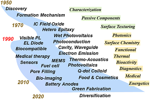
Figure 1. Evolution of research and development activities in nanostructured porous silicon.
Emissive Properties and Applications
Visible Luminescent Quantum Dots
Bottom-Up Fabrication Routes of Silicon Quantum Dot
Free-standing mono-dispersed colloidal particles of nc-Si (nc-Si dots) with diameter range of ~2–8 nm is well known to exhibit size-tunable visible luminescence. Both the dispersibility of nc-Si dots in solution and luminescence properties can be controlled by modifying their surface termination (Dohnalová et al., 2014). Recently, because of such interesting properties and the resultant compatibility of future solution-based luminescence devices, such as flexible electroluminescence diode (Choi et al., 2018), the nc-Si dot attracts a lot of attention. In addition, silicon dots are expected to apply in bio-technology, such as cellular imaging, due to non-toxicity of silicon (Cheng et al., 2014). For these applications, scalable production routes of the luminescent nc-Si dots are expected to develop. In this section, we review various routes for the nc-Si dots formation and the recent advances in the efficient production of the nc-Si dots, including the processes where PS (an assembly of nc-Si dots) is utilized as an intermediate material.
The nc-Si dots are prepared through the two types of preparation routes, i.e., top-down and bottom-up routes as summarized in Figure 2. A typical bottom-up process is the solution-phase chemical synthesis (Heath, 1992; Wilcoxon et al., 1999; Holmes et al., 2001; English et al., 2002; Zou et al., 2004; Liu et al., 2005; Dohnalová et al., 2012, 2013; Cheng et al., 2015; Debenedetti et al., 2015; Ghosh et al., 2018). In this method, the reduction of silicon precursors, such as SiCl4 with Zintl salts (KSi, NaSi, Mg2Si), at high temperature under high pressures forms colloidal nanocrystals. To render soluble the silicon colloids in arbitrary solvents (polar or nonpolar solvents), their surface termination usually modifies from initial termination (e.g., Br and Cl) to organic ligands. In some cases, further ligand exchanges from a ligand (e.g., alkene and thiol groups) to another ligand or biomolecules were performed for the organically-capped silicon colloids (Shiohara et al., 2010; Ruizendaal et al., 2011). The prepared colloids usually exhibit an emission in blue to green regions with nanosecond lifetimes, indicating the surface-related or direct gap recombination (Holmes et al., 2001; Dohnalová et al., 2012, 2013). Furthermore, by attaching adequate surface ligands, yellow to red luminescent colloids can be obtained. Interestingly their luminescent quantum efficiency increases up to ~90% (Qi et al., 2016). Note that the quantum efficiencies of typical nc-Si dots, where the quasi-direct electron-hole recombination occurs, were up to 60% (Jurbergs et al., 2006).
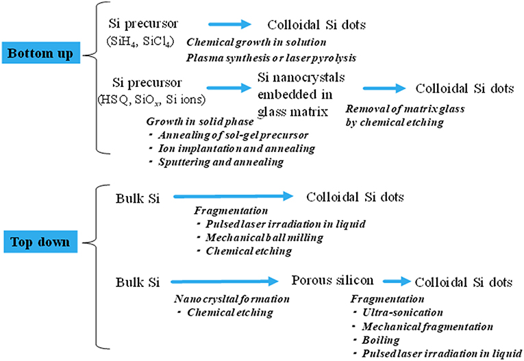
Figure 2. Summary of typical production processes for nc-Si dots. The bottom-up and top-down routes are shown in up and lower parts. Each process sequence represents arrows from left to right.
Another typical bottom-up process is laser pyrolysis (Ehbrecht et al., 1997; Ehbrecht and Huisken, 1999; Ledoux et al., 2002; Li et al., 2003, 2004; Hua et al., 2006) or plasma synthesis (Mangolini et al., 2005; Nozaki et al., 2007; Anthony and Kortshagen, 2009; Gupta et al., 2009; Shen et al., 2010; Miller et al., 2012; Askari et al., 2015) from the silicon precursor such as silane. In these methods, the treatment of a pulsed laser or an induction of high frequency power leads to the decomposition of precursor molecules and formation of Si clusters. Subsequently, the growth of the silicon nanoparticles occurs due to the aggregation of the generated clusters. The obtained nanoparticles consist of the single phase crystalline core and the surrounding amorphous layer of SiOx (Ledoux et al., 2002; Mangolini et al., 2005). Then, to adequately terminate the surfaces or further control the nanoparticle size, stain etching was performed in HF/HNO3 aqueous solution, where the oxidation of the silicon surface of the nanoparticles occurs and the removal of the oxide layer leads to the decrease in the size (Li et al., 2003; Gupta et al., 2009). Subsequent organic capping may also be formed by an additional chemical treatment (Li et al., 2004; Hua et al., 2006). Due to such size control processes by stain-etching, the PL emission colors of the formed nanoparticles were tuned in all visible spectral regions (Gupta et al., 2009). The emission color of the nanoparticles also changes from blue to green by the total pressure of the plasma reactor (Shen et al., 2010). In the case of the laser pyrolysis, an excellent size separation was demonstrated by using a molecular-beam chopper synchronization of the irradiation pulsed laser combining the time-of-flight mass spectroscopy (Ehbrecht et al., 1997; Ehbrecht and Huisken, 1999). Formation of such size-separated nc-Si dots reveals the clear size-dependent PL data in a red spectral region (Figure 3), and an excellent agreement between the theory and data was shown (Ledoux et al., 2002). Typical PL quantum efficiencies of the nanoparticles prepared by laser pyrolysis are 1–30% depending on their size, i.e., the larger (smaller) nanoparticles with a diameter of 8 nm (3.5 nm) have lower (higher) efficiencies (Ledoux et al., 2002).
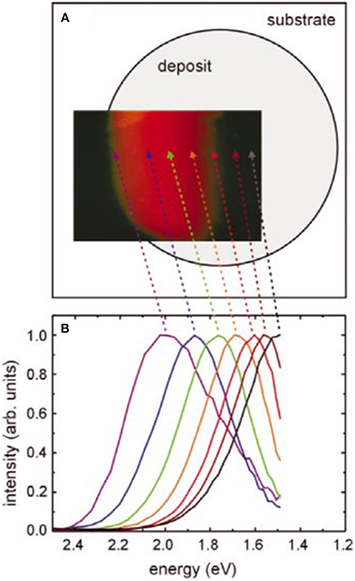
Figure 3. (A) Pictures of the size separated nc-Si dots prepared by laser pyrolysis and (B) corresponding PL spectra. Reprinted with permission from Ledoux et al. (2002), Copyright 2013 AIP Publishing.
Recently, a new type of bottom-up process using sol-gel precursors for the formation of the nc-Si dots has been developed by Veinot's Group (Hessel et al., 2006, 2008; Henderson et al., 2009; Clark et al., 2010; Kelly et al., 2010). After the annealing of hydrogen silsesquoxane (HSiO1.5) at high temperature (900–1400°C) under the H2/Ar atmosphere, nanocrystalline silicon forms in the oxide matrix (Hessel et al., 2006). With varying annealing temperature and/or annealing time, the size of the nanocrystals can be controlled. After the nanocrystal formation, HF treatment of the nanocrystal embedded oxide liberates the nanocrystals as a freestanding form due to the etched removal of the oxides, i.e., the formation of the hydrogen-terminated colloidal silicon nanoparticles. The various organic termination can be formed by the subsequent photo- or thermally-induced hydrosililation between the hydrogen surface of silicon nanoparticles and unsaturated organic species, which can make the colloidal nanoparticles soluble in desired types of solvents (Clark et al., 2010; Yu et al., 2013). The colloidal silicon nanoparticles prepared by this process exhibit usual quantum confinement induced size-dependent PL in the yellow to red region (Hessel et al., 2006). However, by attaching particular organic functional groups on the surface of the nanoparticles, the emission color can be tuned in all visible range (blue to red) without size control of dots, e.g., the diphenylamine functionalized dots shows the yellow emission (Dasog et al., 2014). These PL emission colors were independent on the polarity of the solvent and the excitation wavelength, indicating that the origin of the PL is the recombination at unknown surface states. The recombination lifetimes of such surface-related PL emission are much faster (several nanoseconds) than that of the usual quasi-direct electron-hole recombination due to quantum confinement effect. Note that their PL quantum efficiencies are 20–30% (Dasog et al., 2014). By using the silicon nanoparticles prepared by this sol-gel precursor process, solution-based multicolor light emitting diodes having high external quantum efficiencies ~1.1% were demonstrated (Figure 4) (Maier-Flaig et al., 2013) with combining the size separation technique (Mastronardi et al., 2011). Successful demonstration of such diode is thanks to the ease of the preparation handling and mass productivity as discussed below. Moreover, Ghosh et al. reported the improved sol-gel precursor process to form brighter silicon nanoparticles under mild condition, and fabricated white- (Ghosh et al., 2014) and red-emitting diodes (Ghosh et al., 2018). In addition to these sol-gel precursor process, the HF etching process of SiOx films incorporated in crystalline silicon nanoparticles, which is prepared by radio-frequency sputtering method (Shinoda et al., 2006; Sugimoto et al., 2012) and subsequent thermal annealing, provides the formation of the colloidal nc-Si dot.
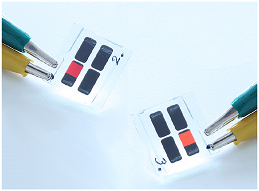
Figure 4. Photographs of the multicolor light emitting diodes utilizing the size-separated silicon nanocrystals prepared by the thermal process of the sol-gel precursor (hydrogen silsesquoxane). Reprinted with permission from Maier-Flaig et al. (2013), Copyright 2013 ACS Publishing.
Top-Down Fabrication Routes of Silicon Quantum Dot
One of the most simple top-down processes is the mechanical fragmentation of bulk silicon and/or silica by a ball milling technique (Lam et al., 2000; Heintz et al., 2007). In particular, Heintz et al. (2007) demonstrated the formation of blue-emitting quantum dots with alkyl-termination by combining the high energy ball milling of a bulk silicon chunk and a simultaneous chemical reaction with unsaturated organic species. Furthermore, chemically size reducing technique by stain-etching of bulk silicon or silicon rich oxide powders have been reported (Sato and Swihart, 2006; Sato et al., 2009; Goller et al., 2010). Sato et al. demonstrated the PL color tuning (green to red) of the quantum dots (2–3 nm) by stain-etching of the polycrystalline powder with an average diameter of 50 nm in HF/HNO3 aqueous solution with ultrasound treatment which allows uniform etching (Sato et al., 2009). Furthermore, Goller et al. reveal that spherical quantum dots (3–10 nm) formed by stain-etching of silicon powder (25 nm), and they show a single exponential PL decay curves (Goller et al., 2010), in contrast to stretched exponential curves for usual silicon nanocrystals including PS (Pavesi and Ceschini, 1993). This is considered to be attributed to a uniform spherical shape of the dots.
Laser ablation of bulk silicon in liquid, such as water (Švrček et al., 2006; Umezu et al., 2007), organic solvent (Shirahata et al., 2010; Abderrafi et al., 2011), and supercritical fluid (Saitow and Yamamura, 2009) is a simple fabrication route for the nc-Si dots. Umezu et al. demonstrated that the irradiation of pulsed laser light (532 nm, 10 mJ/cm2) to a bulk silicon wafer in hexane and water generates blue-emitting oxide-capped colloidal silicon nanoparticles (Umezu et al., 2007). Švrček et al. revealed that the size of the nanoparticles depends on the irradiation laser power in the diameter range from 2 to 10 nm, and higher power laser irradiation causes the fragmentation of the aggregated nanoparticles (Švrček et al., 2016). Shirahata et al. demonstrated the pulsed laser irradiation to a bulk silicon wafer in unsaturated organic solvents such as 1-octene yields organically-capped silicon nanoparticles (Shirahata et al., 2010). The nanoparticle formation mechanism in these laser ablation methods in liquid is as follows: Intense pulsed laser light ablates bulk silicon target, resulting in the formation of the silicon vapors and/or clusters. Then, the ablated silicon vapor condensed into the silicon nanoparticles at the liquid/vapor interface. In particular, using the unsaturated organic solvent, chemical reaction between the surface of the nanoparticles and unsaturated bonds of the organic solvent causes the efficient surface termination, resulting in a relatively higher PL quantum efficiency (~10%). However, in these pulsed laser ablation methods, the formed silicon nanoparticles have relatively larger size distribution and an exact size control are essentially difficult.
An important top-down process for nc-Si dots is the formation of the PS by electrochemical etching of silicon wafer and subsequent pulverization of the porous layer. As the porous layer consists of the assembly of nc-Si dots, a relatively mild pulverization treatment can render the porous layer free-standing nanoparticle form. Several pulverization techniques have been employed, such as ultra-sonification (Heinrich et al., 1992), and mechanical milling (Ryabchikov et al., 2012; Luna López et al., 2014). Heinrich et al. firstly demonstrated that the ultra-sonification of the PS layer in various solvents, such as methanol, toluene, and water, generates the colloidal silicon nanoparticles (Heinrich et al., 1992). However, the obtained colloidal nanoparticles have a wide size distribution from several nanometers to hundreds of nanometers. Thus, to purely obtain light emitting nanoparticles (a dimeter range from 2 to 10 nm) due to quantum confinement effect, additional size separation procedures are usually needed. For example, the subsequent filtering of the supernatant part of as-prepared colloidal solution was performed (Valenta et al., 2008). Furthermore, the additional chemical etching of the as-prepared colloidal nanoparticles was also employed to obtain colloidal samples having controllable visible PL emission from green to red (Choi et al., 2007; Kang et al., 2009). The surface of the obtained colloidal silicon nanoparticles prepared by this method are oxygen or hydrogen terminations. The silicon nanoparticles formed by the pulverization of the PS usually have the similar PL emission properties as original PS, although they exhibit a blue shift of the PL peak due to being free from matrix stress (Kusová et al., 2012) and the apparent increase in PL quantum yields (Credo et al., 1999). Organically capped nanoparticles can be also obtained by an additional chemical treatment, i.e., the photo-assisted hydrosilylation in organic solvent (Buriak, 2009). Kusová demonstrated the formation of yellow emitting organically capped nc-Si dots prepared by combining the sonification of porous layer and subsequent photo-assisted hydrosilylation treatments (Figure 5) (Kusová et al., 2010). Interestingly, these colloidal nanoparticles exhibit the nanosecond PL decay, due to electron-hole direct gap recombination induced by the crystalline strain and resultant modification of the electronic band structure (Kusová et al., 2014). Another simple process to pulverize the PS is boiling of the PS in an organic solvent with unsaturated bonding (Lie et al., 2002; Chao et al., 2007). This treatment leads to the formation of alkyl-capped silicon nanoparticles with a diameters of ~2.5 nm, resulting from the bubble formation by hydrosilylation between the unsaturated organic solvent and hydrogen-terminated silicon surface (Phatvej et al., 2018), and resultant pulverization of PS.
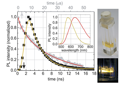
Figure 5. Yellow emitting nc-Si dots with nanosecond PL decay. Reprinted with permission from Kusová et al. (2010), Copyright 2010 ACS Publishing.
Efficient Approaches for the Silicon Quantum Dot Production
There are various criteria to evaluate the productivity for the nc-Si dot fabrication. Askari et al. summarized the figure of merit such as absolute throughput (kgh−1) and throughput density (kgh−1m−2), of above mentioned various processes (Askari et al., 2015). In this subsection, we summarize recent advances in the view of the production quantity per experimental batch. Zhong et al. produced ~10 g of green emitting green-quantum dots from ~100 g silicon precursor (C6H17NO3Si) by solution-phase chemical process for 30 min (Zhong et al., 2015). Here, we define the production yield as the ratio of the weight of the produced quantum dots to that of original silicon material. The production yield per batch of Zhong's process is ~10%. In the high annealing process of sol-gel precursor (~2 h per batch), typically 20 mg of the hydrogen terminated nc-Si dots were produced from 200 mg of HSQ silicon precursor, corresponding to the production yield of ~10% (Islam et al., 2017). Bose et al. demonstrated that the quantum dots can be prepared from the reduction of rice husk by rapid microwave heating (Bose et al., 2018). The production yield of this process is ~5%, i.e., 0.1 g of nanoparticles from 2 g of rice husk per batch. Note that the plasma synthesis from silane precursor provides ~20 mg quantum dots per batch (~45 min) with almost 100% of production yield, representing the complete conversion from the silane precursor (Mangolini et al., 2005). We summarize the production yields for these processes in Table 1.
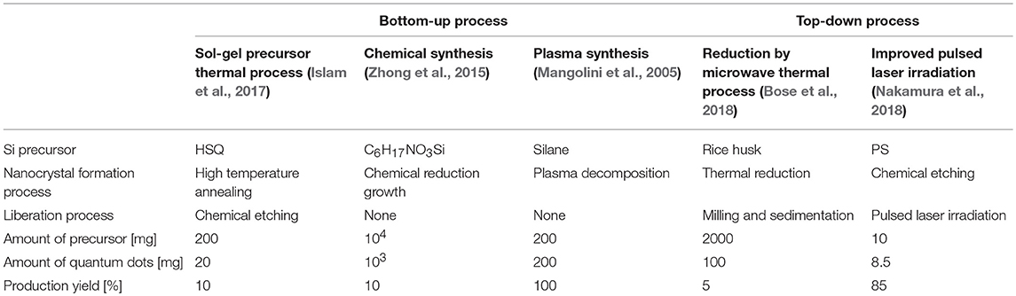
Table 1. Typical production yields of nc-Si dot per batch in various processes.
Very recently, Nakamura et al. demonstrated that the pulsed laser irradiation of the PS powder in organic solution efficiently generates the nc-Si dots and the formed quantum dots exhibited the multicolor PL emission in blue (Nakamura et al., 2014), white (Yuan et al., 2017a), and red (Nakamura et al., 2016; Yuan et al., 2017b) regions. The PL quantum efficiencies are much higher (~10–30%) than the original PS (~1%) (Nakamura et al., 2016). The prepared quantity of the quantum dots is more than ten times larger than the usual pulsed laser ablation method using the bulk silicon target (Nakamura et al., 2014). The formation mechanisms depend on laser irradiation conditions, i.e., the ablation of porous layer and subsequent condensation into nanoparticles, or the pulverization of the porous layer resulting from the laser induced thermal stress. In the case of the pulverization induced formation of the dots, the PL emission color was able to be controlled via etching condition of the target PS (Figure 6) (Nakamura et al., 2016), i.e., the changes in the size of nanocrystalline porous network core. As described in the above subsection, such PL emission color control was usually difficult in the usual laser ablation process using bulk silicon target. This efficient fabrication of the nc-Si dots is attributed to unique thermal properties of PS. The PS has a much smaller thermal conductivity (in the range of 0.5–1.0 W/mK), which is comparative to insulators such as quartz glass and rubber (Lysenko et al., 1999; Valalaki and Nassiopoulou, 2013, 2014, 2017; Koshida, 2017b). In addition to the conductivity, heat capacities are also very low (0.2–0.6 MJ/m3K) in contrast to the insulators (Koshida, 2017b). These unique thermal properties of PS cause a local heating inside the porous layer when the pulse laser irradiated to it, and the efficient ablation or fragmentation occurs. By improved pulsed laser irradiation process for 10 mg of PS, ~8.5 mg of red emitting nc-Si dots has been produced (Nakamura et al., 2018). This production amount of the quantum dot per batch is much larger than the boiling process of PS, i.e., several hundred micro grams of dots from 1 cm2 of silicon chip wafer (Dickinson et al., 2008; Alsharif et al., 2009). Moreover, the production yield of this process (~85%) is larger than the above mentioned chemical synthesis and high temperature annealing process of sol-gel precursor (Islam et al., 2017) (see Table 1). Thus, the demonstrated laser induced heating process of PS provides an energy- and cost-effective route for production of nc-Si dots.
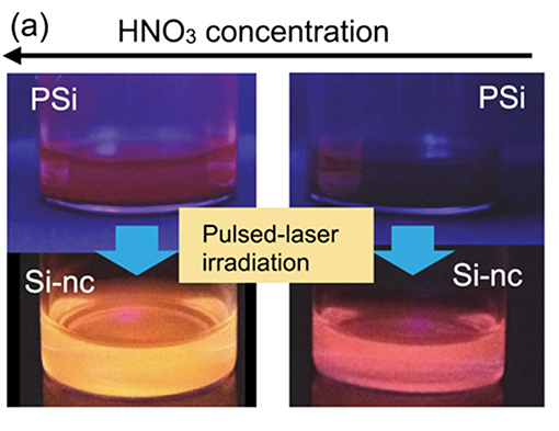
Figure 6. Pictures of multicolor PL emission from nc-Si dots produced by the pulsed laser irradiation to PS prepared by different etching conditions. Reprinted with permission from Nakamura et al. (2016), Copyright 2016 AIP Publishing.
Quasiballistic Electron Emission
Emission Mechanism and Characteristics
The device is composed of a thin film surface electrode, a PS layer (~1 μm thick), a silicon wafer substrate, and a back contact (Figure 7). As observed by transmission electron micrograph (TEM) shown in this figure, the PS layer prepared by galvano-static anodization and additional oxidation includes nc-Si dots (~3 nm in mean diameter) interconnected with tunnel oxides. In this PS layer, there is a multiple-tunneling transport mode through nc-Si dot chain, and quasiballistic hot electrons are efficiently generated (Mori et al., 2011). Under the condition that a positive voltage is applied to the surface electrode with respect to the substrate, electrons are accelerated in the PS layer toward the outer surface, and then some of them are emitted through the surface electrode. The emission starts at an onset voltage corresponding to the work function potential of the surface electrode. The applied voltage dependence of the emission current follows the Fowler-Nordheim tunneling scheme. The emission efficiency η, defined as the ratio of the emission current density to the diode current density, depends on the nanostructure arrangement of nc-Si dots, quality of interfacial tunneling oxide, and the surface electrode material.
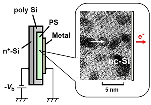
Figure 7. Schematic structure of PS-based quasiballistic electron emitter. A cross-sectional transmission electron microscopy (TEM) photograph of PS layer is also shown.
When a monolayer graphene is used as a surface electrode, the typical η value is drastically enhanced to 6.3% at an applied voltage of 10 V (Kojima et al., 2018a) due to a high transparency of monolayer graphene for quasiballistic electrons. At that applied voltage, the mean energy of output electrons becomes higher than 2 eV. The corresponding electron temperature is far from the thermal equilibrium. The mean energy of emitted electrons can be tuned well by the applied voltage while keeping narrow energy dispersion. Both the output electron energy distribution and the emission angle dispersion become significantly narrow even at room temperature. The energy distribution becomes more monochromatic at a low temperature of around 150 K. The measured emission angle dispersion is just ±8° with respect to the surface normal (Kojima et al., 2018b). The relatively low operation voltages and the compatibility with silicon planar processing make it possible to drive the emitter array under an active-matrix mode.
Applications of Quasiballistic Electron Source
(i) Availability for varied media
Being the energetic, directional, planar, and uniform emission, the quasiballistic emission from PS is insensitive to vacuum pressure, in contrast to the conventional cold cathodes such as field emitters and metal-insulator-metal ones. Far from it, the PS emitter operates in gases and even in solutions. The application studies have been carried out in vacuum (flat panel display, multibeam parallel lithography, high-sensitivity image sensor), in atmospheric pressure gases (negative ion generation, non-discharge VUV emission), and in solutions (H2 gas evolution, pH control, thin film deposition) (Koshida, 2017a). As specific approaches, two topics on the development that demonstrates the characteristic feature of the PS emitter are presented here.
(ii) Multibeam parallel lithography
In advanced silicon device technology, a high resolution (below 10 nm), high throughput, and cost-effective nanofabrication process is strongly required. Though electron beam (EB) is a very attractive exposure source from a viewpoint of the resolution, the conventional focused EB writer has a seriously limited throughput. If a practical multibeam exposure scheme could be possible, the usefulness of mask-less EB direct-write should be dramatically enhanced. Its major possible applications are photomask fabrication and mask-less direct-write exposure. Specifications of multibeam parallel lithography systems under development are summarized in Table 2.
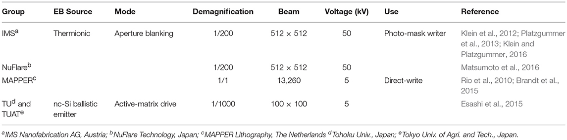
Table 2. Developing studies of multibeam parallel EB lithography.
In the conventional systems, thermionic emitter or thermally assisted field emitter is used as an electron source. Since the employment of active-matrix drive is difficult in that case, broadened electron beam is spatially switched by aperture blanking method for generating multibeam (Rio et al., 2010; Klein et al., 2012; Platzgummer et al., 2013; Brandt et al., 2015; Klein and Platzgummer, 2016; Matsumoto et al., 2016). In contrast, the PS approach is characterized by active-matrix drive of arrayed emitters (Esashi et al., 2015). The PS emitter array can be fabricated on a Si-wafer substrate by planar processes. The back contact of each electron emitter with an active area of 10 × 10 μm2 is interconnected to an active matrix driving circuit using a through-silicon-via (TSV) technique (Figure 8A). A CMOS-based LSI circuit has been developed for the multibeam (100 × 100) parallel lithography.
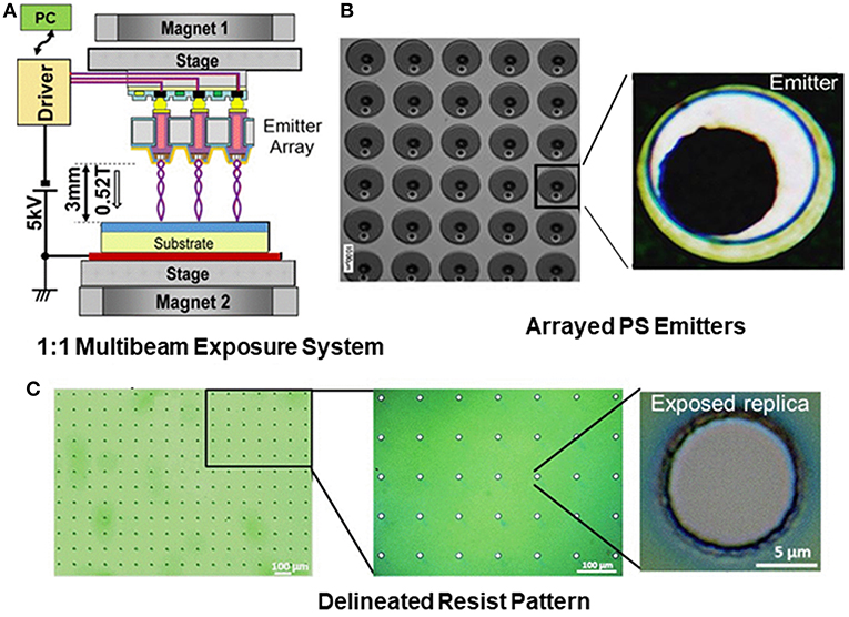
Figure 8. (A) Schematic configuration of 1:1 electron multibeam exposure system using arrayed nanocrystalline PS emitters. (B) SEM photographs of emitter array. The emission area is 12 μm in diameter in this case. (C) Delineated resist patterns.
The compatibility of the implemented LSI with the active-matrix operation was confirmed, including the basic function for the electron emitter process variation compensation and the test of integrated devices. The evaluation was performed with the 1:1 exposure test system, in which an EB-resist coated target wafer was placed at about 3 mm distance from the emitter surface (Figure 8B) and the exposed resist pattern is shown in Figure 8C. It has been demonstrated that the integrated nc-Si emitter array is compatible with the active-matrix drive for multi-beam massive parallel exposure, and that the selected emitter pattern is delineated corresponding to the activated emitters. In accordance with the results of beam optics simulation in the prototype system, the miniaturized electron optics is suitable for 10 nm order EB writing. For the practical use with a throughput comparable to extreme ultra-violet (EUV) lithography, criteria of the electron beam number and the resolution target to be pursued are 106 beams and 5 nm, respectively.
(iii) Reductive deposition of thin films
From a chemical viewpoint, the PS emitter can be regarded as a supplier of electrons with highly reducing activity. Its direct application is liquid-phase thin film deposition of metals and semiconductors under an electron incident mode (Suda et al., 2016). The deposition process is illustrated in Figure 9. Output of quasiballistic electrons of the nc-Si emitter impinges onto the target substrate on which an extremely small amount of salt solutions such as CuCl2, SiCl4, and GeCl4 was coated in advance with a thickness of 100 nm. The spacing between the emitter and substrate was controlled in the range from 500 nm to 100 μm by a piezoelectric actuator, taking the relation between the electron mean free path and the vacuum pressure of used solution into account. The experiments were done in a N2-gas filled glove box.
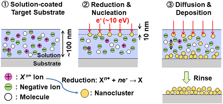
Figure 9. Process of liquid-phase reductive thin-film deposition promoted by direct incidence of quasiballistic electrons emitted from nanocrystalline PS cold cathode.
After the emitter operation for a few minutes, residual solutions were removed, and then thin Cu, Si, and Ge films are formed on the incident area as shown in Figure 10. According to the structure and compositional characterizations of deposited thin films, every film consists of nanoclusters. No contaminations were detected by X-ray photoelectron spectroscopy (XPS). Obviously thin films are deposited with no byproducts. Thin films can be deposited at room temperature on varied substrates including insulating layers (i.e., oxidized c-Si wafer) and flexible polymers. In addition, a mixture solution such as SiCl4+GeCl4 is available for deposition of thin SiGe films with a controllable composition.
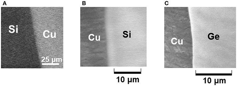
Figure 10. SEM photographs of deposited thin films of Cu (A), Si (B), and Ge (C).
Incident electrons with energy of 10 eV can penetrate 10 nm deep in solutions (Emfietzoglou et al., 2009), and reduce positive ions therein followed by the formation of nanoclusters and deposition. Thermodynamic investigation supports that the incident electron energy meets the requirement for preferential nucleation of atoms rather than their out-diffusion (Suda et al., 2017). The theoretical analysis based on the reaction diffusion equation suggests that the deposition rate depends mainly on the incident electron current density Je, and that it reaches a stationary value within 0.1 s after electron incidence (Suda et al., 2018). At the typical condition of Je = 10–100 μA/cm2, the estimated stationary deposition rate of Cu, Si, and Ge films are around 0.2–2.0 nm/min. This is consistent with the experimental results.
Typical thin film deposition techniques are summarized in Table 3. The most widely used dry processes (chemical and physical vapor deposition) are established by precise control of temperature, vacuum pressure, and gas flow rate (Seshan, 2012). The wet electroplating, based on exchange of thermalized electrons at the working and counter electrodes, proceeds at room temperature with gas evolutions. It is mainly used to deposit thin metal films (Schlesinger and Paunovic, 2010). Electron-beam-induced deposition (EBID), on the other hand, has been studied to form cluster, metal nanowires, thin films, and nanostructures (Kiyohara et al., 2002; Adelung et al., 2004; Gazzadi and Frabboni, 2005; van Dorp et al., 2005; Randolph et al., 2006; Frabboni et al., 2008; Furuya, 2008; van Dorp and Hagen, 2008; Botman et al., 2009; de Boer et al., 2011; Vollnhals et al., 2013; den Heijer et al., 2014; Leenheer et al., 2015). The focused electron beam with high-energies of 10–50 keV in the conventional scanning or transmission electron microscope is transmitted through membranes and then hits the absorbed gases or ionic liquids on the substrate leading to decomposition of molecules. The key issue is to reduce carbon and other contaminations in deposited thin films. The ballistic electron incidence mode mentioned above is based on the mechanism different from EBID. Unilateral reduction proceeds with neither gas evolution nor by-product generation. In addition, the deposition of thin metal and group IV semiconductor films is available for varied substrates.
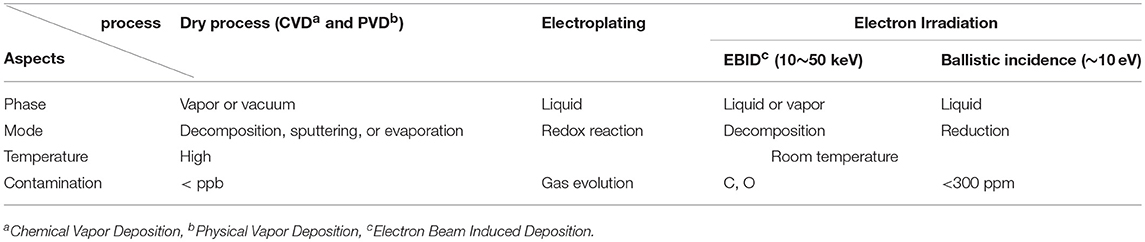
Table 3. Comparative survey of thin film deposition processes.
Thermo-Acoustic Emission and Applications
The PS acoustic devices are composed of a thin-film surface heater electrode, a PS layer, and a c-Si wafer. Due to a strong phonon confinement and interfacial scattering in PS, the thermal conductivity of PS layers, α, is drastically lowered in comparison to that of bulk silicon (Lysenko et al., 1999; Valalaki and Nassiopoulou, 2013, 2014, 2017; Koshida, 2017b). At the same time, its volumetric heat capacity C is also significantly decreased. In the case of high-porosity PS, particularly, both α and C values become close to the lower limit of solid state materials. Thus, the thermal diffusivity is extremely decreased. When a temperature fluctuation is produced by electrical input to the heater electrode, a significant acoustic wave is generated near the surface, because the thermos-acoustic transfer effect is inversely proportional to (Shinoda et al., 1999). A significant sound pressure amplitude is produced without any mechanical vibrations.
Due to the sound emission from still surface, the frequency response covering a fully wide range is free from the mechanical resonance. The theoretical limit of frequency response is 1 GHz. No resonant peaks are observed in the whole range of available frequency. The broad-band flat emissivity of the PS device is useful for reproducing complicated ultrasonic communication calls and male-female interactions between mice (Kihara et al., 2006; Uematsu et al., 2007). Conventional ultrasound emitters cannot be utilized for this application because of a resonant frequency response and a bulky size larger than mice. As previously demonstrated, mouse mothers were attracted by pup ultrasonic vocalizations (USVs) reproduced by an nc-Si emitter, while they did not respond to other synthesized sounds. It was also found that the response to pup USVs was enhanced by social experiences (Okabe et al., 2013). Recent study on mutual recognition between mother and infant suggests that pup USVs looks to have an individual signature used in pup differentiation by mouse mothers, similar to acoustic communication between human mothers and their infants (Asaba et al., 2015; Mogi et al., 2017).
Regarding thin metal film heaters and underlying thermal insulators, many studies have been conducted by using varied combinations: suspended Al wires-air (Niskanen et al., 2009), Si nanowires-polymer or -glass (Tian et al., 2011a), indium-tin-oxide film-glass (Daschewski et al., 2015), Si nanoparticles-sapphire (Odagawa et al., 2010), conducting polymers-glass (Tian et al., 2011b), thin Au film-porous polymer (Chitnis et al., 2012), thin Ag–Pd film-glass-Al2O3 (Nishioka et al., 2015), carbon nanotube (CNT)-air (Xiao et al., 2011), or -grooved Si (Wei et al., 2013), graphene-polymer (Suk et al., 2012; Tian et al., 2014; Kim et al., 2016; Tao et al., 2016; Sbrockey et al., 2018), -porous Al2O3 (Tian et al., 2012), or -glass (Fei et al., 2015), CNT-laser-scribed graphene-polymer (Yeklangi et al., 2018), and W-Al2O3-polymer (Brown et al., 2016). The basic characteristics of these devices are consistent with the theoretical analyses of the thermo-acoustic effect and its key factors (Hu et al., 2010, 2012a,b, 2014; Vesterinen et al., 2010; Daschewski et al., 2013; Lim et al., 2013; Yang and Liu, 2013; Wang et al., 2015; Tong et al., 2017; Xing et al., 2017). Making use of the non-resonant and broad-band emissivity with no harmonic distortions, possible applications have been pursued to audible compact speaker under a full digital drive, probing source for 3-dimentional object sensing in air, acoustic pressure generator for noncontact actuation, directivity control under phased array configuration, loud speaker, noise cancellation, thermoacoustic tomography, and thermoacoustic sound projector (Koshida, 2017c; Aliev et al., 2018; Bobinger et al., 2018; Julius et al., 2018; Liu et al., 2018; Song et al., 2018).
Summary
Including photonic visible luminescence, emerging functions of nanostructured PS has extended to electronics, biometrics, biomedicine, acoustics, thermology, and energetics. In the quantum-size silicon, especially, the emissive properties of photons, electrons, and sound are activated. From a technological viewpoint, cost- and power-effective production of luminescent nc-Si powder or colloid is desired for wide applications. As one practical approach, high-yield fabrication of strongly luminescent colloidal nc-Si dots has been developed by employing in-situ self-regulated process for pulverization of anodized PS by pulsed laser irradiation. A multiplier tunneling transport through nc-Si dots, on the other hand, induces quasiballistic electron emission. The potential of nc-Si cold cathode has been made clear by using monolayer graphene as a surface electrode. This makes the foundation more solid for applications to massively parallel EB lithography under an active-matrix drive and to reductive thin film deposition of metals and semiconductors. Based on specific thermal properties of PS, on the other hand, thermos-acoustic device has been developed. Observed broad-band non-resonant sound emission from a compact PS device provides standard ultrasound source for researches in the bio-acoustic communications. These studies meet in the direction and requirements for diversification of silicon technology.
Author Contributions
NK: overview, ballistic electron emission, thermo-acoustic device. TN: visible luminescent Si quantum dots.
Conflict of Interest Statement
The authors declare that the research was conducted in the absence of any commercial or financial relationships that could be construed as a potential conflict of interest.
Acknowledgments
The author NK would like to thank Prof. M. Esashi, Prof. K. Kikusui, Dr. A. Kojima, and Dr. R. Suda for their support and cooperation. This work was partially supported by the Formation of Innovation Centers for Fusion of Advanced Technologies programs setup by MEXT, Japan.
Footnotes
1. ^IRDS. IEEE International Roadmap for Devices and Systems (IRDS). Available online at: https://irds.ieee.org
References
Abderrafi, K., Calzada, R. G., Gongalsky, M. B., Suárez, I., Abarques, R., Chirvony, V. S., et al. (2011). Silicon nanocrystals produced by nanosecond laser ablation in an organic liquid. J. Phys. Chem. C 115, 5147–5151. doi: 10.1021/jp109400v
Adelung, R., Ernst, F., Zheng, N., and Landau, U. (2004). In situ nanoscale observation and control of electron-beam-induced cluster formation. J. Vac. Sci. Technol. B 22, 1797–1802. doi: 10.1116/1.1767830
Aliev, A. E., Codoluto, D., Baughman, R. H., Ovalle-Robles, R., Inoue, K., Romanov, S. A., et al. (2018). Thermoacoustic sound projector: exceeding the fundamental efficiency of carbon nanotubes. Nanotech 29:325704. doi: 10.1088/1361-6528/aac509
Alsharif, N. H., Berger, C. E., Varanasi, S. S., Chao, Y., Horrocks, B. R., and Datta, H. K. (2009). Alkyl-capped silicon nanocrystals lack cytotoxicity and have enhanced intracellular accumulation in malignant cells via cholesterol-dependent endocytosis. Small 5, 221–228. doi: 10.1002/smll.200800903
Anthony, R., and Kortshagen, U. (2009). Photoluminescence quantum yields of amorphous and crystalline silicon nanoparticles. Phys. Rev. B 80:115407. doi: 10.1103/PhysRevB.80.115407
Asaba, A., Okabe, S., and Nagasawa, M. (2015). Determining ultrasonic vocalization preferences in mice using a two-choice playback test. J. Vis. Exp. 103:e53074/1-8. doi: 10.3791/53074
Askari, S., Macias-Montero, M., Velusamy, T., Maguire, P., Svrcek, V., and Mariotti, D. (2015). Silicon-based quantum dots: synthesis, surface and composition tuning with atmospheric pressure plasmas. J. Phys. D: Appl. Phys. 48:314002. doi: 10.1088/0022-3727/48/31/314002
Bobinger, M., La Torraca, P., Mock, J., Becherer, M., Cattani, L., Angeli, D., et al. (2018). Solution-processing of copper nanowires for transparent heaters and thermo-acoustic loudspeakers. IEEE Trans. Nanotech. 17, 940–947. doi: 10.1109/TNANO.2018.2829547
Bose, S., Ganayee, M. A., Mondal, B., Baidya, A., Chennu, S., Mohanty, J. S., et al. (2018). Synthesis of silicon nanoparticles from rice husk and their use as sustainable fluorophores for white light emission. ACS Sust. Chem. Eng. 6, 6203–6210. doi: 10.1021/acssuschemeng.7b04911
Botman, A., Hagen, C. W., Li, J., Thiel, B. L., Dunn, K. A., Mulders, J. J. L., et al. (2009). Electron postgrowth irradiation of platinum-containing nanostructures grown by electron-beam-induced deposition from Pt(PF3)4. J. Vac. Sci. Technol. B 27:2759. doi: 10.1116/1.3253551
Brandt, P., Tranquillin, C., Wieland, M., Bayle, S., Milléquant, M., and Renault, G. (2015). Alternative stitching method for massively parallel e-beam lithography. Proc SPIE 9423:942312. doi: 10.1117/1.JMM.14.3.031203
Brown, J. J., Moore, N. C., Supekar, O. D., Gertsch, J. C., and Bright, V. M. (2016). Ultrathin thermoacoustic nanobridge loudspeakers from ALD on polyimide. Nanotechnol. 27:475504. doi: 10.1088/0957-4484/27/47/475504
Buriak, J. M. (2009). Organometallic chemistry on silicon and germanium surfaces. Chem. Rev. 102, 1271–1308. doi: 10.1021/cr000064s
Canham, L. (1990). Silicon quantum wire array fabrication by electrochemical and chemical dissolution of wafers. Appl. Phys. Lett. 57:1046. doi: 10.1063/1.103561
Canham, L. (1995). Bioactive silicon structure fabrication through nanoetching techniques. Adv. Mater. 7, 1033–1037. doi: 10.1002/adma.19950071215
Chao, Y., Siller, L., Krishnamurthy, S., Coxon, P. R., Bangert, U., Gass, M., et al. (2007). Evaporation and deposition of alkyl-capped silicon nanocrystals in ultrahigh vacuum. Nat. Nano. 2, 486–489. doi: 10.1038/nnano.2007.224
Cheng, X., Hinde, E., Owen, D. M., Lowe, S. B., Reece, P. J., Gaus, K., et al. (2015). Enhancing quantum dots for bioimaging using advanced surface chemistry and advanced optical microscopy: application to silicon quantum dots (SiQDs). Adv. Matter. 27, 6144–6150. doi: 10.1002/adma.201503223
Cheng, X., Lowe, S. B., Reece, P. J., and Gooding, J. J. (2014). Colloidal silicon quantum dots: from preparation to the modification of self-assembled monolayers (SAMs) for bio-applications. Chem. Soc. Rev. 43, 2680–2700. doi: 10.1039/C3CS60353A
Chitnis, G., Kim, A., Song, S. H., Jessop, A. M., Bolton, J. S., and Ziaie, B. (2012). A thermophone on porous polymeric substrate. Appl. Phys. Lett. 101:021911. doi: 10.1063/1.4737005
Choi, J., Wang, N. S., and Reipa, V. (2007). Photoassisted tuning of silicon nanocrystal photoluminescence. Langmuir 23, 3388–3394. doi: 10.1021/la062906+
Choi, M. K., Yang, J., Hyeon, T., and Kim, D.-H. (2018). Flexible quantum dot light-emitting diodes for next-generation displays. NPJ Flex. Electron. 2:10. doi: 10.1038/s41528-018-0023-3.
Clark, R. J., Dang, M. K., and Veinot, J. G. (2010). Exploration of organic acid chain length on water-soluble silicon quantum dot surfaces. Langmuir 26, 15657–15664. doi: 10.1021/la102983c
Coffinier, Y., and Boukherroub, R. (2016). “Surface chemistry of porous silicon,” in Porous Silicon: From Formation to Application, Vol. 1, eds. G. Korotcenkov (Boca Raton, FL: Taylor and Francis Group, CRC Press), 357–390.
Credo, G. M., Mason, M. D., and Burattoa, S. K. (1999). External quantum efficiency of single porous silicon nanoparticles. Appl. Phys. Lett. 74, 1978–1980. doi: 10.1063/1.123719
Daschewski, M., Boehm, R., Prager, J., Kreutzbruck, M., and Harrer, A. (2013). Physics of thermo-acoustic sound generation. J. Appl. Phys. 114:114903. doi: 10.1063/1.4821121
Daschewski, M., Kreutzbruck, M., and Prager, J. (2015). Influence of thermodynamic properties of a thermo-acoustic emitter on the efficiency of thermal airborne ultrasound generation. Ultrasonics 6, 16–22. doi: 10.1016/j.ultras.2015.06.008
Dasog, M., De los Reyes, G. B., Titova, L. V., Hegmann, F. A., and Veinot, J. G. (2014). Size vs surface: tuning the photoluminescence of freestanding silicon nanocrystals across the visible spectrum via surface groups. ACS Nano 8, 9636–9648. doi: 10.1021/nn504109a
de Boer, S. K., van Dorp, W. F., and De Hosson, J. T. M. (2011). Charging effects during focused electron beam induced deposition of silicon oxide. J. Vac. Sci. Technol. B 29:06FD01. doi: 10.1116/1.3659713
Debenedetti, W. J. I., Chiu, C., Sheng-Kuei, C., Radlinger, C. M., Ellison, R. J., Manhat, B. A., et al. (2015). Conversion from red to blue photoluminescence in alcohol Dispersions of alkyl-capped silicon nanoparticles: insight into the origins of visible photoluminescence in colloidal nanocrystalline silicon. J. Phys. Chem. C 119, 9595–9608. doi: 10.1021/acs.jpcc.5b01137
den Heijer, M., Shao, I., Radisic, A., Reuter, M. C., and Ross, F. M. (2014). Patterned electrochemical deposition of copper using an electron beam. Appl. Phys. Lett. Mater. 2:022101. doi: 10.1063/1.4863596
Dickinson, F. M., Alsop, T. A., Al-Sharif, N., Berger, C. E., Datta, H. K., Siller, L., et al. (2008). Dispersions of alkyl-capped silicon nanocrystals in aqueous media: photoluminescence and ageing. Analyst 133, 1573–1580. doi: 10.1039/b801921e
Dohnalová, K., Fucíková, A., Umesh, C. P., Humpolícková, J., Paulusse, J. M., Valenta, J., et al. (2012). Microscopic origin of the fast blue-green luminescence of chemically synthesized non-oxidized silicon quantum dots. Small 8, 3185–3191. doi: 10.1002/smll.201200477
Dohnalová, K., Gregorkiewicz, T., and Kusová, K. (2014). Silicon quantum dots: surface matters. J. Phys. Condens. Matter 26:173201. doi: 10.1088/0953-8984/26/17/173201
Dohnalová, K., Poddubny, A. N., Prokofiev, A. A. D. A. M., de Boer, W., Umesh, C. P., et al. (2013). Surface brightens up Si quantum dots: direct bandgap-like size-tunable emission. Light Sci. Appl. 2:e47. doi: 10.1038/lsa.2013.3
Ehbrecht, M., and Huisken, F. (1999). Gas-phase characterization of silicon nanoclusters produced by laser pyrolysis of silane. Phys. Rev. B 39, 2975–2985. doi: 10.1103/PhysRevB.59.2975
Ehbrecht, M., Kohn, B., Huisken, F., Laguna, M. A., and Paillard, V. (1997). Photoluminescence and resonant Raman spectra of silicon films produced by size-selected cluster beam deposition. Phys. Rev. B 56, 6958–6964. doi: 10.1103/PhysRevB.56.6958
Emfietzoglou, D., Kyriakou, I., Abril, I., Garcia-Molina, R., Petsalakis, I. D., Nikjoo, H., et al. (2009). Electron inelastic mean free paths in biological matter based on dielectric theory and local-field corrections. Nucl. Inst. Methods Phys. Res. B 267, 45–52. doi: 10.1016/j.nimb.2008.11.008
English, D. S., Pell, L. E., Yu, Z., Barbara, P. F., and Korgel, B. A. (2002). Size tunable visible luminescence from individual organic monolayer stabilized silicon nanocrystal quantum dots. Nano Lett. 2, 681–685. doi: 10.1021/nl025538c
Esashi, M., Kojima, A., Ikegami, N., Miyaguchi, H., and Koshida, N. (2015). Development of massively parallel electron beam direct write lithography using active-matrix nanocrystalline-silicon electron emitter arrays. Microsyst. Nanoeng. 1:15029. doi: 10.1038/micronano.2015.29
Fei, W., Zhou, J., and Guo, W. (2015). Low-voltage driven graphene foam thermoacoustic speaker. Small 11, 2252–2256. doi: 10.1002/smll.201402982
Frabboni, S., Gazzadi, G. C., Felisari, L., and Spessot, A. (2008). Fabrication by electron beam induced deposition and transmission electron microscopic characterization of sub-10-nm freestanding Pt nanowires. Appl. Phys. Lett. 88:213116. doi: 10.1063/1.2206996
Furuya, K. (2008). Nanofabrication by advanced electron microscopy using intense and focused beam. Sci. Technol. Adv. Mater. 9:014110. doi: 10.1088/1468-6996/9/1/014110
Gazzadi, G. C., and Frabboni, S. (2005). Fabrication of 5 nm gap pillar electrodes by electron-beam Pt deposition. J. Vac. Sci. Technol. B 23:L1. doi: 10.1116/1.1872015
Ghosh, B., Hamaoka, T., Nemoto, Y., Takeguchi, M., and Shirahata, N. (2018). Impact of anchoring monolayers on the enhancement of radiative recombination in light-emitting diodes based on silicon nanocrystals. J. Phys. Chem. C 122, 6422–6430. doi: 10.1021/acs.jpcc.7b12812
Ghosh, B., Masuda, Y., Wakayama, Y., Imanaka, Y., Inoue, J., Hashi, K., et al. (2014). Hybrid white light emitting diode based on silicon nanocrystals. Adv. Func. Mater. 24, 7151–7160. doi: 10.1002/adfm.201401795
Goller, B., Polisski, S., Wiggers, H., and Kovalev, D. (2010). Freestanding spherical silicon nanocrystals: a model system for studying confined excitons. Appl. Phys. Lett. 97:041110. doi: 10.1063/1.3470103
Gupta, A., Swihart, M. T., and Wiggers, H. (2009). Luminescent colloidal dispersion of silicon quantum dots from microwave plasma synthesis: exploring the photoluminescence behavior across the visible spectrum. Adv. Func. Mater. 19, 696–703. doi: 10.1002/adfm.200801548
Heath, J. R. (1992). A liquid-solution-phase synthesis of crystalline silicon. Science 258:1131. doi: 10.1126/science.258.5085.1131
Heinrich, J. L., Curtis, C. L., Credo, G. M., Sailor, M. J., and Kavanagh, K. L. (1992). Luminescent colloidal silicon suspensions from porous silicon. Science 255, 66–68. doi: 10.1126/science.255.5040.66
Heintz, A. S., Fink, M. J., and Mitchell, B. S. (2007). Mechanochemical synthesis of blue luminescent alkyl/alkenyl-passivated silicon nanoparticles. Adv. Mater. 19, 3984–3988. doi: 10.1002/adma.200602752
Henderson, E. J., Kelly, J. A., and Veinot, J. G. C. (2009). Influence of HSiO1.5 Sol–gel polymer structure and composition on the size and luminescent properties of silicon nanocrystals. Chem. Matter. 21, 5426–5434. doi: 10.1021/cm902028q
Hessel, C. M., Henderson, E. J., Kelly, J. A., Cavell, R. G., Sham, T.-K., and Veinot, J. G. C. (2008). Origin of luminescence from silicon nanocrystals: a near edge X-ray absorption fine structure (NEXAFS) and X-ray excited optical luminescence (XEOL) study of oxide-embedded and free-standing systems. J. Phys. Chem. C 112, 14247–14254. doi: 10.1021/jp802095j
Hessel, C. M., Henderson, E. J., and Veinot, J. G. C. (2006). Hydrogen silsesquioxane: a molecular precursor for nanocrystalline Si–SiO2 composites and freestanding hydride-surface-terminated silicon nanoparticles. Chem. Mater. 18, 6193–6146. doi: 10.1021/cm0602803
Holmes, J. D., Ziegler, K. J., Doty, R. C., Pell, L. E., Johnston, K. P., and Korgel, B. A. (2001). Highly luminescent silicon nanocrystals with discrete optical transitions. J. Am. Chem. Soc. 123, 3743–3748. doi: 10.1021/ja002956f
Hu, H., Wang, D., and Wang, Z. (2014). Solution for acoustic field of thermo-acoustic emission from arbitrary source. AIP Adv. 4:107114. doi: 10.1063/1.4898149
Hu, H., Wang, Y., and Wang, Z. (2012a). Wide band flat frequency response of thermo-acoustic emission. J. Phys. D: Appl. Phys. 45:345401. doi: 10.1088/0022-3727/45/34/345401
Hu, H., Wang, Z., Wu, H., and Wang, Y. (2012b). Analysis of spherical thermo-acoustic radiation in gas. AIP Adv. 2:032106. doi: 10.1063/1.4738497
Hu, H., Zhu, T., and Xu, J. (2010). Model for thermoacoustic emission from solids. Appl. Phys. Lett. 96:214101. doi: 10.1063/1.3435429
Hua, F., Erogbogbo, F., Swihart, M. T., and Ruckenstein, E. (2006). Organically capped silicon nanoparticles with blue photoluminescence prepared by hydrosilylation followed by oxidation. Langmuir 22, 4363–4370. doi: 10.1021/la0529106
Islam, M. A., Mobarok, M. H., Sinelnikov, R., Purkait, T. K., and Veinot, J. G. C. (2017). Phosphorus pentachloride initiated functionalization of silicon nanocrystals. Langmuir 33, 8766–8773. doi: 10.1021/acs.langmuir.7b00518
Julius, S., Gold, R., Kleiman, A., Leizeronok, B., and Cukurel, B. (2018). Modeling and experimental demonstration of heat flux driven noise cancellation on source boundary. J. Sound Vib. 434, 442–455. doi: 10.1016/j.jsv.2018.02.007
Jurbergs, D., Rogojina, E., Mangolini, L., and Kortshagena, U. (2006). Silicon nanocrystals with ensemble quantum yields exceeding 60%. Appl. Phys. Lett. 88:233116. doi: 10.1063/1.2210788
Kang, Z., Liu, Y., Tsang, C. H. A., Ma, D. D. D., Fan, X., Wong, N. B., et al. (2009). Water-soluble silicon quantum dots with wavelength-tunable photoluminescence. Adv. Mater. 6, 661–664. doi: 10.1002/adma.200801642
Kelly, J. A., Henderson, E. J., and Veinot, J. G. (2010). Sol–gel precursors for group 14 nanocrystals. Chem. Comm. 46:8704. doi: 10.1039/c0cc02609c
Kihara, T., Harada, T., Kato, M., Nakano, K., Murakami, O., Kikusui, T., et al. (2006). Reproduction of mouse-pup ultrasonic vocalizations by nanocrystalline silicon thermoacoustic emitter. Appl. Phys. Lett. 88:043902. doi: 10.1063/1.2168498
Kim, C. S., Hong, S. K., Lee, J. M., Kang, D. S., Cho, B. J., and Choi, J. W. (2016). Free-standing graphene thermophone on a polymer-mesh substrate. Small 12, 185–189. doi: 10.1002/smll.201501673
Kiyohara, S., Takamatsu, H., and Mori, K. (2002). Microfabrication of diamond films by localized electron beam chemical vapour deposition. Semicond. Sci. Technol. 17, 1096–1100. doi: 10.1088/0268-1242/17/10/311
Klein, C., Loeschner, H., and Platzgummer, E. (2012). 50 keV electron multibeam mask writer for the 11 nm HP node: first results of the proof of concept tool (eMET POC). Proc SPIE 8323:8323. doi: 10.1117/12.916613
Klein, C., and Platzgummer, E. (2016). “MBMW-101: World's 1st high-throughput multi-beam mask writer,” in Proceedings SPIE 9985, Photomask Technology (Bellingham, WA). doi: 10.1117/12.2243638
Kojima, A., Suda, R., and Koshida, N. (2018a). Improved quasiballistic electron emission from a nanocrystalline Si cold cathode with a monolayer-graphene surface electrode. Appl. Phys. Lett. 112:133102. doi: 10.1063/1.5017770
Kojima, A., Suda, R., and Koshida, N. (2018b). “Reduced energy-angle dispersion of output electrons from a nanocrystalline Si emitter with a monolayer-graphene surface electrode,” Technical Digest of 31st Int. Vacuum Nanoelectronics Conference. (2018, Kyoto), 38–39.
Koshida, N. (2017a). “Porous silicon ballistic hot electron emitter,” in Handbook of Porous Silicon, 2nd Edn., eds. L. Canham (New York, NY: Springer), 11.
Koshida, N. (2017b). “Thermal properties of porous silicon,” in Handbook of Porous Silicon, 2nd Edn, eds. L. Canham (New York, NY: Springer), 9.
Koshida, N. (2017c). “Porous silicon acoustic devices,” in Handbook of Porous Silicon, 2nd Edn, eds. L. Canham (New York, NY: Springer), 9.
Koshida, N., Kiuchi, Y., and Yoshimura, S. (1991). Photoconduction effects of porous Si in the visible region. Proceedings in Conference Photoelectrics Image Devices. London, Sep. 1991, 377–384.
Koshida, N., and Koyama, H. (1992). Visible electroluminescence from porous silicon. Appl. Phys. Lett. 60, 347–349. doi: 10.1063/1.106652
Koshida, N., Nagasu, M., Sakusabe, T., and Kiuchi, Y. (1985). The current-voltage characteristics of a photoelectrochemical cell using p-type porous-Si. J. Electrochem. Soc. 132, 346–349. doi: 10.1149/1.2113835
Koshida, N., Sheng, X., and Komoda, T. (1999). Quasiballistic electron emission from porous silicon diodes. Appl. Surf. Sci. 146, 371–376. doi: 10.1016/S0169-4332(99)00004-5
Kouassi, S., Gautier, G., Thery, J., Desplobain, S., Borella, M., Ventura, L., et al. (2012). Proton exchange membrane micro fuel cells on 3D porous silicon gas diffusion layers. J. Power Sources 216, 15–21. doi: 10.1016/j.jpowsour.2012.05.046
Kusová, K., Cibulka, O., Dohnalová, K., Pelant, I., Valenta, J., Fucíková, A., et al. (2010). Brightly luminescent organically capped silicon nanocrystals fabricated at room temperature and atmospheric pressure. ACS Nano 4, 4495–4504. doi: 10.1021/nn1005182
Kusová, K., Hapala, P., Valenta, J., Jelínek, P., Cibulka, O., Ondič, L., et al. (2014). Direct bandgap silicon: tensile-strained silicon nanocrystals. Adv. Mater. Inter. 1:1300042. doi: 10.1002/admi.201300042
Kusová, K., Ondič, L., Klimešová, E., Herynková, K., Pelant, I., Daniš, S., et al. (2012). Luminescence of free-standing versus matrix-embedded oxide-passivated silicon nanocrystals: the role of matrix-induced strain. Appl. Phys. Lett. 101:143101. doi: 10.1063/1.4756696
Lam, C., Zhang, Y. F., Tang, Y. H., Lee, C. S., Bello, I., and Lee, S. T. (2000). Large-scale synthesis of ultrafine Si nanoparticles by ball milling. J. Cryst. Grow. 220, 466–470. doi: 10.1016/S0022-0248(00)00882-4
Ledoux, G., Gong, J., Huiskena, F., Guillois, O., and Reynaud, C. (2002). Photoluminescence of size-separated silicon nanocrystals: confirmation of quantum confinement. Appl. Phys. Lett. 80, 4834–4836. doi: 10.1063/1.1485302
Leenheer, A. J., Sullivan, J. P., Shaw, M. J., and Harris, C. T. (2015). A sealed liquid cell for in situ transmission electron microscopy of controlled electrochemical processes. J. Microelectromech. Syst. 24, 1061–1068. doi: 10.1109/JMEMS.2014.2380771
Lehman, V. (2002). Electrochemistry of Silicon: Instrumentation, Science, Materials and Applications. Verlag GmbH: Wiley-VCH.
Li, X., He, Y., and Swihart, M. T. (2004). Surface functionalization of silicon nanoparticles produced by laser-driven pyrolysis of silane followed by HF–HNO3 etching. Langmuir 20, 4720–4727. doi: 10.1021/la036219j
Li, X., He, Y., Talukdar, S. S., and Swihart, M. T. (2003). Process for preparing macroscopic quantities of brightly photoluminescent silicon nanoparticles with emission spanning the visible spectrum. Langmuir 19, 8490–8496. doi: 10.1021/la034487b
Lie, L. H., Duerdin, M., Tuite, E. M., Houlton, A., and Horrocks, B. R. (2002). Preparation and characterisation of luminescent alkylated-silicon quantum dots. J. Electroanal. Chem. 538, 183–192. doi: 10.1016/S0022-0728(02)00994-4
Lim, C. W., Tong, L. H., and Li, Y. C. (2013). Theory of suspended carbon nanotube thin film as a thermal-acoustic source. J Sound Vibration 332, 5451–5461. doi: 10.1016/j.jsv.2013.05.020
Lin, T. L., Sadwick, L., Wang, K. L., Kao, Y. C., Hull, R., Nieh, C. W., et al. (1987). Growth and characterization of molecular beam epitaxial GaAs layers on porous silicon. Appl. Phys. Lett. 51:814. doi: 10.1063/1.98821
Lin, V. S., Motesheri, K., Dancil, K.-P., Sailor, M. J., and Ghadiri, M. R. (1997). A porous silicon-based optical interferometric biosensor. Science 278:840. doi: 10.1126/science.278.5339.840
Liu, S. M., Sato, S., and Kimura, K. (2005). Synthesis of luminescent silicon nanopowders redispersible to various solvents. Langmuir 21, 6424–6329. doi: 10.1021/la050346t
Liu, Y. S., Tong, L. H., and Lai, S. K. (2018). Thermo-acoustics generated by periodically heated thin line array. J. Sound Vib. 427, 28–40. doi: 10.1016/j.jsv.2018.04.034
Luna López, J. A., Román, A. Gómez Barojas, E., Gracia, J. F., Martínez Juárez, J., and López, J. (2014). Synthesis of colloidal solutions with silicon nanocrystals from porous silicon. Nano. Res. Lett. 9:571. doi: 10.1186/1556-276X-9-571
Lysenko, V., Perichon, S., Remaki, B., and Barbier, D. (1999). Thermal conductivity of thick meso-porous silicon layers by micro-Raman scattering. J. Appl. Phys. 86, 6841–6846. doi: 10.1063/1.371760
Maier-Flaig, F., Rinck, J., Stephan, M., Bocksrocker, T., Bruns, M., Kübel, C., et al. (2013). Multicolor silicon light-emitting diodes (SiLEDs). Nano Lett. 13, 475–480. doi: 10.1021/nl3038689
Mangolini, L., Thimsen, E., and Kortshagen, U. (2005). High-yield plasma synthesis of luminescent silicon nanocrystals. Nano Lett. 5, 655–659. doi: 10.1021/nl050066y
Mastronardi, M. L., Hennrich, F., Henderson, E. J., Maier-Flaig, F., Blum, C., Reichenbach, J., et al. (2011). Preparation of monodisperse silicon nanocrystals using density gradient ultracentrifugation. J. Am. Chem. Soc. 133, 11928–11931. doi: 10.1021/ja204865t
Matsumoto, H., Inoue, H., Yamashita, H., Morita, H., Hirose, S., Ogasawara, M., et al. (2016). Multi-beam mask writer MBM-1000 and its application field. Proc SPIE. 9984:998405. doi: 10.1117/12.2245177
Miller, J. B., Van Sickle, A. R., Anthony, R. J., Kroll, D. M., Kortshagen, U. R., and Hobbie, E. K. (2012). Ensemble brightening and enhanced quantum yield in size-purified silicon nanocrystals. ACS Nano 6, 7389–7396. doi: 10.1021/nn302524k
Mogi, K., Takakuda, A., Tsukamoto, C., Oyama, R., Okabe, S., Koshida, N., et al. (2017). Mother-infant recognition in mice: involvement of pup ultrasonic vocalizations. Behav. Brain Res. 325, 138–146. doi: 10.1016/j.bbr.2016.08.044
Mori, N., Minari, H., Uno, S., Mizuta, H., and Koshida, N. (2011). Theory of quasi-ballistic transport through nanocrystalline silicon dots. Appl. Phys. Lett. 98:062104. doi: 10.1063/1.3553501
Nakamura, T., Yuan, Z., and Adachi, S. (2014). High-yield preparation of blue-emitting colloidal Si nanocrystals by selective laser ablation of porous silicon in liquid. Nanotechnology 25:275602. doi: 10.1088/0957-4484/25/27/275602
Nakamura, T., Yuan, Z., and Koshida, N. (2018). Efficient Conversion From Porous Silicon to Luminesecent Colloidal Silicon Nanoparticles by Pulsed Laser Irradition in Liquid. PSST 2018 Abstract Book, La Grande Motte, 433–434.
Nakamura, T., Yuan, Z., Watanabe, K., and Adachi, S. (2016). Bright and multicolor luminescent colloidal Si nanocrystals prepared by pulsed laser irradiation in liquid. Appl. Phys. Lett. 108:023105. doi: 10.1063/1.4939902
Nassiopoulou, A. G. (2014). “Thermal isolation with porous silicon,” In Handbook of Porous Silicon, ed L. Canham (New York, NY: Springer), 753–765.
Nassiopoulou, A. G., and Kaltsas, G. (2000). Porous silicon as an effective material for thermal isolation on bulk crystalline silicon. Phys. Status Solidi A 182, 307–311. doi: 10.1002/1521-396X(200011)182:1<307::AID-PSSA307>3.0.CO;2-#
Nishioka, T., Teshima, Y., Mano, T., Sakai, K., Asada, T., Matsukawa, M., et al. (2015). Ultrasound radiation from a three-layer thermoacoustic transformation device. Ultrasonics 57, 84–89. doi: 10.1016/j.ultras.2014.10.019
Niskanen, A. O., Hassel, J., Tikander, M., Maijala, P., Gronberg, L., and Helisto, P. (2009). Suspended metal wire array as a thermoacoustic sound source. Appl. Phys. Lett. 95:163102. doi: 10.1063/1.3249770
Nozaki, T., Sasaki, K., Ogino, T., Asahi, D., and Okazaki, K. (2007). Microplasma synthesis of tunable photoluminescent silicon nanocrystals. Nanotechnology 18:235603. doi: 10.1088/0957-4484/18/23/235603
Odagawa, A., Matsushita, A., and Hashimoto, M. (2010). Thermally induced ultrasound emission from printable semiconductor nanoparticles. J. Appl. Phys. 108:076104. doi: 10.1063/1.3483946
Okabe, S., Nagasawa, M., Kihara, T., Kato, M., Harada, T., Koshida, N., et al. (2013). Pup odor and ultrasonic vocalizations synergistically stimulate maternal attention in mice. Behav. Neurosci. 127, 432–438. doi: 10.1037/a0032395
Pavesi, L., and Ceschini, M. (1993). Stretched-exponential decay of the luminescence in porous silicon. Phys. Rev. B 48, 17625–17628. doi: 10.1103/PhysRevB.48.17625
Phatvej, W., Datta, H. K., Wikinson, S. M., Mutch, E., Daky, A. K., and Horrocks, B. R. (2018). Endocytosis of Alkyl-Capped Silicon Quantum Dots Prepared From Porous Silicon. PSST 2018 Abstract book, La Grande Motte, 415–416.
Platzgummer, E., Klein, C., and Loeschner, H. (2013). Electron multibeam technology for mask and wafer writing at 0.1 nm address grid. J. Micro. Nanolith. Mem. 12:031108. doi: 10.1117/1.JMM.12.3.031108
Qi, L., Luo, T.-Y., Zhou, M., Abroshan, H., Huang, J., Kim, H. J., et al. (2016). Silicon nanoparticles with surface nitrogen: 90% quantum yield with narrow luminescence bandwidth and the ligand structure based energy law. ACS Nano. 10, 8385–8393. doi: 10.1021/acsnano.6b03113
Randolph, S., Fowlkes, J., and Rack, P. (2006). Focused, nanoscale electron-beam-induced deposition and etching. Crit. Rev. Solid State Mater. Sci. 31, 55–89. doi: 10.1080/10408430600930438
Rio, D., Constancias, C., Martin, M., Icard, B., van Nieuwstadt, J., Vijverberg, J., et al. (2010). 5 kV multielectron beam lithography: MAPPER tool and resist process characterization. J. Vac. Sci. Technol. B 28, C6C14–C6C20. doi: 10.1116/1.3517664
Ruizendaal, L., Pujari, S. P., Gevaerts, V., Paulusse, J. M., and Zuilhof, H. (2011). Biofunctional silicon nanoparticles by means of thiol-ene click chemistry. Chem. Asican J. 6, 2776–2786. doi: 10.1002/asia.201100375
Ryabchikov, Y. V., Alekseev, S. A., Lysenko, V. V., Bremond, G., and Bluet, J.-M. (2012). Luminescence behavior of silicon and carbon nanoparticles dispersed in low-polar liquids. Nano. Res. Lett. 7:365. doi: 10.1186/1556-276X-7-365
Sailor, M. J. (2012). Porous Silicon in Practice: Preparation, Characterization and Applications. Weinheim: Wiley-VCH, 249.
Saitow, K., and Yamamura, T. (2009). Effective cooling generates efficient emission: blue, green, and red light-emitting Si nanocrystals. J. Phys. Chem. C 113 8465–8470. doi: 10.1021/jp900067s
Santos, H. (2014). Porous Silicon for Biomedical Applications, 1st Ed, Cambridge, UK: Woodhead Publishing. 558.
Sato, K., Tsuji, H., Hirakuri, K., Fukata, N., and Yamauchi, Y. (2009). Controlled chemical etching for silicon nanocrystals with wavelength-tunable photoluminescence. Chem. Comm. 25, 3759–3761. doi: 10.1039/b903313k
Sato, S., and Swihart, M. T. (2006). Propionic-acid-terminated silicon nanoparticles: synthesis and optical characterization. Chem. Mater. 18, 4083–4088. doi: 10.1021/cm060750t
Sbrockey, N. M., Salagaj, T., Tompa, G. S., and Kalkur, T. S. (2018). Synthesis and characterization of graphene based thermoacoustic devices. J. Cryst. Growth 493, 41–44. doi: 10.1016/j.jcrysgro.2018.04.019
Schlesinger, M., and Paunovic, M. (2010). Modern Electroplating, Electrochemical Society Series, 5th ed, New York, NY: Wiley.
Seshan, K. (2012). Handbook of Thin Film Deposition, 3rd ed. Waltham, MA: William Andrew Publishing.
Shen, P., Uesawa, N., Inasawa, S., and Yamaguchi, Y. (2010). Stable and color-tunable fluorescence from silicon nanoparticles formed by single-step plasma assisted decomposition of SiBr4. J. Mater. Chem. 20 1669–1675. doi: 10.1039/b919412f
Shinoda, H., Nakajima, T., Ueno, K., and Koshida, N. (1999). Thermally induced ultrasonic emission from porous silicon. Nature 400, 853–854. doi: 10.1038/23664
Shinoda, K., Yanagisawa, S., Sato, K., and Hirakuri, K. (2006). Stability of nanocrystalline silicon particles in solution. J. Cryst. Grow 288, 84–86. doi: 10.1016/j.jcrysgro.2005.12.035
Shiohara, A., Hanada, S., Prabakar, S., Fujioka, K., Lim, T. H., Yamamoto, K., et al. (2010). A general route to efficient functionalization of silicon quantum dots for high-performance fluorescent probes. J. Am. Chem. Soc. 132, 248–253. doi: 10.1021/ja906501v
Shirahata, N., Hirakawa, D., and Sakka, Y. (2010). Interfacial-related color tuning of colloidal Si nanocrystals. Green Chem. 12, 2139–2141. doi: 10.1039/c0gc00502a
Song, J. X., Li, Y. H., Li, Y. Y., and Liu, G. Q. (2018). Three-dimensional model of thermoacoustic tomography with electric excitation. J. Appl. Phys. 124:164902.doi: 10.1063/1.5045510
Suda, R., Kojima, A., and Koshida, N. (2018). Mechanism of liquid-phase reductive thin-film deposition under quasiballistic electron incidence. ECS J. Solid State Sci. Tech. 7, Q222–Q227. doi: 10.1149/2.0311811jss
Suda, R., Yagi, M., Kojima, A., Mori, N., Shirakashi, J., and Koshida, N. (2016). Reductive deposition of thin Cu films using ballistic hot electrons as a printing beam. J. Electrochem. Soc. 163, E162–E165. doi: 10.1149/2.0921606jes
Suda, R., Yagi, M., Kojima, A., Mori, N., Shirakashi, J., and Koshida, N. (2017). Liquid-phase deposition of thin Si and Ge Films based on ballistic hot electron printing. Mater. Sci. Semicond. Process. 70, 44–49. doi: 10.1016/j.mssp.2016.12.022
Sugimoto, H., Fujii, M., Imakita, K., Hayashi, S., and Akamatsu, K. (2012). All-inorganic near-infrared luminescent colloidal silicon nanocrystals: high dispersibility in polar liquid by phosphorus and boron codoping. J. Phys. Chem. C 116, 17969–17974. doi: 10.1021/jp305832x
Suk, J. W., Kirk, K., Hao, Y., Hall, N. A., and Ruoff, R. S. (2012). Thermoacoustic sound generation from monolayer graphene for transparent and flexible sound sources. Adv. Mater. 24, 6342–6347. doi: 10.1002/adma.201201782
Švrček, V., Sasaki, T., Shimizu, Y., and Koshizaki, N. (2006). Silicon nanocrystals formed by pulsed laser-induced fragmentation of electrochemically etched Si micrograins. Chem. Phys. Lett. 429, 483–487. doi: 10.1016/j.cplett.2006.08.022
Švrček, V., Sasaki, T., Shimizu, Y., and Koshizaki, N. (2016). Blue luminescent silicon nanocrystals prepared by ns pulsed laser ablation in water. Appl. Phys. Lett. 89:213113. doi: 10.1063/1.2397014
Tao, L. Q., Liu, Y., Tian, H., Ju, Z. Y., Xie, Q. Y., Yang, Y., et al. (2016). A novel thermal acoustic device based on porous graphene. AIP Adv. 6:015105. doi: 10.1063/1.4939935
Thonissen, M., Kruger, M., Lerondel, G., and Romestain, R. (1997). “Optical applications of porous silicon,” in Properties of Porous Silicon (EMIS Datareview Series No. 18), eds. L. Canham,(London, UK: the Institution of Electrical Engineers), 349–355.
Tian, H., Li, C., Mohammad, M. A., Cui, Y. L., Mi, W. T., Yang, Y., et al. (2014). Graphene earphones: entertainment for both humans and animals. ACS Nano 8, 5883–5890. doi: 10.1021/nn5009353
Tian, H., Xie, D., Yang, Y., Ren, T. L., Feng, T. T., Wang, Y. F., et al. (2011b). Poly(3,4-ethylenedioxythiophene):poly(styrenesulfonate)-based organic, ultrathin, and transparent sound-emitting device. Appl. Phys. Lett. 99:233503. doi: 10.1063/1.3666224
Tian, H., Xie, D., Yang, Y., Ren, T. L., Lin, Y. X., Chen, Y., et al. (2011a). Flexible, ultrathin, and transparent sound-emitting devices using silver nanowires film. Appl. Phys. Lett. 99:253507. doi: 10.1063/1.3671332
Tian, H., Xie, D., Yang, Y., Ren, T. L., Wang, Y. F., Zhou, C. J., et al. (2012). Single-layer graphene sound-emitting devices: experiments and modeling. Nanoscale 4:2272. doi: 10.1039/c2nr11572g
Tong, L. H., Lai, S. K., and Lim, C. W. (2017). Broadband signal response of thermo-acoustic devices and its applications. J. Acoust. Soc. Am. 141:2430–2439. doi: 10.1121/1.4979667
Uematsu, A., Kikusui, T., Kihara, T., Harada, T., Kato, M., Nakano, K., et al. (2007). Maternal approaches to pup ultrasonic vocalizations produced by a nanocrystalline silicon thermo-acoustic emitter. Brain Res. 1163, 91–99. doi: 10.1016/j.brainres.2007.05.056
Uhlir, A. Jr. (1956). Electrolytic shaping of germanium and silicon. Bell Syst. Tech. J. 35, 333–347. doi: 10.1002/j.1538-7305.1956.tb02385.x
Umezu, I., Minami, H., Seno, H., and Sugimura, A. (2007). Synthesis of photoluminescent colloidal silicon nanoparticles by pulsed laser ablation in liquids. J. Phys. Conf. 59, 392–395. doi: 10.1088/1742-6596/59/1/083
Valalaki, K., and Nassiopoulou, A. G. (2013). Low thermal conductivity porous Si at cryogenic temperatures for cooling applications. J. Phys. D: Appl. Phys. 46:295101. doi: 10.1088/0022-3727/46/29/295101
Valalaki, K., and Nassiopoulou, A. G. (2014). Thermal conductivity of highly porous Si in the temperature range 4.2 to 20 K. Nanoscale Res. Lett. 9:318. doi: 10.1186/1556-276X-9-318
Valalaki, K., and Nassiopoulou, A. G. (2017). Improved approach for determining thin layer thermal conductivity using the 3ω method. application to porous Si thermal conductivity in the temperature range 77–300 K. J. Phys. D Appl. Phys. 50:195302. doi: 10.1088/1361-6463/aa69fa
Valenta, J., Fucikova, A., Pelant, I., Kusová, K., Dohnalová, K., Aleknavicius, A., et al. (2008). On the origin of the fast photoluminescence band in small silicon nanoparticles. New J. Phys. 10:073022. doi: 10.1088/1367-2630/10/7/073022
van Dorp, W. F., and Hagen, C. W. (2008). A critical literature review of focused electron beam induced deposition. J. Appl. Phys. 104:081301. doi: 10.1063/1.2977587
van Dorp, W. F., van Someren, B., Hagen, C. W., Kruit, P., and Crozier, P. A. (2005). Approaching the resolution limit of nanometer-scale electron beam-induced deposition. Nano Lett. 5, 1303–1307. doi: 10.1021/nl050522i
Vesterinen, V., Niskanen, A. O., Hassel, J., and Helistö, P. (2010). Fundamental efficiency of nanothermophones: modeling and experiments. Nano Lett. 10, 5020–5024. doi: 10.1021/nl1031869
Vollnhals, F., Woolcot, T., Walz, M.-M., Seiler, S., Steinrück, H.-P., Thornton, G., et al. (2013). Electron beam-induced writing of nanoscale iron wires on a functional metal oxide. J. Phys. Chem. C Nanomater. Interfaces. 117, 17674–17679. doi: 10.1021/jp405640a
Wang, D. D., Hu, H., and Wang, Z. (2015). Modeling of the acoustic field of thermally induced ultrasonic emission from a spherical cavity surface. Ultrasonics 56, 497–504. doi: 10.1016/j.ultras.2014.09.016
Watanabe, Y., Arita, Y., Yokoyama, T., and Igarashi, Y. (1975). Formation and properties of porous silicon and its application. J. Electrochem. Soc. 122:1351. doi: 10.1149/1.2134015
Wei, Y., Lin, X., Jiang, K., Liu, P., Li, Q., and Fan, S. (2013). Thermoacoustic Chips with Carbon Nanotube Thin Yarn Arrays. Nano Lett. 13, 4795–4801. doi: 10.1021/nl402408j
Wilcoxon, J. P., Samara, G. A., and Provencio, P. N. (1999). Optical and electronic properties of Si nanoclusters synthesized in inverse micelles. Phys. Rev. B 60, 2704–2714. doi: 10.1103/PhysRevB.60.2704
Xiao, L., Liu, P., Liu, L., Li, Q., Feng, Z., Fan, S., et al. (2011). High frequency response of carbon nanotube thin film speaker in gases. J. Appl. Phys. 110:084311. doi: 10.1063/1.3651374
Xing, Q. H., Li, S., Fan, X. L., Bian, A. H., Cao, S. J., and Li, C. (2017). Influential factors on thermoacoustic efficiency of multilayered graphene film loudspeakers for optimal design. J. Appl. Phys. 122:125107. doi: 10.1063/1.5004124
Yang, Y., and Liu, J. (2013). Computational characterization on the thermoacoustic thermophone effects induced by micro/nano-heating elements. Microfluid Nanofluid 14, 873–884. doi: 10.1007/s10404-012-1121-5
Yeklangi, A. G., Khadem, S. E., and Darbari, S. (2018). Fabrication and investigation of a thermoacoustic loudspeaker based on carbon nanotube coated laser-scribed graphene. J. Appl. Phys. 124, 224501. doi: 10.1063/1.5038729
Yu, Y., Hessel, C. M., Bogart, T. D., Panthani, M. G., Rasch, M. R., and Korgel, B. A. (2013). Room temperature hydrosilylation of silicon nanocrystals with bifunctional terminal alkenes Langmuir 29, 1533–1540. doi: 10.1021/la304874y
Yuan, Z., Nakamura, T., Adachi, S., and Matsuishi, K. (2017a). Luminescence color control and quantum-efficiency enhancement of colloidal Si nanocrystals by pulsed laser irradiation in liquid. Nanoscale 9, 1193–1200. doi: 10.1039/C6NR08757D
Yuan, Z., Nakamura, T., Adachi, S., and Matsuishi, K. (2017b). Improvement of laser processing for colloidal silicon nanocrystal formation in a reactive solvent. J. Phys. Chem. C 121, 8623–8629. doi: 10.1021/acs.jpcc.7b00288
Zhong, Y., Sun, X., Wang, S., Peng, F., Bao, F., Su, Y., et al. (2015). Facile, large-quantity synthesis of stable, tunable-color silicon nanoparticles and their application for long-term cellular imaging. ACS Nano. 9, 5958–5967. doi: 10.1021/acsnano.5b00683
Keywords: porous silicon, nanocrystal, colloidal silicon, photoluminescence, ballistic electron emission, thermoacoustic
Citation: Koshida N and Nakamura T (2019) Emerging Functions of Nanostructured Porous Silicon—With a Focus on the Emissive Properties of Photons, Electrons, and Ultrasound. Front. Chem. 7:273. doi: 10.3389/fchem.2019.00273
Received: 18 January 2019; Accepted: 02 April 2019;
Published: 24 April 2019.
Edited by:
Thierry Djenizian, École des Mines de Saint-Étienne, FranceReviewed by:
Petra Granitzer, University of Graz, AustriaJia Hong Pan, North China Electric Power University, China
Androula Galiouna Nassiopoulou, National Centre of Scientific Research Demokritos, Greece
Copyright © 2019 Koshida and Nakamura. This is an open-access article distributed under the terms of the Creative Commons Attribution License (CC BY). The use, distribution or reproduction in other forums is permitted, provided the original author(s) and the copyright owner(s) are credited and that the original publication in this journal is cited, in accordance with accepted academic practice. No use, distribution or reproduction is permitted which does not comply with these terms.
*Correspondence: Nobuyoshi Koshida, a29zaGlkYUBjYy50dWF0LmFjLmpw