 Abdelrahman Zaher Al-Attili1
 Satoshi Kako2,3
 Muhammad K. Husain1
 Frederic Y. Gardes1
 Naoki Higashitarumizu4
 Satoshi Iwamoto2,3Yasuhiko Arakawa2,3
 Yasuhiko Ishikawa4Hideo Arimoto1,5Katsuya Oda5
 Tatemi Ido5
 Shinichi Saito1*
- 1Faculty of Physical Sciences and Engineering, University of Southampton, Southampton, UK
- 2Institute for Photonics-Electronics Convergence System Technology (PECST), Tokyo, Japan
- 3Institute of Industrial Science, The University of Tokyo, Tokyo, Japan
- 4Department of Materials Engineering, Graduate School of Engineering, The University of Tokyo, Tokyo, Japan
- 5Central Research Laboratory, Hitachi Ltd., Tokyo, Japan
Ge is considered to be one of the most promising materials for realizing full monolithic integration of a light source on a silicon (Si) photonic chip. Tensile-strain is required to convert Ge into an optical gain material and to reduce the pumping required for population inversion. Several methods of strain application to Ge are proposed in literature, of which the use of free-standing beams fabricated by micro-electro-mechanical systems (MEMS) processes are capable of delivering very high strain values. However, it is challenging to make an optical cavity within free-standing Ge beams, and here, we demonstrate the fabrication of a simple cavity while imposing tensile strain by suspension using Ge-on-Insulator (GOI) wafers. Ge micro-disks are made on top of suspended SiO2 beams by partially removing the supporting Si substrate. According to Raman spectroscopy, a slight tensile strain was applied to the Ge disks through the bending of the SiO2 beams. Whispering-Gallery-Mode (WGM) resonances were observed from a disk with a diameter of 3 μm, consistent with the finite-domain time-difference simulations. The quality (Q) factor was 192, and upon increasing the pumping power, the Q-factor was degraded due to the red-shift of Ge direct-gap absorption edge caused by heating.
Introduction
Transmitting uncharged photons, rather than electrons, has an advantage of reducing signal delays by eliminating capacitive coupling, reducing heating effects, and therefore total power consumption (Miller, 2009; Saito et al., 2014). The use of optical signals is responsible for a rapid growth in long-distance optical data communication technology (Brinkman et al., 2000). The demand for bandwidth is also increasing for short distance communications, and Si photonics is providing a novel solution to revolutionize the integration capability by introducing photonic circuitries within the state-of-the-art complementary metal-oxide-semiconductor (CMOS) foundries (Miller, 2009; Saito et al., 2014). Novel monolithic laser diodes will further accelerate the innovation in terms of cost and yield (Goodman et al., 1984; Saito et al., 2011, 2014). Germanium (Ge) is considered as a promising candidate (Menéndez and Kouvetakis, 2004; Liu et al., 2007, 2009, 2012a; Kurdi et al., 2010b; Liang and Bowers, 2010; Michel et al., 2010; Boucaud et al., 2013; Liu, 2014; Saito et al., 2014), being a group IV material that can acquire a positive optical gain by reducing its pseudo-direct band-gap using tensile-strain and filling the L valleys using heavy n-type doping (Menéndez and Kouvetakis, 2004; Liu et al., 2007, 2009, 2012a; Kurdi et al., 2010b; Liang and Bowers, 2010; Michel et al., 2010; Boucaud et al., 2013; Liu, 2014; Saito et al., 2014). In fact, positive optical gain (Liu et al., 2009) and lasing by optical pumping (Liu et al., 2010) and electrical pumping (Camacho-Aguilera et al., 2012) were reported in Fabry-Perot (FP) structures. More recently, lasing from a GeSn FP cavity by optical pumping at low temperature was also achieved (Wirths et al., 2015).
Light emissions from other novel cavities, including micro-rings (Lim et al., 2008), micro-disks (Shambat et al., 2010; Cheng et al., 2011; Ghrib et al., 2013, 2014, 2015), photonic crystals (Kurdi et al., 2008; Ngo et al., 2008; Boztug et al., 2013), and distributed brag reflectors (Saito et al., 2011) have also been investigated. Among them, Ge micro-disks are increasingly gaining attention due to their compact sizes which have advantages for high-density integration, high quality (Q) factors, enhanced spontaneous emission rate by the Purcell effect (Purcell, 1946), and efficient coupling to waveguides. Direct-gap resonances including FP (Ghrib et al., 2013, 2014, 2015) and whispering-gallery modes (WGM) (Lim et al., 2008; Shambat et al., 2010; Cheng et al., 2011; Ghrib et al., 2013, 2014, 2015) were observed from Ge micro-disks by optical (Ghrib et al., 2013) and electrical (Cheng et al., 2011) carriers injection. WGMs, which have higher Q-factors compared to FP modes, existed for certain disk diameters ranging between 2 and 4 μm from intrinsic (Lim et al., 2008; Shambat et al., 2010; Cheng et al., 2011) and doped (Ghrib et al., 2013, 2014, 2015; Xu et al., 2014) Ge. A Q-factor of 620 is reported from optically pumped intrinsic Ge micro-ring resonators (Lim et al., 2008), while Q-factors of doped Ge-on-GaAs micro-disks with reduced interface-defect density was 1350 (Ghrib et al., 2013). The degradation of Q-factor with higher pumping levels is observed, either by optical or electrical carriers injection (Shambat et al., 2010; Cheng et al., 2011). This degradation of Q-factor with pumping prevents lasing, and has to be overcome by further improvements on Ge micro-disk structures, for example, by improving crystalline qualities (Saito et al., 2011, 2014), reducing surface roughness at the edges, reducing defect density at the Ge-substrate interface (Nam et al., 2014), optimizing n-doping (Xu et al., 2014), and increasing tensile strain (Jain et al., 2012; Nam et al., 2013; Süess et al., 2013; Sukhdeo et al., 2014).
In particular, applying tensile strain has a significant impact on transforming Ge into an optical gain medium (Liu et al., 2007; Kurdi et al., 2010b; Suwa and Saito, 2011; Virgilio et al., 2013a,b). The tensile strain minimizes the energy difference between direct (Γ) and indirect (L) conduction band minima (de Walle, 1989; Fischetti and Laux, 1996; Wada et al., 2006), which increases the probability of electrons’ dwelling in the Γ valley (Camacho-Aguilera et al., 2012; Nam et al., 2013; Süess et al., 2013). A tensile strain of 0.2% is inherent in Ge, epitaxially grown on a Si substrate due to difference in thermal expansion coefficients (Ishikawa et al., 2003, 2005; Cannon et al., 2004; Liu et al., 2005). In order to enhance the strain further, the use of buffer layers such as InxGa1–x As (Bai et al., 2008) was reported. It is also possible to employ external stressors, such as Si3N4 (Ghrib et al., 2012), which is a tempting approach due to its tuneablity and compatability with standard CMOS processes; however, non-uniformity of strain in this case must be addressed (Ortolland et al., 2009; Ghrib et al., 2012, 2013, 2014; Saito et al., 2014). Moreover, suspension or micro-mechanical buckling may be used to impose even higher tensile strain (Jain et al., 2012; Nam et al., 2013; Süess et al., 2013; Sukhdeo et al., 2014). This technique involves the relaxation of a stressed layer upon releasing by under-etching. Uni-axially stressed beams are capable of delivering high strain values, up to 3.1% as reported by Süess et al. (2013). The transition from the in-direct to the direct band gap structures occurs at 4.7% uni-axial tensile strain (Süess et al., 2013), and a highest uni-axial strain value of 5.7% was achieved (Sukhdeo et al., 2014). The use of freestanding beams is a promising approach to apply higher strain (Jain et al., 2012; Nam et al., 2013; Süess et al., 2013; Sukhdeo et al., 2014); however, it is not trivial to make an optical cavity on a fragile beam.
The purpose of this work is to demonstrate that it is possible to confine the optical mode in a micro-disk optical cavity, compatible with the tensile strain application in a free-standing structure. This is achieved by using Germanium-on-Insulator (GOI) wafers to fabricate Ge micro-disks on top of the buried oxide (BOX). Then, SiO2 beams were suspended by locally removing the supporting Si substrate by alkali wet etching.
Device Structure and Fabrication
The device structure is shown in Figure 1 in which a Ge micro-disk is dry-etched on an SiO2 beam with curved edges, which is suspended in order to release the built-in compressive stress by etching the bulk Si. Thermally grown SiO2 has a residual compressive stress due to high growth temperatures and the difference in thermal expansion coefficient between Si and SiO2 (Wilmsen et al., 1972). Consequently, thermally stressed SiO2 films are capable of delivering tensile-strain upon suspension because of their tendency to deflect (Fang and Wickert, 1994; Senturia, 2001). Manipulating beam dimensions and suspension area can be implemented to control this strain (Jain et al., 2012; Nam et al., 2013; Süess et al., 2013). In order to realize this configuration, we have used commercially available intrinsic GOI wafers with a Ge/BOX thickness of 100/145 nm. The thin Ge layer was preferable to obtain higher strain values without fracturing (Boztug et al., 2013). Moreover, thinner micro-disks support lowest order modes and provide a reduced modal volume, so that they are preferable for single mode operation in the future (Gaponenko, 2010; Boztug et al., 2013).
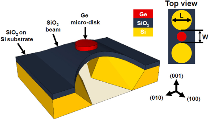
Figure 1. Three-dimensional sketch showing a Ge micro-disk on a suspended SiO2 beam with curved edges and supported by SiO2 on Si substrate. Fabrication design parameters, beam width (w), and beam length (l) are shown from a top-view in the top right corner. Axes orientation apply for the 3D sketch only.
GOI wafers were cleaned by diluted hydrofluoric (HF) and hydrochloric (HCl) acids. Then, Ge micro-disks were patterned using electron beam lithography with diameters ranging from 1 to 10 μm, and dry-etched using reactive-ion etching (RIE). To define the SiO2 beams such that they hold the Ge micro-disks on top, circular holes were dry-etched into the BOX layer on both sides of the micro-disk, as shown on the top right corner of Figure 1. Circular-hole openings allow manipulation of suspended beam dimensions, and thus tuning the strain, such that the diameter of the holes defines the beam length (l) and the minimum separation between them defines the beam width (w). Beam design parameters, l and w, were set to 36 and 12 μm, respectively. Before dry etching, the surface was passivated by 100 nm SiO2 deposited by plasma-enhanced chemical-vapor deposition (PECVD) at 350°C. To suspend the beams, we used 22% tetramethylammonium hydroxide (TMAH) solution to etch 10 μm of the supporting Si substrate.
For the SiO2 beams to be suspended, they have to be aligned with ⟨010⟩ directions (Süess et al., 2013) of the Si substrate, as shown in the optical microscopy image in Figure 2. Remarkably, anisotropy of TMAH etching through circular-hole openings on Si is pronounced along two directions: ⟨110⟩ at 45° relative to the beam direction ⟨010⟩, and ⟨210⟩ directions at 63.4° relative to the beam direction ⟨010⟩, as shown in Figure 2. After TMAH etching, beams were suspended and deflected either upwards or downwards. Direction of bending was not perfectly controlled; however, the majority of the devices were bent upward. We expect that upward bending will impose tensile strain on the top Ge micro-disks due to the longer length of the beam (Senturia, 2001).
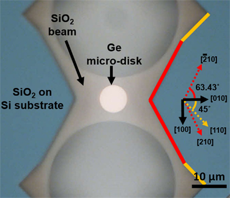
Figure 2. Optical microscopy image showing a Ge micro-disk on a suspended SiO2 beam, along with the crystal orientations of the Si substrate. Anisotropy of TMAH wet-etching of Si through circular hole openings is determined by ⟨110⟩ and ⟨210⟩ Si lattice orientations.
Laser interference microscopy imaging was used to create precise three-dimensional height maps of the devices in order to examine the bending behavior of the beams and Ge disks, which is related to the tensile strain. As shown by the laser interference microscopy image (Figure 3), the SiO2 beam is bent upward with a maximum deflection of approximately 0.8 μm. Height variations across the area of the Ge micro-disk was approximately 0.2 μm as seen in Figure 3. The bending of the disk edges may contribute to strain inhomogeneity across its height (Ghrib et al., 2013, 2014, 2015).
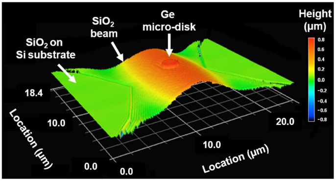
Figure 3. Laser interference microscopy image showing a three-dimensional height map of a Ge micro-disk on a suspended SiO2 beam.
Results and Discussion
Strain Characterization Using Raman Spectroscopy
In this section, we discuss the impact of beam suspension on Ge micro-disks by Raman spectroscopy. Tensile strain causes shrinkage of Ge band-gap (Peng et al., 2009; Süess et al., 2013; Sukhdeo et al., 2014), with a deformation rate that depends on its orientation, being either uni-axial or bi-axial (de Walle, 1989; Kurdi et al., 2010b). This tensile strain can be determined by Raman spectroscopy measurements, as tensile strain has the effect of red-shifting the Raman peak of bulk Ge (301 cm−1) according to the relation Δω = Sε, where Δω is the shift in wavenumbers, ε is the strain, and S is a proportionality coefficient. For bi-axial strain, S was reported as 390 cm−1 (Capellini et al., 2013, 2014). For ⟨001⟩ uni-axial strain, S was reported as 152 cm−1 (Peng et al., 2009; Süess et al., 2013; Sukhdeo et al., 2014).
We measured the strain using a laser with 532 nm wavelength and 2 μm spot size. Signals were collected through 3000 lines/mm grating with an exposure time of 10 s and 50 repetitions to enhance signal-to-noise ratio. The experimental data points were fitted by a Lorentzian to estimate peak positions. First, we examined excitation power dependence to identify the impacts of heating on the additional red-shift in the Raman peak position for suspended structures. The Raman shift was found to be linear against the excitation power; the rate was –6.3 × 10⁻⁴ cm−1/μW for a suspended 3-μm-diameter Ge disk, while the rate was –0.18 × 10⁻⁴ cm−1/μW for the un-patterned GOI wafer without suspension. In order to subtract the impact of heating, we linearly extrapolated the power dependence curves to find the interception of the Raman peak position.
The GOI wafer before patterning was slightly tensile-strained with a Raman shift of approximately –0.8 cm−1. This shift can be attributed to bi-axial tensile strain due to Ge on Si growth process, and the tensile strain value can then be calculated as εbiaxial ≈ 0.2%. Figure 4 shows the relative Raman shifts for Ge micro-disks with different diameters after suspension. We expected to apply uni-axial strain to the Ge disk by making a narrow bended beam; however, it is not straightforward to identify whether uni-axial strain overcame the original bi-axial strain. Assuming a bi-axial tensile strain is still dominant on the disks, a bi-axial tensile strain of 0.29, 0.28, and 0.35% is estimated for disks with a diameter of 1, 3, and 10 μm, respectively. On the other hand, if the uni-axial strain is dominant, the proportionality factor S is smaller, so that the corresponding strain values are estimated to be larger, 0.78, 0.73, and 0.92%, respectively. In reality, both uni-axial and bi-axial components should exist, and the actual strain values should be somewhere in between the above estimations.
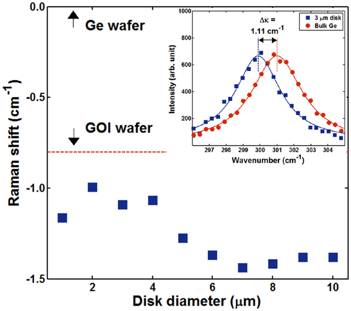
Figure 4. Raman shift (from bulk Ge) in cm−1 for suspended Ge micro-disks with different diameters. Top inset shows the actual Raman spectra for bulk Ge and 3 μm disk.
Uniformity of tensile strain is also critical for Ge direct-gap emission, since non-uniformity in strain would induce local variations of band-gap energies (de Walle, 1989; Kurdi et al., 2010b). Accordingly, electrons have a higher probability of dwelling regions with higher tensile strain, while converting less-strained regions into lossy mediums. As a result, the total overlap between gain regions and resonant modes may be reduced (Ghrib et al., 2013, 2014, 2015). In order to examine uniformity of strain distribution in our device, we scanned a two-dimensional Raman spectra of a 3 μm suspended Ge disk, with a step of 200 nm. The intensity distribution of Raman peaks of the Ge disk is shown in Figure 5A, while Figure 5B shows the actual Raman-shift distribution across the top surface of the disk. The black solid and dashed contour lines specify the regions with highest Raman intensity of more than 400 counts and 350 counts, respectively. It can be concluded from this mapping that a Raman shift of –1.11 cm−1 (0.28% bi-axial or 0.73% uniaxial tensile strain) exists over the majority of the Ge disk area. The stress seems to be relaxed at the circumference, which may be related to deformation of the disk at the edges.
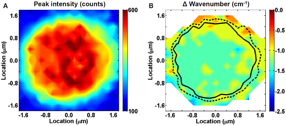
Figure 5. Two-dimensional Raman spectroscopy map of a suspended 3 μm Ge disk showing: (A) Raman intensity distribution and (B) actual Raman shift across the Ge surface. The black solid and dashed contour lines specify the regions with highest Raman intensity of more than 400 and 350 counts, respectively.
Photoluminescence and Direct-Gap Resonances
We performed finite-domain time-difference (FDTD) simulations using Lumerical FDTD software to estimate direct-gap resonances that exist in a 3 μm disk suspended on SiO2 beam, as shown in the inset of Figure 6. We chose the diameter to be 3 μm because WGM resonances were observed only in 3 μm disks as will be shown below. Thicknesses of Ge and SiO2 films are 100 and 145 nm, and refractive indexes were set to 4.2 and 1.45, respectively. We used an in-plane electric field source (εx,y →) assuming that only transverse-electric (TE) modes can be guided in 100 nm Ge (McCall et al., 1992; Boztug et al., 2013). The source pulse was chosen to have a Gaussian distribution centered around 1.7 μm to excite the modes within the direct-gap of Ge under slight tensile strain conditions. Simulation time was long enough to ensure clear visualization of resonant modes. The spectrum of the suspended 3 μm disk is shown in Figure 6, with resonant peaks identified as WGMs at 1.508, 1.561, 1.626, 1.708, and 1.811 μm. Surface plots of magnetic field component perpendicular to the plane of the disk of these resonances are shown on top of Figure 6. From these surface plots, we can label the TEm,n WGMs as TE13,1, TE12,1, TE11,1, TE10,1, and TE9,1, respectively, where m is the azimuthal number (number of full wavelengths across the inner circumference of the disk) and n is the radial number (number of field maxima along the radius).
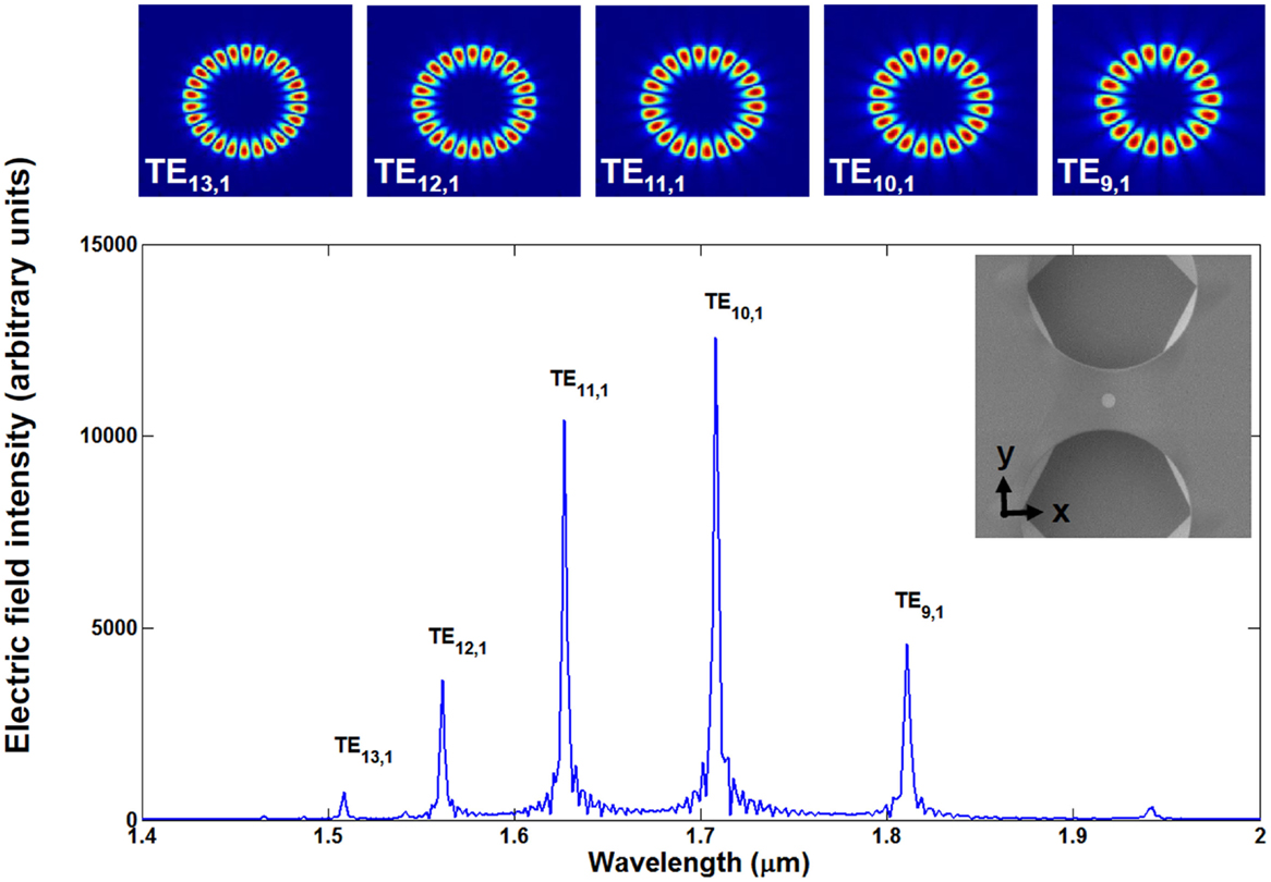
Figure 6. Spectrum of electric field (εx,y →) resonances in-plane of a 3 μm disk on a suspended SiO2 beam (shown in the SEM image inset). Confined modes with sharp peaks are whispering gallery modes as confirmed by the surface plots (top) of the vertical magnetic field component .
Photo-luminescence (PL) measurements were conducted at room temperature using a continuous-wave laser with a wavelength of 730 nm and approximately 2 μm spot size. Suspended Ge disks with diameters ranging from 1 to 10 μm were excited from top with 400 μW laser power. PL spectra for different disk sizes are shown in Figure 7A, which corresponds to Ge direct-gap recombinations (Sun et al., 2009; Kurdi et al., 2010a; Saito et al., 2011, 2014; Liu et al., 2012b). Accumulation of slight tensile strain within the Ge disks, as proved by Raman measurements, causes a corresponding red-shift in PL spectra (de Walle, 1989; Süess et al., 2013; Sukhdeo et al., 2014). The measured tensile strain values contribute to a red-shift of the direct-gap up to 1630–1640 nm (de Walle, 1989; Kurdi et al., 2010b), while the additional red-shift of the PL spectra is due to heating. Sharp-peak resonances were obtained for 3 μm disks only, and these peaks are attributed to WGMs occurring at 1591.5, 1704.4, and 1809.9 nm as shown in Figure 7B. Corresponding quality factors of 67, 182, and 191.8, respectively, were determined by fitting the resonant peaks with a Lorentzian. According to FDTD simulations, we identified these peaks to be TE11,1, TE10,1, and TE9,1 WGMs, respectively. On contrary, smaller disks with 1 and 2 μm diameters, suffered from extreme broadening in emission spectrum and no modulation by cavity resonances, were observed. This broadening can be explained by severe heating effects, due to the small disk diameters which were comparable to the spot size of the excitation laser. On the other hand, larger disks of 6, 8, and 10 μm diameter had broad-peak resonances. As the disk size increases, number of broad-peak resonances increases and free spectral range (FSR) between them decreases. The exact identification of these peaks is not straightforward; however, these resonances have broader peaks compared to WGMs observed in 3 μm disks, and consequently less important for monolithic operation. The reason for the absence of WGMs in larger disks would be related to the spot size of the laser (~2 μm), and only the center of the disks was excited.
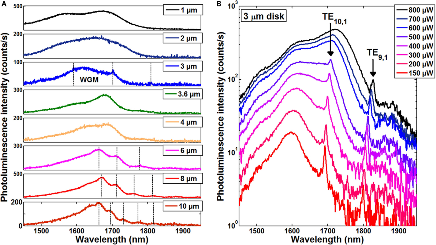
Figure 7. (A) Photoluminescence spectra of Ge micro-disks on suspended SiO2 beams with different diameters ranging from 1 μm to 10 μm using 400 μW excitation power, WGM are observed in the 3 μm disk spectrum, while broad-peak resonances are observed for 6, 8, and 10 μm disks. (B) Photoluminescence power-dependence of the suspended 3 μm Ge disk. The resonant WGMs are labeled as TE10,1 and TE9,1 according to FDTD simulations. At 800 μW pumping level, TE10,1 peak is invisible, while we can still observe TE9,1.
Figure 7B shows PL spectra of the suspended 3 μm disk for different excitation-power conditions. As the excitation power increases, the direct-gap emission intensity of the Ge disk increases. TE11,1 mode is barely visible on a log-scale figure because of its low intensity and Q-factor; presumably, it is highly affected by absorption from Ge due to its lower wavelength (Ishikawa et al., 2005; Wang et al., 2013). So, we will concentrate our discussions on TE10,1, and TE9,1. It was found that the intensities of TE10,1 and TE9,1 modes were proportional to P2.28 and P1.98, respectively, where P is the excitation power, as shown in Figure 8. This indicates that the tensile strain was not high enough to observe direct-gap characteristics. This agrees with our previous results (Al-Attili et al., 2015) in which we discussed the quadratic (∝P2) power dependence of emission intensities for intrinsic Ge, compared to a linear dependence (∝P1) for n-doped Ge. This difference was explained by the initial consumption of injected carriers in filling the L valleys in the case of intrinsic Ge due to its inherent in-direct band gap character, which causes a modest increase in emission intensity with power.
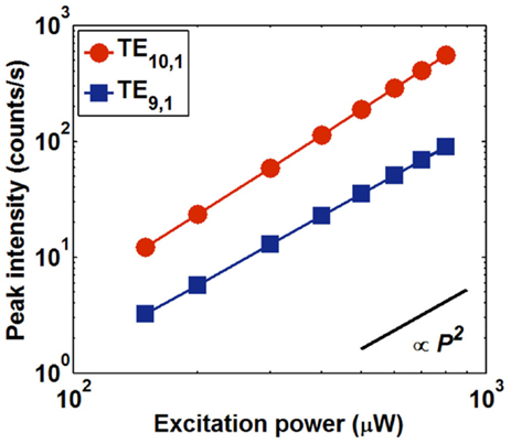
Figure 8. Excitation power dependence of the emission intensities for resonant whispering gallery modes at 1704.4 nm (TE10,1) and 1809.9 nm (TE9,1), observed in the 3 μm Ge disks.
Figure 9 shows the behavior of TE9,1 and TE10,1 Q-factors and resonant-peak positions as we increase the excitation power. A general trend of Q-factor degradation and red-shifting of resonant peaks with increased carriers’ injection is evident; this agrees with the work of other groups under optical (Shambat et al., 2010; Ghrib et al., 2013, 2014, 2015) and electrical (Cheng et al., 2011) pumping. Degradation of Q-factors with pumping has two main reasons: (I) heating which effectively shrinks Ge band-gap causing a red-shift in the direct-gap absorption edge (Ishikawa et al., 2003, 2005; Cannon et al., 2004; Liu et al., 2005; Wang et al., 2013), and consequently increasing the absorption coefficient at lower wavelengths. This loss mechanism affects high-energy (short wavelength) modes (Ishikawa et al., 2005; Lim et al., 2008; Wang et al., 2013). In addition to (II) the increase in free-carrier absorption (FCA) losses due to additional photo-induced carriers (Liu et al., 2007, 2012b; Kurdi et al., 2010b; Shambat et al., 2010), this loss mechanism is pronounced for lower energy (higher wavelength) resonances which suffer higher FCA (Liu et al., 2007; Kurdi et al., 2010b; Ghrib et al., 2013). Due to the association of both factors with injected carriers’ density, Q-factors of WGMs in Ge micro-disks are consequently affected by pumping levels. These excitation-related loss mechanisms cause broadening of resonant peaks until they become undetectable at high pumping powers, as shown in Figure 7B.
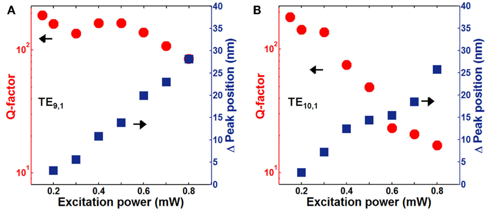
Figure 9. The effect of excitation power on Q-factor and peak position of (A) TE9,1 and (B) TE10,1. Increasing the power contributes to degradation in Q-factor and a red-shift in peak position. TE10,1 suffers higher degradation rate with excitation power, presumably due to the red-shift of direct-gap absorption edge of Ge with increasing excitation power due to heating, in addition to FCA losses. While TE9,1 being less affected by the Ge direct-gap absorption, undergoes increasing FCA losses with higher pumping levels.
Moreover, examining the different behavior of Q-factor degradation for different resonances according to Figure 9. It is obvious that up to 300 μW, the resonant peaks at 1704.4 nm (TE10,1) and 1809.9 nm (TE9,1) are broadened in a similar manner. However, as we keep increasing the excitation power above 300 μW, the lower-wavelength mode (TE10,1) undergoes a higher degradation rate, while the higher-wavelength mode (TE9,1) remains broadening at the same degradation rate. This can be explained as follows: at pump powers lower than 300 μW both modes are affected by FCA, while the red-shift in the Ge direct-gap absorption edge is not enough to approach TE10,1 yet. As we keep increasing the pump power, Ge direct-gap continues to red-shift due to heating until the direct-gap absorption totally overshadows the resonant peak of TE10,1 and we can no longer observe this peak at 600 μW, as shown in Figure 7. At this stage, the higher-wavelength mode is still suffering from increasing FCA but it remains unaffected by the Ge direct-gap absorption, and we still observe this peak even at 800 μW. This indicates that absorption due to heating is more significant than the FCA in preventing lasing. In order to avoid high injection levels and reduce absorption due to heating, higher tensile strain levels in addition to high n-type doping levels are required. n-type doping (Xu et al., 2014) also reduces FCA losses by allowing inversion with reduced levels of injected holes, which have a higher contribution to the total FCA compared to electrons (Liu et al., 2012b). There is a small dip in the Q-factor of TE9,1 around the pump power of 0.3 mW (Figure 9A), followed by a slight enhancement at 0.4 mW, before it starts to decrease again. This enhancement of Q-factor would be originating from the red-shift of the direct band edge toward the longer wavelengths due to heating, causing a partial offset in the FCA.
Conclusion and Future Work
In this paper, we have proposed a configuration to apply tensile strain on Ge micro-disks by suspension of the underlying SiO2 layer, for Ge monolithic emission purposes. We have shown that it is possible to accumulate tensile strain by using this structure. Further optimization has to be made in order to obtain higher tensile strain values. For instance, manipulating beams’ dimensions, BOX thickness, or depositing an additional stressor layer can be implemented to enhance tensile strain and reduce the lasing threshold. Uniformity of the applied strain was examined by performing a Raman scan and slight variations of strain at the disk edges were observed. PL spectra of suspended Ge disks with different diameters were discussed, and we identified sharp-peak WGMs only for the disk with the diameter of 3 μm, while broad-peak resonances existed in larger disks. We found that the achieved tensile stress was not enough to observe direct-gap characteristics, and heating effects were predominant for disk diameters smaller than 3 μm. Q-factors of WGMs were degraded with higher pump powers and this was related to the red-shift of the Ge direct-gap absorption edge and FCA. We also confirmed a quadratic power dependence of the emission intensity of intrinsic slightly strained Ge, which agrees with our previous results. We believe that Ge micro-disks hold great potential for future integration of low threshold CMOS-compatible laser sources and building a mature photonic circuitry on-chip.
Conflict of Interest Statement
The authors declare that the research was conducted in the absence of any commercial or financial relationships that could be construed as a potential conflict of interest.
Acknowledgments
We would like to thank research collaborators, engineers, and line managers in Hitachi, the University of Tokyo, and University of Southampton for supporting this project. Funding: Parts of the studies discussed here were supported by Japan Society for the Promotion of Science (JSPS) through its “Funding Program for World-Leading Innovation R&D on Science and Technology (FIRST Program),” the Project for Developing Innovation Systems, and Kakenhi 216860312, MEXT, Japan. This work is also supported by EPSRC Standard Grant (EP/M009416/1), EPSRC Manufacturing Fellowship (EP/M008975/1), EU FP7 Marie-Curie Carrier-Integration-Grant (PCIG13-GA-2013-618116), University of Southampton Zepler Institute Research Collaboration Stimulus Fund, and Hitachi.
References
Al-Attili, A. Z., Kako, S., Husain, M. K., Gardes, F. Y., Arimoto, H., Higashitarumizu, N., et al. (2015). Spin-on doping of germanium-on-insulator wafers for monolithic light sources on silicon. Jpn. J. Appl. Phys. 54, 052101. doi:10.7567/JJAP.54.052101
Bai, Y., Lee, K. E., Cheng, C., Lee, M. L., and Fitzgerald, E. A. (2008). Growth of highly tensile-strained Ge on relaxed InxGa1–x As by metal-organic chemical vapor deposition. J. Appl. Phys. 104, 084518. doi:10.1063/1.3005886
Boucaud, P., Kurdi, M. E., Ghrib, A., Prost, M., de Kersauson, M., Sauvage, S., et al. (2013). Recent advances in germanium emission. Photon. Res. 1, 102–109. doi:10.1364/PRJ.1.000102
Boztug, C., Sánchez-Pérez, J. R., Yin, J., Lagally, M. G., and Paiella, R. (2013). Grating-coupled mid-infrared light emission from tensilely strained germanium nanomembranes. Appl. Phys. Lett. 103, 201114. doi:10.1002/smll.201201090
Brinkman, W. F., Koch, T. L., Lang, D. V., and Wilt, D. P. (2000). The lasers behind the communications revolution. Bell Labs Tech. J. 5, 150–167. doi:10.1002/bltj.2212
Camacho-Aguilera, R. E., Cai, Y., Patel, N., Bessette, J. T., Romagnoli, M., Kimerling, L. C., et al. (2012). An electrically pumped germanium laser. Opt. Express 20, 11316–11320. doi:10.1364/OE.20.011316
Cannon, D. D., Liu, J., Ishikawa, Y., Wada, K., Danielson, D. T., Jongthammanurak, S., et al. (2004). Tensile strained epitaxial Ge film on Si(100) substrate with potential application to L-band telecommunications. Appl. Phys. Lett. 84, 906. doi:10.1063/1.1645677
Capellini, G., Kozlowski, G., Yamamoto, Y., Lisker, M., Wenger, C., Niu, G., et al. (2013). Strain analysis in SiN/Ge microstructures obtained via Si-complementary metal oxide semiconductor compatible approach. J. Appl. Phys. 113, 013513. doi:10.1063/1.4772781
Capellini, G., Reich, C., Guha, S., Yamamoto, Y., Lisker, M., Virgilio, M., et al. (2014). Tensile Ge microstructures for lasing fabricated by means of a silicon complementary metal-oxide-semiconductor process. Opt. Express 22, 399–410. doi:10.1364/OE.22.000399
Cheng, S. L., Shambat, G., Lu, J., Yu, H. Y., Saraswat, K., Kamins, T. I., et al. (2011). Cavity-enhanced direct band electroluminescence near 1550 nm from germanium microdisk resonator diode on silicon. Appl. Phys. Lett. 98, 211101. doi:10.1063/1.3592837
de Walle, C. G. V. (1989). Band lineups and deformation potentials in the model-solid theory. Phys. Rev. B 39, 1871. doi:10.1103/PhysRevB.39.1871
Fang, W., and Wickert, J. A. (1994). Post buckling of micromachined beams. J. Micromech. Microeng. 4, 116. doi:10.1088/0960-1317/4/3/004
Fischetti, M. V., and Laux, S. E. (1996). Band structure, deformation potentials, and carrier mobility in strained Si, Ge, and SiGe alloys. J. Appl. Phys. 80, 2234. doi:10.1063/1.363052
Ghrib, A., de Kersauson, M., Kurdi, M. E., Jakomin, R., Beaudoin, G., Sauvage, S., et al. (2012). Control of tensile strain in germanium waveguides through silicon nitride layers. Appl. Phys. Lett. 100, 201104. doi:10.1063/1.4718525
Ghrib, A., Kurdi, M. E., de Kersauson, M., Prost, M., Sauvage, S., Checoury, X., et al. (2013). Tensile-strained germanium microdisks. Appl. Phys. Lett. 102, 221112. doi:10.1364/OE.23.006722
Ghrib, A., Kurdi, M. E., Prost, M., de Kersauson, M., Largeau, L., Mauguin, O., et al. (2014). “Strain engineering in germanium microdisks,” in Proc. SPIE, 8990. San Francisco: SPIE. doi:10.1117/12.2037307
Ghrib, A., Kurdi, M. E., Prost, M., Sauvage, S., Checoury, X., Beaudoin, G., et al. (2015). All-around SiN stressor for high and homogeneous tensile strain in germanium microdisk cavities. Adv. Opt. Mater. 3, 353–358. doi:10.1002/adom.201400369
Goodman, J. W., Leonberger, F. J., Kung, S. Y., and Athale, R. A. (1984). Optical interconnections for VLSI systems. Proc. IEEE 72, 850–866. doi:10.1109/PROC.1984.12943
Ishikawa, Y., Wada, K., Cannon, D. D., Liu, J., Luan, H. C., and Kimerling, L. C. (2003). Strain-induced band gap shrinkage in Ge grown on Si substrate. Appl. Phys. Lett. 82, 2044. doi:10.1063/1.1564868
Ishikawa, Y., Wada, K., Liu, J., Cannon, D. D., Luan, H. C., Michel, J., et al. (2005). Strain-induced enhancement of near-infrared absorption in Ge epitaxial layers grown on Si substrate. J. Appl. Phys. 98, 013501. doi:10.1063/1.1943507
Jain, J. R., Hryciw, A., Baer, T. M., Miller, D. A. B., Brongersma, M. L., and Howe, R. T. (2012). A micromachining-based technology for enhancing germanium light-emission via tensile strain. Nat. Photonics 6, 398–405. doi:10.1038/nphoton.2012.111
Kurdi, M. E., Bertin, H., Martincic, E., de Kersauson, M., Fishman, G., Sauvage, S., et al. (2010a). Control of direct band gap emission of bulk germanium by mechanical tensile strain. Appl. Phys. Lett. 96, 041909. doi:10.1063/1.3297883
Kurdi, M. E., Fishman, G., Sauvage, S., and Boucaud, P. (2010b). Band structure and optical gain of tensile-strained germanium based on a 30 band k.p formalism. J. Appl. Phys. 107, 013710. doi:10.1063/1.3279307
Kurdi, M. E., David, S., Checoury, X., Fishman, G., Boucaud, P., Kermarrec, O., et al. (2008). Two-dimensional photonic crystals with pure germanium-on-insulator. Opt. Commun. 281, 846–850. doi:10.1016/j.optcom.2007.10.008
Liang, D., and Bowers, J. E. (2010). Recent progress in lasers on silicon. Nat. Photonics 4, 511–517. doi:10.1038/nphoton.2010.167
Lim, P. H., Kobayashi, Y., Takita, S., Ishikawa, Y., and Wada, K. (2008). Enhanced photoluminescence from germanium-based ring resonators. Appl. Phys. Lett. 93, 041103. doi:10.1063/1.2950087
Liu, J. (2014). Monolithically integrated Ge-on-Si active photonics. Photonics 1, 162–197. doi:10.3390/photonics1030162
Liu, J., Camacho-Aguilera, R., Bessette, J. T., Sun, X., Wang, X., Cai, Y., et al. (2012a). Ge-on-Si optoelectronics. Thin Solid Films 520, 3354–3360. doi:10.1016/j.tsf.2011.10.121
Liu, J., Kimerling, L. C., and Michel, J. (2012b). Monolithic Ge-on-Si lasers for large-scale electronic-photonic integration. Semicond. Sci. Technol. 27, 094006. doi:10.1364/OL.35.000679
Liu, J., Cannon, D. D., Wada, K., Ishikawa, Y., Jongthammanurak, S., Danielson, D. T., et al. (2005). Tensile strained Ge p-i-n photodetectors on Si platform for C and L band telecommunications. Appl. Phys. Lett. 87, 011110. doi:10.1063/1.1993749
Liu, J., Sun, X., Camacho-Aguilera, R., Kimerling, L. C., and Michel, J. (2010). Ge-on-Si laser operating at room temperature. Opt. Lett. 35, 679–681. doi:10.1364/OL.35.000679
Liu, J., Sun, X., Kimerling, L. C., and Michel, J. (2009). Direct-gap optical gain of Ge on Si at room temperature. Opt. Lett. 34, 1738–1740. doi:10.1364/OL.34.001738
Liu, J., Sun, X., Pan, D., Wang, X., Kimerling, L. C., Koch, T. L., et al. (2007). Tensile-strained, n-type Ge as a gain medium for monolithic laser integration on Si. Opt. Express 15, 11272–11277. doi:10.1364/OE.15.011272
McCall, S. L., Levi, A. F. J., Slusher, R. E., Pearton, S. J., and Logan, R. A. (1992). Whispering gallery mode microdisk lasers. Appl. Phys. Lett. 60, 289–291. doi:10.1063/1.106688
Menéndez, J., and Kouvetakis, J. (2004). Type-I Ge/Ge1–x–ySixSny strained-layer heterostructure with a direct Ge bandgap. Appl. Phys. Lett. 85, 1175. doi:10.1063/1.1784032
Michel, J., Liu, J., and Kimerling, L. C. (2010). High-performance Ge-on-Si photodetectors. Nat. Photonics 4, 527–534. doi:10.1038/nphoton.2010.157
Miller, D. A. B. (2009). Device requirements for optical interconnections to silicon chips. Proc. IEEE 97, 1166–1185. doi:10.1109/JPROC.2009.2014298
Nam, D., Kang, J. H., Brongersma, M. L., and Saraswat, K. C. (2014). Observation of improved minority carrier lifetimes in high-quality Ge-on-insulator using time-resolved photoluminescence. Opt. Lett. 39, 6205–6208. doi:10.1364/OL.39.006205
Nam, D., Sukhdeo, D. S., Kang, J. H., Petykiewicz, J., Lee, J. H., Jung, W. S., et al. (2013). Strain-induced pseudoheterostructure nanowires confining carriers at room temperature with nanoscale-tunable band profiles. Nano Lett. 13, 3118–3123. doi:10.1021/nl401042n
Ngo, T. P., Kurdi, M. E., Checoury, X., Boucaud, P., Damlencourt, J. F., Kermarrec, O., et al. (2008). Two-dimensional photonic crystals with germanium on insulator obtained by a condensation method. Appl. Phys. Lett. 93, 241112. doi:10.1063/1.3054332
Ortolland, C., Okuno, Y., Verheyen, P., Kerner, C., Stapelmann, C., Aoulaiche, M., et al. (2009). Stress memorization technique – fundamental understanding and low-cost integration for advanced CMOS technology using a nonselective process. IEEE Trans Electron Devices 56, 1690–1697. doi:10.1109/TED.2009.2024021
Peng, C. Y., Huang, C. F., Fu, Y. C., Yang, Y. H., Lai, C. Y., Chang, S. T., et al. (2009). Comprehensive study of the raman shifts of strained silicon and germanium. J. Appl. Phys. 105, 083537. doi:10.1063/1.3110184
Saito, S., Gardes, F. Y., Al-Attili, A. Z., Tani, K., Oda, K., Suwa, Y., et al. (2014). Group IV light sources to enable the convergence of photonics and electronics. Front. Mater. 1:1–15. doi:10.3389/fmats.2014.00015
Saito, S., Oda, K., Takahama, T., Tani, K., and Mine, T. (2011). Germanium fin light-emitting diode. Appl. Phys. Lett. 99, 241105. doi:10.1364/OE.22.005927
Shambat, G., Cheng, S. L., Lu, J., Nishi, Y., and Vuckovic, J. (2010). Direct band Ge photoluminescence near 1.6 μm coupled to Ge-on-Si microdisk resonators. Appl. Phys. Lett. 97, 241102. doi:10.1063/1.3526732
Süess, M. J., Geiger, R., Minamisawa, R. A., Schiefler, G., Frigerio, J., Chrastina, D., et al. (2013). Analysis of enhanced light emission from highly strained germanium microbridges. Nat. Photonics 7, 466–472. doi:10.1038/nphoton.2013.67
Sukhdeo, D. S., Nam, D., Kang, J. H., Brongersma, M. L., and Saraswat, K. C. (2014). Direct bandgap germanium-on-silicon inferred from 5.7% ⟨100⟩ uniaxial tensile strain. Photon. Res. 2, A8–A13. doi:10.1364/PRJ.2.0000A8
Sun, X., Liu, J., Kimerling, L. C., and Michel, J. (2009). Direct gap photoluminescence of n-type tensile-strained Ge-on-Si. Appl. Phys. Lett. 95, 011911. doi:10.1364/OL.38.000652
Suwa, Y., and Saito, S. (2011). “First-principles study of light emission from silicon and germanium due to direct tranistions,” in IEEE 8th Int. Conf. Group IV Photonics (London: IEEE), 222–224.
Virgilio, M., Manganelli, C. L., Grosso, G., Pizzi, G., and Capellini, G. (2013a). Radiative recombination and optical gain spectra in biaxially strained n-type germanium. Phys. Rev. B 87, 235313. doi:10.1103/PhysRevB.87.235313
Virgilio, M., Manganelli, C. L., Grosso, G., Schroeder, T., and Capellini, G. (2013b). Photoluminescence, recombination rate, and gain spectra in optically excited n-type and tensile strained germanium layers. J. Appl. Phys. 114, 243102. doi:10.1063/1.4849855
Wada, K., Liu, J., Jongthammanurak, S., Cannon, D. D., Danielson, D. T., Ahn, D., et al. (2006). Si Microphotonics for Optical Interconnection. Berlin: Springer Verlag.
Wang, X., Li, H., Camacho-Aguilera, R., Cai, Y., Kimerling, L. C., Michel, J., et al. (2013). Infrared absorption of n-type tensile-strained Ge-on-Si. Opt. Lett. 38, 652–654. doi:10.1364/OL.38.000652
Wilmsen, C. W., Thompson, E. G., and Meissner, G. H. (1972). Buckling of thermally-grown SiO2 thin-films. IEEE Trans. Electron Devices 19, 122. doi:10.1109/T-ED.1972.17381
Wirths, S., Geiger, R., von den Driesch, N., Mussler, G., Stoica, T., Mantl, S., et al. (2015). Lasing in direct-bandgap GeSn alloy grown on Si. Nat. Photonics 9, 88–92. doi:10.1038/nphoton.2014.321
Keywords: germanium, photonics, photoluminescence, strain, micro-cavity, whispering-gallery-mode
Citation: Al-Attili AZ, Kako S, Husain MK, Gardes FY, Higashitarumizu N, Iwamoto S, Arakawa Y, Ishikawa Y, Arimoto H, Oda K, Ido T and Saito S (2015) Whispering gallery mode resonances from Ge micro-disks on suspended beams. Front. Mater. 2:43. doi: 10.3389/fmats.2015.00043
Received: 26 March 2015; Accepted: 10 May 2015;
Published: 28 May 2015
Edited by:
Narayana Rao Desai, University of Hyderabad, IndiaReviewed by:
Raul J. Martin-Palma, Universidad Autónoma de Madrid, SpainJifeng Liu, Dartmouth College, USA
Copyright: © 2015 Al-Attili, Kako, Husain, Gardes, Higashitarumizu, Iwamoto, Arakawa, Ishikawa, Arimoto, Oda, Ido and Saito. This is an open-access article distributed under the terms of the Creative Commons Attribution License (CC BY). The use, distribution or reproduction in other forums is permitted, provided the original author(s) or licensor are credited and that the original publication in this journal is cited, in accordance with accepted academic practice. No use, distribution or reproduction is permitted which does not comply with these terms.
*Correspondence: Shinichi Saito, Faculty of Physical Sciences and Engineering, University of Southampton, B. 53/ R. 3013 Highfield Campus, University Road, Southampton, Hampshire, SO17 1BJ, UK,cy5zYWl0b0Bzb3Rvbi5hYy51aw==