 Md. Mehedi Hasan1
 Mst. Aysha Siddika2
 Md. Feroz Ali3*Md. Rafiqul Islam Sheikh1Abdullah Al Mamun4,5Md Jakir Hossen6*
- 1Department of Electrical and Electronic Engineering, Rajshahi University of Engineering and Technology, Rajshahi, Bangladesh
- 2Department of Electrical and Electronic Engineering, Pundra University of Science and Technology, Bogura, Bangladesh
- 3Department of Electrical and Electronic Engineering, Pabna University of Science and Technology, Pabna, Bangladesh
- 4Department of Electrical and Electrical Engineering, Feni University, Feni, Bangladesh
- 5School of Information and Communication Technology, Griffith University, Brisbane, QLD, Australia
- 6Center for Advanced Analytics (CAA), COE for Artificial Intelligence, Faculty of Engineering and Technology (FET), Multimedia University, Melaka, Malaysia
This study presents a next-generation lead-free perovskite solar cell (PVSC) architecture employing a dual-absorber design using MASnBr3 and ZnSnN2 to enhance photovoltaic performance while ensuring environmental sustainability. The proposed structure—FTO/n-ZnO/p-MASnBr3/p-+ZnSnN2/p-++CNTS/Au—was simulated and optimized using SCAPS-1D software. Extensive material and structural optimization was conducted, including selection of electron and hole transport layers as well as tuning absorber thickness, doping concentration, and defect density. The dual-absorber configuration leverages the complementary optical properties of MASnBr3 (bandgap: 1.3 eV) and ZnSnN2 (bandgap: 1.5 eV), enhancing spectral absorption and carrier separation. Optimization of interface properties, series/shunt resistance, and operating temperature further improved the device’s efficiency and stability. The final optimized structure achieved a power conversion efficiency (PCE) of 35.87%, with open-circuit voltage (VOC) of 1.17 V, short-circuit current density (JSC) of 34.39 mA/cm2, and fill factor (FF) of 89.01%. Quantum efficiency analysis confirmed near-unity photon-to-charge conversion across the visible spectrum. This work demonstrates the viability of combining lead-free perovskites with nitride absorbers for high-efficiency, eco-friendly solar technologies and provides a scalable pathway for future experimental validation and commercialization of sustainable photovoltaic systems.
1 Introduction
The development of renewable energy is a promising option due to the threat posed by climate change, the depletion of fossil fuels, the lack of energy storage, and massive energy production. Due to its sustainable and environmentally friendly low cost of generation, maintenance, and operation, solar energy has seen an unparalleled rise in the previous few decades and achieved crucial relevance in the field of renewable energy technology. Perovskite solar cells (PVSCs) are one of the newest third-generation photovoltaic (PV) technologies, and they have attracted a lot of interest because of their powerful exciton transitions, low processing temperature, tiny carrier effective masses, long carrier diffusion length, and high optical absorption (Zheng et al., 2018) (Malyukov et al., 2016). PVSCs, have a power conversion efficiency (PCE) of over 25% when used in a single junction configuration, have drawn a lot of interest in solar energy systems (Qin et al., 2023). Presently, the most efficient composition for PVSCs in the ABX3 perovskite structure is composed of a combination of lead (Pb) in the B positive ion area, methylammonium (CH3NH3+), caesium (Cs+), and formamidinium (NH2CHNH2+) in the A positive ion area, and either bromine (Br) or iodine (I) in the X positive ion area (Jiang et al., 2019). The first PVSCs using methylammonium lead iodide (CH3NH3PbI3) and methylammonium lead bromide (CH3NH3PbBr3) as solid sensitizers with liquid electrolytes in dye-sensitized solar cells (DSSCs) were reported in 2009 b y Kojima et al., a Tokyo-based group led by Tsutomu Miyasaka. (Kojima et al., 2009). Due to their dissolution in liquid electrolytes, MAPbBr3 and MAPbI3 DSSCs demonstrated low PCEs of 3.81% and 3.13% with a few-minute lifetimes, respectively (Arabpour Roghabadi et al., 2018). The PCE was reported to have increased to 10.9% in 2012 utilizing an organic halide meso superstructured perovskites solar cell, then to 20% in 2014. The PCE of the MAPbI3-based devices increased from 3.81 percent to 23.3 percent at a bandgap of 1.55 eV (Lee and Lee, 1979) (Yalçin and Öztürk, 2013) (Stoumpos et al., 2013) (Kojima et al., 2009) (Khatana and Mehra, 2019). However, because lead is poisonous and soluble in bodily fluids, it has an adverse effect on human health and, for the same reasons, poses a major obstacle to the widespread use of lead-based PVSCs (Needleman, 2004).
There are several lead-free perovskite absorber materials that have wide band gaps, making them viable substitutes for lead-containing perovskites. The discovery of non-lead PVSCs has prompted research into metal halides, including Sb, Ag, Sn, Cu, Ge, and Bi substitutes. In certain instances, Sn-based perovskite exhibits similar or better characteristics to Pb-based perovskite, such as scant exciton binding energy (<100 meV), narrow bandgap (1.28–1.55 eV), higher carrier mobility (102–103 cm2 V−1 s-1), long carrier diffusion length (102–105 nm) and long recombination time, high absorption coefficient (greater than 10–4 cm-1), and high conductivity (Hasan and Ahmed, 2021) (Eperon G. et al., 2014) (Watthage et al., 2018) (Li et al., 2019). Various perovskite absorber materials free of lead emissions Notable examples are caesium tin iodide (CsSnI3: 1.22 eV), formamidinium tin iodide (FASnI3: 1.41 eV), and methylammonium tin iodide (MASnI3: 1.3 eV) due to their wide band gaps, which make them viable substitutes for perovskites that contain toxic lead (Song et al., 2018). Because of their perfect band gap of 1.3 eV, perovskites with metal halides, as CH3NH3SnBr3 also have in particular emerged as viable possibilities for non-lead perovskite solar cells. The absorber layer of PVSCs was deposited using a variety of techniques, including spin coating, ink-jet printing, blade coating, thermal evaporation, and spray coating (Yadav and Kumar, 2024). Furthermore, lead-free MASnBr3 films were deposited using SnBr2 and MABr in the co-evaporation and sequential evaporation procedures (Jung et al., 2016). Solar cell efficiencies in co-evaporation-prepared perovskite films ranged from 0.03% to 0.35% when three distinct hole transport layers (HTLs) (spiro-OMeTAD, C60, and P3HT) were used. On the other hand, MASnBr3 perovskite films produced by sequential deposition were more efficient (1.12%) than those produced by co-evaporation. Furthermore, by altering absorber thickness, MASnBr3 was used as a light harvesting material to achieve different efficiency levels of 17.46, 21.66, and 23.66% (Mohammed et al., 2024) (Imani et al., 2023) (Kumavat and Sonvane, 2023). For Sn-based PVSCs, a potential PCE limit of approximately 30% has been calculated (Dixit et al., 2019). Thus, it can be concluded that the proposed perovskite structure (MASnBr3) is a great substitute for the most stable and efficient lead-free PVSC (Haneef et al., 2024a).
Due to the low efficiency of PVSCs in comparison to other solar cells, one layer of perovskite MASnBr3 and one layer of semiconductor zinc tin nitride (ZnSnN2) were utilized in this investigation as the active layer, which absorbs light. In contrast, the modelled structure uses ZnSnN2 as a second absorber since it is an attractive II-IV-V2 semiconductor material composed of inexpensive, nontoxic, and readily available materials (Aissat et al., 2016). The Zn-IV-N2 crystal structure is an orthorhombic wurtzite hexagonal shape. These III-N(III-V) pseudo-materials also have significant optical absorption coefficients, spontaneous polarization, and a direct bandgap, among other piezoelectric and optoelectronic characteristics (Laidouci et al., 2020). RF magnetron co-sputtering was used to deposit the ZnSnN2 films (Laidouci et al., 2020). The stoichiometry was ascertained by XRF (X-ray Fluorescence Spectroscopy), electrical measurements were made using the Hall effect, and the structure and phase purity of the films were assessed using XRD (X-Ray Diffraction) (Laidouci et al., 2020). In several earlier studies, ZnSnN2 was used as an absorber layer in solar cells with single and double absorber layer structures, which produced exceptional efficiency (Laidouci et al., 2023) (”31. Numerical simulation on an). Despite all these characteristics, ZnSnN2 is a suitable absorber layer since it boosts the overall stability of the suggested structure. Both MASnBr3 and ZnSnN2 are composed of earth-abundant, non-toxic elements like tin, zinc, nitrogen, and bromine, making them attractive for sustainable PV applications. Their precursors are relatively low-cost, and fabrication methods such as co-evaporation and RF sputtering are scalable, supporting the development of eco-friendly and commercially viable solar cells (Laidouci et al., 2020).
A numerical analysis of a unique lead-free PVSC architecture that incorporates two absorber layers is presented in this work. Two inherent photon absorber materials sandwiched between an n-doped ETL and a p-doped HTL make up a typical PVSC. Because of their effective charge carrier transportation management, the HTL and ETL are both crucial to the empowerment of PVSCs with high PCE. Here, we optimized the MASnBr3/ZnSnN2-based structure using six ETL (ZnO, TiO2, SnO2, SnS2, IGZO, and WS2) and eight types of HTL (CNTS (copper nickel tin sulfide), NiO, MoO3, Cu2O, CZTSe, CuI, P3H, and Spiro-OMeTAD). This revealed a new and stable structure that all reach the stable theoretical PCE. We have optimized the thickness and doping concentration of all HTLs and ETLs as well as the thickness of the absorbers layer, acceptor and donor doping charge concentration of the absorption layer, defect density of two absorber layers, interface defect density of the ETL/MASnBr3, and ZnSnN2/HTL layers, series and shunt resistance. In contrast, among all the optimized results, the combination of ZnO as ETL and CNTS as HLT in the FTO/n-ZnO/p-MASnBr3/p-+ZnSnN2/p-++CNTS/Back contact structure provides the maximum PCE of 35.87%.
2 Basic conceptual terms and device design
The SCAPS-1D software, which was created specially to investigate the optical and electrical properties that are advantageous for achieving a high degree of PCE, was used to carry out the simulation procedure. The Department of Electronics and Information Systems (ELIS) at the University of Ghent in Belgium is where the SCAPS software is developed (Kumar et al., 2024). In here, the band gap of the MASnBr3 material (1.3 eV) is somewhat over the ideal range for achieving high PCE in single junction PVSCs. To achieve high performance efficiency by expanding the light absorption regime from the low infrared region to the high infrared range of the electromagnetic spectrum, research has instead focused on adding an additional absorber layer (ZnSnN2) with a narrower bandgap below 1.5 eV. The addition of an absorber layer of lower bandgap material would enable the absorption regime to extend to the infrared region, whereas single junction-based PVSCs require an absorber layer within the (1.5 eV–1.3 eV) range. Figure 1A shows the several layers that make up the PVSC that we have built.
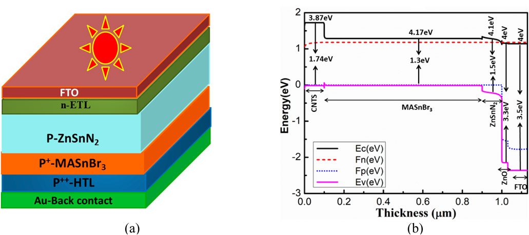
Figure 1. (a) Schematic layout of the PVSC with two absorbing layers and (b) energy band layout of FTO/n-ZnO/p-ZnSnN2/p+-MASnBr3/p++-CNTS/Au- back contact.
These layers consist of a platinum (Au) back metal electrode, an FTO layer, an ETL layer, a MASnBr3 absorber layer, another absorber layer of ZnSnN2, and an HTL layer. The addition of two energy-absorbing layers, MASnBr3 and ZnSnN2, improves the PVSCs’ efficiency. All forms of HTL (NiO, CNTS, MoO3, Cu2O, CZTSe, CuI, P3HT, and Spiro-OMeTAD) and ETL (TiO2, ZnO, SnO2, SnS2, IGZO, and WS2) were gradually evaluated in conjunction with a MASnBr3/ZnSnN2-based structure that revealed the HTL of CNTS and the ETL of ZnO combined structure offered the highest efficiency. The FTO/n-ZnO/p-ZnSnN2/p+-MASnBr3/p++-CNTS/Au-back contact structure’s arrangement is shown in Figure 1a. Figure 1b illustrates the energy band alignment of the optimized device architecture. Under equilibrium, the Fermi level aligns throughout the stack, ensuring built-in electric fields at the interfaces that drive charge separation. At the ETL/absorber interface, a small conduction band offset (CBO ≈ +0.1 eV) forms a modest spike that assists in selective electron extraction while minimizing backflow. Simultaneously, the absorber/HTL interface exhibits a slight valence band offset (VBO ≈ +0.05 eV), facilitating hole transport while suppressing recombination. Using SCAPS 1D-simulation software, the effects of each operational layer’s properties, such as the FTO/n-ZnO/p-ZnSnN2/p+-MASnBr3/p++-CNTS/Au-back contact device’s width, carrier, and density of defect, were evaluated. Using the Poisson and continuity equations for two charge carriers is the foundation of SCAPS-1D’s operation (Kumar et al., 2024). The technology allows for the construction of various types of solar cells by manipulating up to seven layers, and simulations may be carried out in both light and dark conditions. Poisson’s equation is used to generate the following Equation 1, which represents the p–n junction (Kumar et al., 2024):
In the context of solar cell film, the variable CA stands for the acceptor density and the variable CD for the donor density. Furthermore, h and e stand for holes and electrons, respectively, Ndef for trap concentration, ψ for electrostatic potential, and q for charge. The electron and hole continuity equations are the following Equations 2, 3 (Kumar et al., 2024) (Wahid et al., 2024):
In the provided equations, G represents the carrier generation rate, Re the electron recombination rate, and Rh the hole recombination rate. The symbols Je and Jp stand for electron and hole current density, respectively. The carrier current density can be computed using the electron and hole concentrations, which are represented by the following Equations 4, 5 (Bimli et al., 2023) (Nair et al., 2023):
here, the terms for electrons and holes, as well as the corresponding diffusion coefficients, are denoted by the letters De and Dh, respectively.
The Shockley Read Hall (SRH) recombination prototype is integrated into each design layer in this investigation. The following set of Equations 6–9 serves as the foundation for the SRH trap model (Nair et al., 2024):
where Vtℎ, Nt, σ, D, μ, K, T, and ζ stand for temperature-dependent motion of charge, mobility of charge, density of defect, capture area, coefficient of diffusion, Boltzmann constant, temperature, and carrier lifespan, respectively.
Tables 1, 3 display the PVSC architecture’s material specifications and provide a thorough rundown of the PVSC interface defect standard. To account for interface recombination effects, neutral interfacial defect parameters were incorporated at each layer junction, as summarized in Table 2. These include a defect density of 1 × 1010 cm-3 and symmetric electron/hole capture cross-sections (1 × 10⁻¹⁹ cm2), representing trap-assisted recombination at interfaces in a realistic manner (Kumar et al., 2024).
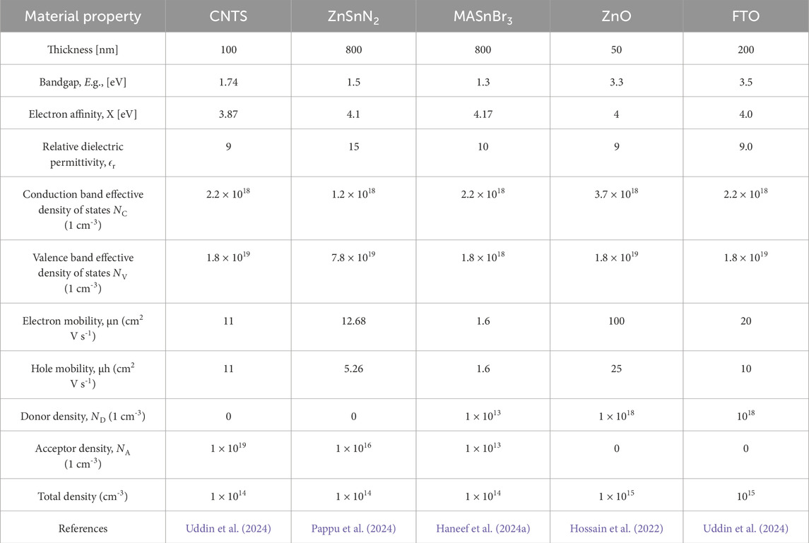
Table 1. Fundamental input parameters for our PVSC’s various materials.
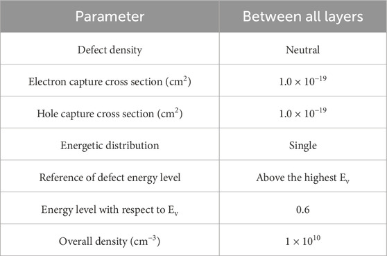
Table 2. Essential interfacial defect properties of the PVSC that was constructed (Kumar et al., 2024).
Additionally, all computer simulations are run with an incoming light brightness of 1000W/m2, which is equivalent to the mass of air (AM) 1.5G solar spectra, and the PVSC operates at a constant temperature of 300K. Furthermore, a perovskite solar cell’s series resistance should be as low as feasible to reduce resistive losses and guarantee that the load receives the maximum power produced by the cell (Sekar et al., 2020). Conversely, the shunt resistance value ought to be extremely high. By lowering leakage currents via other pathways, high shunt resistance preserves high VOC and FF (Sekar et al., 2020).
3 Results and discussion
3.1 Identifying the proper ETL
Identifying ETL is essential for optimizing charge extraction and improving overall performance in PVSCs. With Cu2O as HTL, six ETL materials ZnO, TiO2, SnO2, SnS2, IGZO, and WS2, were systematically evaluated. A series of simulations were performed to examine the impact of each ETL on the photovoltaic performance of the device. The energy band structure of ETLs is shown in Figure 2.
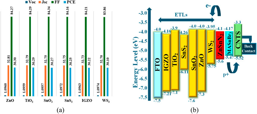
Figure 2. For different ETLs: (a) PV performance metrics, (b) energy band alignment for the MASnBr3/ZnSnN2 double-absorber structure.
The typical features of several ETLs are shown in Table 3, whereas Table 4 shows the PVSC performance metrics for various ETLs together with the associated CBOs.
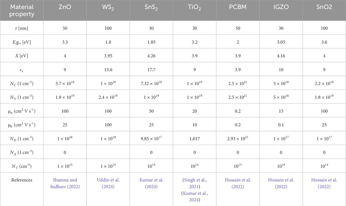
Table 3. Necessary input parameters for various ETLs.
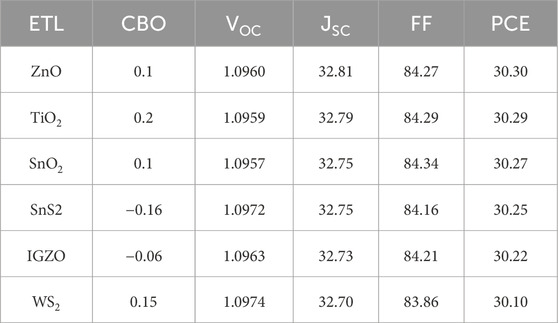
Table 4. Performance of the PVSC for different ETLs with CNTS as HTL.
To find the CBOs for the ETLs, the following Equation 10 is applied (Qaid et al., 2024):
Here,
3.2 Identifying the proper HTL
PVCs device efficiency is influenced by the HTL, which blocks electrons, lowers the electron-hole recombination rate, and facilitates hole migration from the MASnBr3/ZnSnN2 (absorber) layers to the back contact layer. A suitable bandgap, positive charge carrier mobility, ideal thickness, and an ideal doping charge concentration are all requirements for the HTL (Saikia et al., 2022). In this section, we use multiple hole transport layers (NiO, MoO3, Cu2O, CZTS, CuI, P3H, and Sprio-OMeTAD) to replicate the solar device efficiency in the original device configuration FTO/TiO2/MASnBr3/ZnSnN2/HTL/Au. The energy band structure of HTLs is shown in Figure 3. ZnO was initially kept as the ETL, but the HTLs were changed in order to evaluate the PVSC device’s electrical properties.
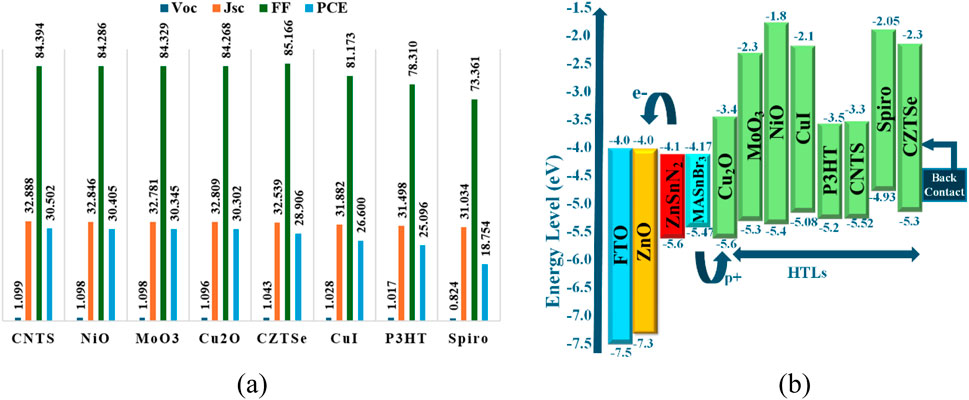
Figure 3. For different HTLs: (a) PV performance metrics, (b) energy band alignment for the MASnBr3/ZnSnN2 double-absorber structure.
The typical features of several HTLs are shown in Table 5, whereas Table 6 shows the PVSC performance parameters for various HTLs together with the associated VBO.
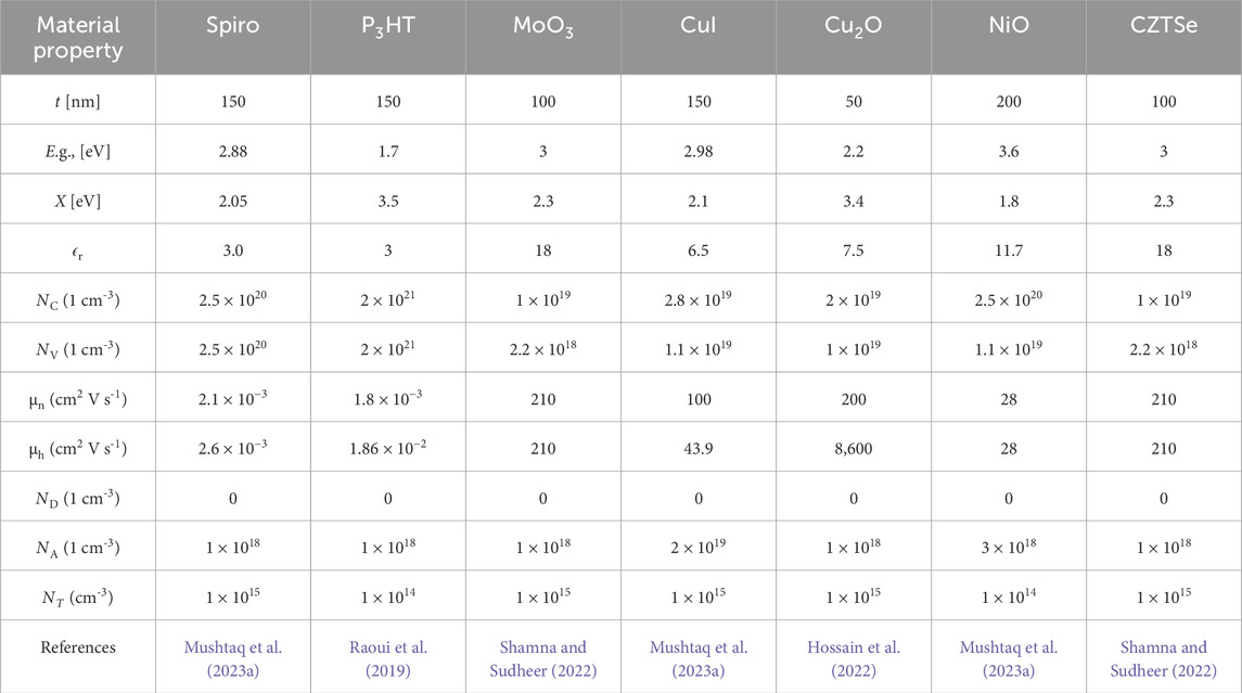
Table 5. Lists the necessary input parameters for various HTLs.
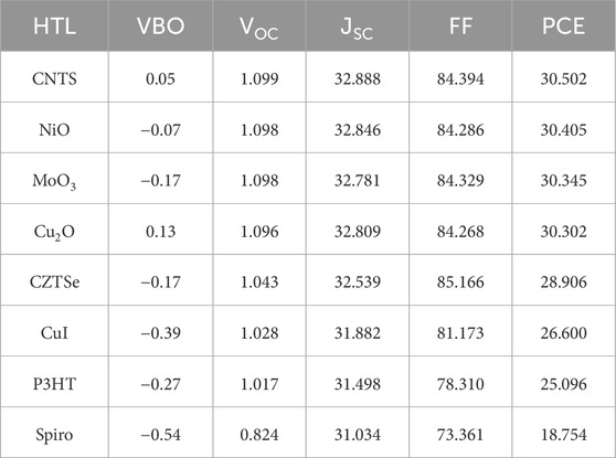
Table 6. Shows the PVSC’s performance for various HTLs using ZnO as the ETL.
The VBOs for different HTLs are calculated using the following Equation 11 (Qaid et al., 2024) as:
The symbols
Table 6 shows that CNTS is more effective than other HTLs. The CNTS HTL provides the highest PCE (30.50%) among the PVC layers, however the Spiro-OMeTED layer has the lowest PCE (18.75%). CNTS was chosen as the HTL based on its excellent energy level alignment with MASnBr3, exhibiting a VBO of +0.05 eV, which enables efficient hole extraction while minimizing recombination (Kumar et al., 2024). On the other hand, a tiny negative spike value increases the device’s PCE by lowering photon recombination at the junction interface. A significant negative VBO value may be an impediment to the passage of holes from the active layer to the HTL in the case of P3HT and Spiro-OMeTAD HTLs, which lowers the PCE of the PVSC. Out of all the HTL’s, the CNTS material had the highest values for JSC, VOC, and FF, measuring 32.88 mA/cm2, 1.09 V, and 84.39%, respectively. The CNTS is a promising option for the hole transport layer in perovskite solar cells because to its border bandgap energy of 1.74 eV (Khan et al., 2023). CNTSs have a variety of produced procedures, such as dip-coating from molecular ink, electrodeposition (Jariwala et al., 2018), (Patil et al., 2024), direct-coating from nanoparticle inks (Jariwala et al., 2017), (Rondiya et al., 2017), and the sol-gel approach (Ghosh et al., 2016). Together, CNTS’s favorable energy levels, earth-abundant composition, chemical stability, high hole mobility, easy synthesis, tunable properties, and reduced environmental impact (lead-free) suggest that it could help improve the sustainability and performance of PVSCs technologies (Uddin et al., 2024). Consequently, the CNTS material has been chosen as the HTL in our PVC design following an assessment of the electrical performance.
3.3 Determining the proper ETL thickness and donor doping concentration
Once the appropriate HTL for PVC was determined, we adjusted the ZnO ETL’s depth between 10 and 50 nm to examine its impact on PVC efficiency. Additionally, the donor concentration (ND) of the ETL is varied between 1014 cm−3 and 1020 cm−3, and the PVSC efficiency is calculated in order to examine the impact of the doping charge density on the PVSC efficiency. The performance of PVSC with respect to the thickness and ND of the ETL is depicted in Figure 4.
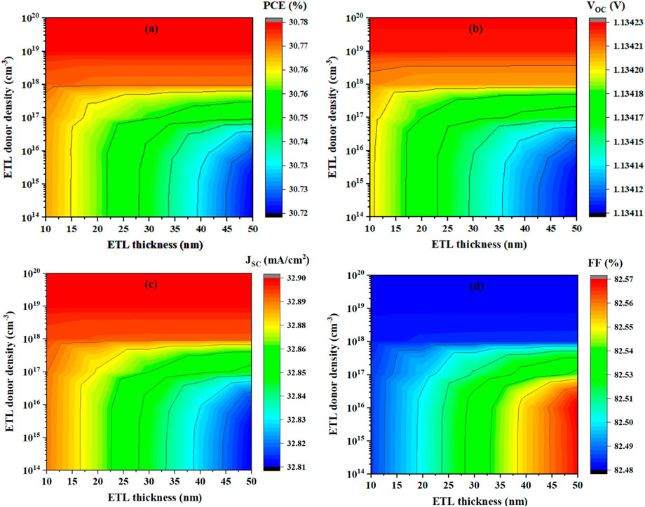
Figure 4. Effect of thickness and donor density on ETL performance: (a) PCE, (b) VOC, (c) JSC, and (d) FF.
The ETL’s thickness affects the charge transport’s velocity and efficiency. An optimal ETL thickness ensures efficient charge collection, increasing photo-generated current and overall device efficiency. A broad ETL acts as a barrier, preventing or lessening charge carrier recombination inside the active absorber material. Furthermore, the effectiveness of PVSC is significantly impacted by the electron carrier level in the ETL. On the other hand, a deeper ETL may absorb more incident photons, which could reduce the amount of light that reaches the photoactive perovskite layer. Conversely, a thin ETL might make it more likely that charge carriers will recombine inside the photoactive layer or at the ETL-perovskite interface. The efficient transfer of electrons to the electrode may be hampered by an inadequately thick ETL layer, which would lower device performance (Chabri et al., 2023). The device’s PCE first increases from roughly 30.72% to roughly 30.77% until the thickness reaches 30 nm, as seen in Figure 4. Additionally, thicker ETL causes FF and VOC to rise and then stabilize. But as thickness increases, JSC decreases. As a result, the ETL’s ideal thickness, taking into account all factors, is 30 nm.
On the other hand, as seen in Figure 6, the ND is increased to 1019 cm−3, and the PVSC device characteristics’ FF and PCE exhibit a notable increase followed by a decline. Conversely, JSC increases until ND reaches 1019 cm−3, beyond which it decreases. When the ND of ETL is raised to 1020 cm−3, the PVSC device properties show a significant decrease. Additionally, as the ND rises, VOC gradually decreases. The relationship between the increase in doping density and the concomitant rise in the ETL’s internal electric field is responsible for the growth in device PCE. This ultimately results in improved conductivity and charge transport motion (Qaid et al., 2024). However, too much doping results in the formation of Coulomb traps, which lowers electron mobility (Qaid et al., 2024). Therefore, for upcoming simulations, we will maintain the ETL’s ideal ND at 1019 cm−3.
3.4 Determining the proper HTL thickness and doping concentration
Since CNTS performs better than the other HTLs previously described, we have chosen it as an HTL. We are presently optimizing the CNTS layer thickness by altering it between 0.1 and 0.5 μm. Additionally, The HTL layers have a significant impact on the PVSC device’s efficacy in respect to acceptor concentration (NA). To investigate the effect of HTL, NA on PVSC device efficiency, we measured the PVSC device’s efficiency by altering the HTL layer’s NA between 1014 cm−3 and 1020 cm−3. Note that we do not alter any other materials, i.e., ZnO is utilized as the ETL and no interfacial layer is applied. Figure 5 shows how well the PVSC performs for varying NA and HTL (CNTS) thicknesses.
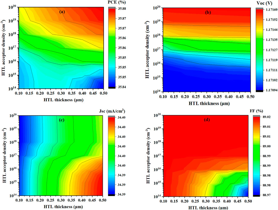
Figure 5. Effect of thickness and acceptor density on HTL performance: (a) PCE, (b) VOC, (c) JSC, and (d) FF.
It is evident from the graph that the variation in HTL thickness has minimal impact on our PVSC’s performance characteristics, specifically FF, JSC, VOC, and PCE. This is due to the fact that the depth of the HTL layer does not directly affect the VBO at the intersection of the perovskite layer film and the nearby HTL layer (Qaid et al., 2024). The energy levels of the materials in concern and the interface’s characteristics have the biggest effects on the VBO. However, longer lengths for holes to traverse from the perovskite layer to the interface may arise from a thicker HTL. Despite its potential advantages for charge transfer, excessive thickness might result in slower charge carriers, more resistive losses, and worse overall device efficiency. It may also increase the probability of charge carrier recombination. The quantity of photocurrent generated by the perovskite layer to the interface decreases as a result of holes’ increased propensity to recombine with electrons in the layer as they pass through a dense HTL. Despite its potential advantages for charge transfer, excessive thickness might result in slower charge carriers, more resistive losses, and worse overall device efficiency (Qaid et al., 2024). As a result, 0.5 μm has been chosen as the HTL’s thickness. On the other hand, As the NA is raised to 1020 cm−3, the PVSC device’s properties FF, JSC, VOC, and PCE show a discernible increase. The performance parameters of the PVSC gadget rapidly rise with increasing HTL doping concentration. The relationship between the rise in the electric field inside the HTL and the increase in doping charge concentration is responsible for the improvement in the device’s performance. As a result, conductivity and carrier transport velocity both rise (Haneef et al., 2024b). Therefore, we maintain the NA of the HTL at 1020 cm−3 for the simulations that follow.
3.5 Assessment of the suitable thickness of both active absorber layers
To optimize the thickness of the dual absorber layers MASnBr3 and ZnSnN2 a contour mapping approach was employed as illustrated in Figure 6. The performance parameters analyzed include PCE, VOC, JSC, and FF. Figure 6a shows that as the thicknesses of both MASnBr3 and ZnSnN2 increase, PCE also increases significantly, ranging from approximately 19% to over 31%. A similar trend is observed in JSC from Figure 6c, with values increasing up to 34.90 mA/cm2, indicating enhanced light absorption and carrier generation with thicker absorbers. On the other hand, Figure 6b illustrates that VOC reaches its peak of around 1.2 V at lower MASnBr3 thicknesses (<0.2 µm), but the variation across the range is minimal (1.10–1.21 V), and thus not critical in this optimization. Figure 6d reveals that FF is slightly higher at lower absorber thicknesses, varying from 80.48% to 84.42%. Despite the inverse behavior of FF with thickness, the overall efficiency gain justifies the selection of a thicker configuration. Therefore, the optimum thicknesses are chosen as MASnBr3 = 0.8 µm and ZnSnN2 = 0.1 µm. At this configuration, the corresponding performance metrics are VOC = 1.1135 V, JSC = 34.43 mA/cm2, FF = 81.79%, and PCE = 31.35%, demonstrating a balanced and efficient design for further device optimization.
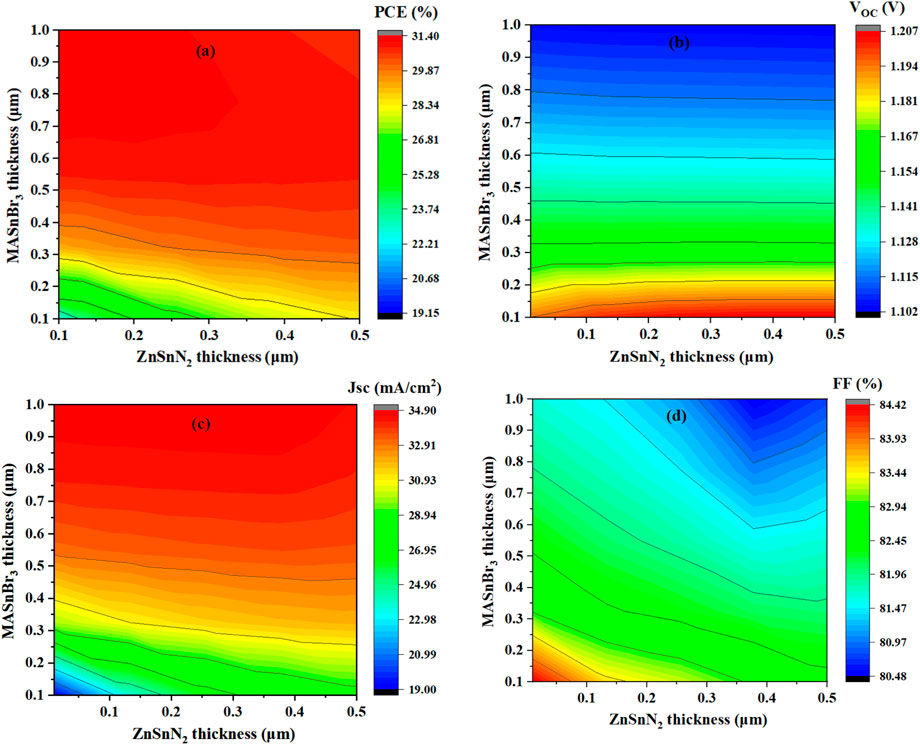
Figure 6. Effect of absorbers layer thickness on PVSC performance parameters: (a) PCE, (b) VOC, (c) JSC, and (d) FF.
3.6 Analysis of both active absorber layers’ appropriate carrier concentrations
The effect of acceptor density variation in both MASnBr3 and ZnSnN2 absorber layers on the performance of the solar cell was analyzed using contour plots, as shown in Figure 7. Figure 7a indicates that increasing the acceptor density of MASnBr3 significantly enhances PCE, while variation in ZnSnN2 acceptor density has a relatively minor effect. The highest efficiency is observed at lower ZnSnN2 acceptor density levels. This improvement in PCE with higher MASnBr3 doping can be attributed to the enhancement of built-in electric field strength, which improves charge carrier separation and reduces recombination losses. A similar trend is observed in the variation of VOC and FF, as shown in Figures 7b,d, where higher MASnBr3 acceptor density results in consistent performance gains. Figure 6c also confirms that high JSC values are obtained under these optimized conditions. Based on these findings, the optimal acceptor densities were selected as MASnBr3 = 1 × 1018 cm-3 and ZnSnN2 = 1 × 1013 cm-3. At this configuration, the device achieved a VOC of 1.1716 V, a JSC of 34.39 mA/cm2, an FF of 89.02%, and a PCE of 35.87%, confirming a substantial improvement in overall solar cell performance under these doping conditions.
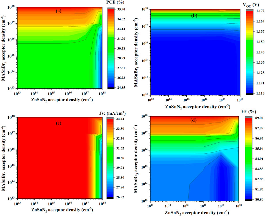
Figure 7. Effect of absorbers acceptor density on PVSC performance parameters (a) PCE, (b) VOC, (c) JSC, and (d) FF.
3.7 Examination of absorber defect density
The influence of total defect density in the absorber layers MASnBr3 and ZnSnN2 was examined by varying their respective values from 1 × 1013 cm-3 to 1 × 1018 cm-3, as presented in Figure 8. Figure 8a depicts the effect of MASnBr3 defect density on device performance. As the defect density increases, a pronounced decline in all key parameters PCE, VOC, JSC, and FF is observed. Specifically, PCE drops steeply from 35.88% at 1 × 1013 cm-3 to just 11.63% at 1 × 1018 cm-3. This degradation is primarily attributed to enhanced non-radiative recombination pathways that arise from the increased density of trap states, severely limiting charge carrier lifetimes (Eperon G. E. et al., 2014). In contrast, Figure 8b shows the effect of ZnSnN2 defect density. While all parameters exhibit a downward trend, the decline is less severe compared to MASnBr3. The PCE decreases from 35.94% at 1 × 1013 cm-3–25.30% at 1 × 1018 cm-3. Notably, JSC remains relatively stable across the range, indicating that light absorption and charge generation are less sensitive to defect density in the ZnSnN2 layer, although increased recombination still impacts VOC and FF. In our study, we have employed a defect density of 1 × 1013 cm-3 for MASnBr3 and 1 × 1014 cm-3 for ZnSnN2. At these conditions, the device maintains strong PV performance with a VOC of 1.1716 V, a JSC of 34.39 mA/cm2, an FF of 89.02%, and a PCE of 35.87%.
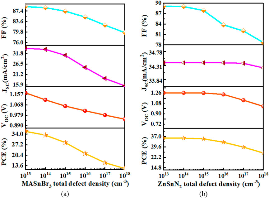
Figure 8. Analysis of absorbers defect density on PV performance parameters: (a) MASnBr3 (b) ZnSnN2.
3.8 Examination of the impact of resistance on PV measurements
The impact of series resistance RS and shunt resistance RSh on the PV performance of the dual-absorber solar cell was examined, as illustrated in Figure 9. The values of RS were varied from 0 to 6 Ω cm-2, while RSh was swept from 10 to 106 Ω cm-2. An increase in RS shows a clear detrimental effect on all performance metrics. PCE drops from 35.99% at RS = 0 Ω cm-2–29.30% at RS = 6 Ω cm-2. This decline is driven primarily by the drop in FF, while JSC and VOC remain largely unchanged. In contrast, increasing RSh significantly improves device performance. At low RSh = 10 Ω cm-2, the device shows poor metrics with PCE = 2.93%, VOC = 0.344 V, and FF = 25.00%. As RSh increases, leakage currents are suppressed, leading to a rapid enhancement in all parameters. At RSh ≥ 105 Ω cm-2, performance saturates. According to previous studies (Karthick et al., 2020), maintaining a low series resistance is crucial to minimize internal power losses and ensure efficient power transfer to the external load. Meanwhile, a high shunt resistance is necessary to suppress leakage currents and uphold high VOC and FF (Karthick et al., 2020). In alignment with these insights and supported by other simulation-based investigations (Sunny et al., 2021), we selected a realistic RS of 0.1 Ω cm-2 and RSh of 1 × 10⁶ Ω cm-2 in our simulations to emulate practical conditions and optimize device efficiency.
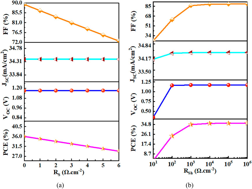
Figure 9. Analysis of resistance effect on PV metrics: (a) RS (b) RSh.
3.9 Influence of temperature on solar cell performance
The influence of temperature on the performance of the dual-absorber solar cell was examined over a range from 300 K to 440 K, as shown in Figure 10. Figure 10a presents the variation of key PV parameters PCE, VOC, JSC, and FF with temperature. As temperature increases, a notable decline in both VOC and FF is observed, leading to a corresponding reduction in PCE. Specifically, efficiency drops from 35.88% at 300 K to 30.57% at 440 K. The decline in VOC with increasing temperature is attributed to the enhanced intrinsic carrier concentration and increased recombination activity at higher temperatures, which reduces the quasi-Fermi level splitting. Similarly, FF degrades due to elevated series resistance and reduced built-in electric field strength. In contrast, JSC remains relatively stable throughout the temperature range, indicating that photogeneration is not significantly affected. Figure 10b further confirms this trend through the J–V characteristics at various temperatures, where the FF and VOC both diminish as temperature rises. This inverse relationship between temperature and solar cell performance is well-documented in literature, where it has been shown that elevated temperatures adversely affect charge carrier recombination and material interface stability (”31. Numerical simulation on an).
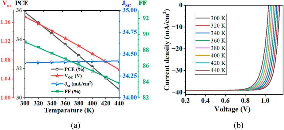
Figure 10. (a) Temperature effect on solar cell performance (b) JV curve at different temperatures.
3.10 Quantum efficiency and device optimization
Figure 11a shows the quantum efficiency (QE) graph of the solar cell. The device exhibits excellent spectral response, maintaining nearly 100% QE in the visible range, indicating efficient light harvesting and charge collection throughout the working wavelength range. The QE declines at higher wavelengths beyond 850 nm, consistent with the optical absorption limits of the absorber materials. Figure 11b presents the current voltage (J–V) characteristics before and after optimization. Initially, based on the calculated IV-curve, the solar cell exhibited the following performance: VOC = 1.0974 V, JSC = 32.70 mA/cm2, FF = 83.86%, and PCE = 30.10%. To improve performance, a step-by-step optimization procedure was employed. Initially, the ETL and HTL were selected based on favorable band alignment and their contribution to the overall device metrics. In this process, ZnO was selected as the ETL and CNTS as the HTL due to their suitable energy levels and compatibility. Following the material selection, the thicknesses of the ETL, HTL, and both absorber layers (ZnSnN2 and MASnBr3) were optimized. The optimum ETL thickness was determined to be 30 nm, and the donor density of ZnO was set to 1 × 1019 cm-3. The MASnBr3 absorber thickness was optimized to 0.8 µm and its acceptor density to 1 × 1018 cm-3. For the ZnSnN2 absorber, a thickness of 0.1 µm and acceptor density of 1 × 1013 cm-3 were found to be optimal. The HTL thickness was adjusted to 500 nm, with an optimized acceptor density of 1 × 1020 cm-3. After completing these optimizations, the solar cell demonstrated significant improvements across all performance indicators. The final device performance reached VOC = 1.1716 V, JSC = 34.40 mA/cm2, FF = 89.02%, and a PCE of 35.88%, confirming the effectiveness of the comprehensive optimization strategy and material selections in achieving a high-efficiency dual-absorber solar cell.
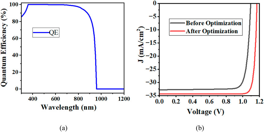
Figure 11. (a) Quantum Efficiency and (b) device optimization analysis of MASnBr3/ZnSnN2 based PVSCs.
3.11 The performance metrics of previously published publications on PVSCs are compared to our study
The search for high-efficiency and eco-friendly solar tech has led to extensive development of Pb-free perovskite and nitride-based absorbers. Table 7 presents a detailed comparison of the PV performance of our proposed n-ZnO/p-MASnBr3/p-+ZnSnN2/p-++CNTS heterostructure with previously reported devices. Arca et al. (Arca et al., 2017) explored ZnSnN2 based structures incorporating Mg:CuCrO2 as HTL and achieved a PCE of 23.5%, limited by moderate Jsc. With improvements in absorber quality and interface tuning, Laidouci et al. (Laidouci et al., 2020) reported 22.32% efficiency using CuCrO2 as HTL. In a subsequent study (Laidouci et al., 2023), integrating a Si BSF pushed the PCE to 29.5%.
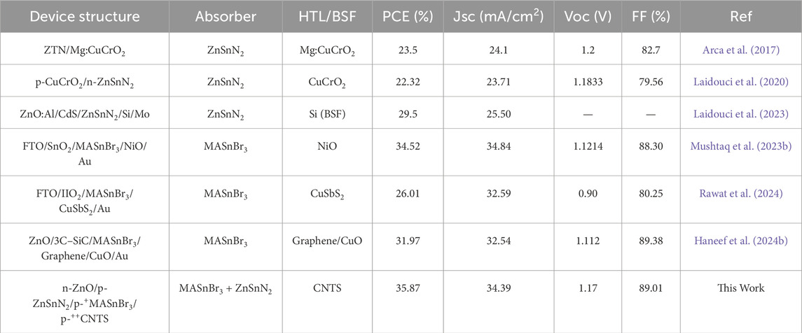
Table 7. Comparison with other work.
Meanwhile, MASnBr3 based devices have shown notable promise. Mushtaq et al. (Haneef et al., 2024a) demonstrated a planar FTO/SnO2/MASnBr3/NiO/Au stack with 34.52% PCE. Rawat et al. (Rawat et al., 2024) investigated temperature-dependent MASnBr3 performance and achieved 26.01% using CuSbS2 as HTL. Haneef et al. (Haneef et al., 2024b) introduced graphene and 3C–SiC interface layers, reaching 31.97%.
In comparison, the dual-absorber structure proposed here combining MASnBr3 and ZnSnN2 achieved a PCE of 35.87%, outperforming all previous reports. The graded absorber strategy leverages the complementary bandgap of MASnBr3 (1.3eV) and ZnSnN2 (1.5 eV), enhancing carrier collection and reducing losses. Optimized thickness, doping, and defect further improved performance. This highlights the importance of absorber engineering and interface tuning for next-gen, high efficiency, Pb-free PVSCs.
3.12 Experimental pathway and fabrication challenges
A future experimental validation of the proposed MASnBr3/ZnSnN2-based photovoltaic structure can follow scalable, low-cost fabrication approaches already explored for similar materials. MASnBr3 thin films can be synthesized using solution-based methods such as spin coating or ultrasonic spray pyrolysis (USP), or vacuum-based methods like sequential thermal evaporation or co-evaporation of SnBr2 and methylammonium bromide (MABr) precursors (Kaleli et al., 2022), (Wang et al., 2025). Among these, sequential evaporation has yielded better film quality and higher efficiencies (up to 1.12%) than co-evaporation due to better phase control and stoichiometry. Additionally, fully USP-fabricated structures have been demonstrated using FTO/TiO2/MASnBr3/P3HT/Ag configurations.
For ZnSnN2, RF magnetron co-sputtering is a well-established technique that provides high purity and stoichiometric control (Laidouci et al., 2020). This method allows co-deposition from Zn and Sn targets in a nitrogen plasma environment. Stoichiometry can be verified by XRF, while phase purity and crystallinity can be confirmed via XRD. Hall effect measurements can assess carrier mobility and type.
MASnBr3 faces major challenges with Sn2+ oxidation to Sn4+ in ambient conditions, leading to rapid degradation. This can be addressed through encapsulation techniques such as ALD-deposited Al2O3, parylene coatings, or by introducing reducing additives during synthesis to stabilize Sn2+ (Noel et al., 2014), (Li et al., 2016), (Raiford, 2021). On the other hand, ZnSnN2 requires precise stoichiometry control and annealing optimization to minimize defects and maintain phase purity (Bui, 2022). Its metastable wurtzite structure can be sensitive to temperature and growth conditions. Additionally, interface engineering is crucial. Proper alignment and passivation of the MASnBr3/ZnSnN2 interface can suppress recombination and enhance charge transfer. Experimental deposition order and interlayer treatment (e.g., surface treatments or insertion of ultra-thin buffer layers) may play a key role. Together, the integration of sequential evaporation for MASnBr3 and RF co-sputtering for ZnSnN2, followed by post-deposition annealing and encapsulation, represents a viable experimental roadmap to replicate the high-efficiency dual-absorber structure proposed in this simulation study.
4 Conclusion
In this study, we proposed and optimized a lead-free perovskite solar cell using a dual-absorber configuration of MASnBr3 and ZnSnN2. Through SCAPS-1D simulation, we demonstrated that careful selection and tuning of (ETL) ZnO and (HTL) CNTS, along with optimization of absorbers thickness, doping, and defect densities, can significantly enhance device performance. The optimized device achieved a high PCE of 35.87%, with VOC = 1.17 V, JSC = 34.39 mA/cm2, and FF = 89.01%. Encapsulation strategies were noted as essential for improving MASnBr3 stability under ambient conditions. Moreover, both absorber materials consist of earth-abundant and non-toxic elements, supporting sustainability and scalability.
Data availability statement
The raw data supporting the conclusions of this article will be made available by the authors, without undue reservation.
Author contributions
MH: Resources, Validation, Visualization, Project administration, Conceptualization, Formal Analysis, Data curation, Writing – review and editing, Methodology, Writing – original draft, Investigation, Software, Supervision. MSi: Supervision, Software, Methodology, Validation, Conceptualization, Data curation, Investigation, Writing – original draft, Formal Analysis, Writing – review and editing, Resources, Visualization, Project administration. MA: Writing – review and editing, Investigation, Software, Conceptualization, Funding acquisition, Resources, Project administration, Methodology, Validation, Supervision, Data curation, Formal Analysis, Visualization. MSh: Validation, Data curation, Supervision, Conceptualization, Writing – review and editing, Project administration, Software, Resources, Formal Analysis. AA: Funding acquisition, Validation, Resources, Project administration, Supervision, Investigation, Writing – review and editing, Methodology, Visualization, Software. MH: Resources, Funding acquisition, Project administration, Formal Analysis, Data curation, Validation, Writing – review and editing, Conceptualization, Supervision, Investigation, Methodology.
Funding
The author(s) declare that financial support was received for the research and/or publication of this article. This research did not receive any specific grant from funding agencies in the public, commercial, or not-for-profit sectors.
Acknowledgments
Dr. Marc Burgelman of the University of Gent in Belgium is to be thanked by the authors for supplying the SCAPS simulator. The authors also would like to express their sincere gratitude to Pabna University of Science and Technology, Pabna, Bangladesh, and Rajshahi University of Engineering and Technology, Rajshahi, Bangladesh, for providing renewable energy laboratory facilities and the necessary support to carry out this research.
Conflict of interest
The authors declare that the research was conducted in the absence of any commercial or financial relationships that could be construed as a potential conflict of interest.
Generative AI statement
The author(s) declare that no Generative AI was used in the creation of this manuscript.
Publisher’s note
All claims expressed in this article are solely those of the authors and do not necessarily represent those of their affiliated organizations, or those of the publisher, the editors and the reviewers. Any product that may be evaluated in this article, or claim that may be made by its manufacturer, is not guaranteed or endorsed by the publisher.
References
Aissat, A., Arbouz, H., Nacer, S., Benyettou, F., and Vilcot, J. P. (2016). Efficiency optimization of the structure pin-InGaN/GaN and quantum well-InGaN for solar cells. Int. J. Hydrogen Energy 41 (45), 20867–20873. doi:10.1016/j.ijhydene.2016.06.028
Arabpour Roghabadi, F., Ahmadi, N., Ahmadi, V., Di Carlo, A., Oniy Aghmiuni, K., Shokrolahzadeh Tehrani, A., et al. (2018). Bulk heterojunction polymer solar cell and perovskite solar cell: concepts, materials, current status, and opto-electronic properties. Sol. Energy 173, 407–424. doi:10.1016/j.solener.2018.07.058
Arca, E., Fioretti, A., Lany, S., Tamboli, A. C., Teeter, G., Melamed, C., et al. (2017). Band edge positions and their impact on the simulated device performance of ZnSnN2-based solar cells. EEE J. Photovolt., 8, 110–117. doi:10.1109/JPHOTOV.2017.2766522
Bimli, S., Manjunath, V., Mulani, S., Miglani, A., Game, O., and Devan, R. (2023). Theoretical investigations of all inorganic Cs2SnI6 double perovskite solar cells for efficiency ∼ 30 %. Sol. Energy 256, 76–87. doi:10.1016/j.solener.2023.03.059%,”
Bui, N. K. T., “Growth of earth abundant material based thin films by sputtering technique for photovoltaics,” 2022.
Chabri, I., Benhouria, Y., Oubelkacem, A., Kaiba, A., Essaoudi, I., and Ainane, A. (2023). SCAPS device simulation study of formamidinium Tin-Based perovskite solar Cells: investigating the influence of absorber parameters and transport layers on device performance. Sol. Energy 262, 111846. doi:10.1016/j.solener.2023.111846
Dixit, H., Punetha, D., and Pandey, S. K. (2019). Improvement in performance of lead free inverted perovskite solar cell by optimization of solar parameters. Opt. (Stuttg) 179, 969–976. doi:10.1016/j.ijleo.2018.11.028
Eperon, G., Stranks, S., Menelaou, C., Johnston, M., Herz, L., and Snaith, H. (2014a). Formamidinium lead trihalide: a broadly tunable perovskite for efficient planar heterojunction solar cells. Energy Environ. Sci. 7, 982–988. doi:10.1039/C3EE43822H
Eperon, G. E., Burlakov, V. M., Docampo, P., Goriely, A., and Snaith, H. J. (2014b). Morphological control for high performance, solution-processed planar heterojunction perovskite solar cells. Adv. Funct. Mater. 24 (1), 151–157. doi:10.1002/adfm.201302090
Ghosh, A., Biswas, A., Thangavel, R., and Udayabhanu, G. (2016). Photo-electrochemical properties and electronic band structure of kesterite copper chalcogenide Cu2–II–Sn–S4 (II = Fe, Co, Ni) thin films. RSC Adv. 6 (98), 96025–96034. doi:10.1039/C6RA15700A
Hossain, M. K., Arnab, A. A., Das, R. C., Hossain, K. M., Rubel, M. H. K., Rahman, M. F., et al. (2022). Combined DFT, SCAPS-1D, and wxAMPS frameworks for design optimization of efficient Cs 2 BiAgI 6-based perovskite solar cells with different charge transport layers. RSC Adv. 12 (54), 34850–34873. doi:10.1039/d2ra06734j
Haneef, M., Tahir, S., Mahmoud, H. A., Ali, A., and Ashfaq, A. (2024a). Optimizing lead-free MASnBr3 perovskite solar cells for high-efficiency and long-term stability using graphene and advanced interface layers. ACS Omega 9 (6), 7053–7060. doi:10.1021/acsomega.3c08981
Haneef, M., Tahir, S., Mahmoud, H., Ali, A., and Ashfaq, A. (2024b). Optimizing lead-free MASnBr 3 perovskite solar cells for high-efficiency and long-term stability using graphene and advanced interface layers. ACS Omega 9 (Jan), 7053–7060. doi:10.1021/acsomega.3c08981
Hasan, B., and Ahmed, N. (2021). Feature selection technique applied in Medical application by Supervised algorithm. A Rev. doi:10.5281/zenodo.4543647
Hossain, M. K., Arnab, A. A., Das, R. C., Rubel, M. H. K., Rahman, M. F., et al. (2022). Combined DFT, SCAPS-1D, and WxAMPS frameworks for design optimization of efficient Cs2BiAgI6-based perovskite solar cells with different charge transport layers. RSC Adv. 12 (54), 34850–34873. doi:10.1039/d2ra06734j
Imani, S., Seyed-Talebi, S. M., Beheshtian, J., and Diau, E. W. G. (2023). Simulation and characterization of CH3NH3SnI3-based perovskite solar cells with different Cu-based hole transporting layers. Appl. Phys. A 129 (2), 143. doi:10.1007/s00339-023-06428-0
Jariwala, A., Chaudhuri, T., Patel, S., Toshniwal, A., Kheraj, V., and Ray, A. (2017). Direct-coated copper nickel tin sulphide (Cu 2 NiSnS 4) thin films from molecular ink. Mater. Lett. 215, 118–120. doi:10.1016/j.matlet.2017.12.083
Jariwala, A., Chaudhuri, T. K., Patel, S., Toshniwal, A., Kheraj, V., and Ray, A. (2018). Direct-coated copper nickel tin sulphide (Cu2NiSnS4) thin films from molecular ink. Mater. Lett. 215, 118–120. doi:10.1016/j.matlet.2017.12.083
Jiang, Q., Zhao, Y., Zhang, X., Yang, X., Chen, Y., Chu, Z., et al. (2019). Surface passivation of perovskite film for efficient solar cells. Nat. Photonics 13 (1), 460–466. doi:10.1038/s41566-019-0398-2
Jung, M.-C., Raga, S. R., and Qi, Y. (2016). Properties and solar cell applications of Pb-free perovskite films formed by vapor deposition. RSC Adv. 6 (4), 2819–2825. doi:10.1039/C5RA21291J
Kaleli, M., Şen, E., Lapa, H. E., and Aldemir, D. A. (2022). The production route of the MASnBr3 based perovskite solar cells with fully ultrasonic spray pyrolysis method. Phys. B Condens. Matter 645, 414293. doi:10.1016/j.physb.2022.414293
Karthick, S., Velumani, S., and Bouclé, J. (2020). Experimental and SCAPS simulated formamidinium perovskite solar cells: a comparison of device performance. Sol. Energy 205, 349–357. doi:10.1016/j.solener.2020.05.041
Khan, Z., Noman, M., Tariq, S., and Daud, A. (2023). Systematic investigation of the impact of kesterite and zinc based charge transport layers on the device performance and optoelectronic properties of ecofriendly tin (Sn) based perovskite solar cells. Sol. Energy 257 (March), 58–87. doi:10.1016/j.solener.2023.04.019
Khatana, C., and Mehra, D. R. (2019). Device simulation of lead-free MASnI3 solar cell with CuSbS2 (copper antimony sulfide). J. Mater. Sci. 54, 5615–5624. doi:10.1007/s10853-018-03265-y
Kojima, A., Teshima, K., Shirai, Y., and Miyasaka, T. (2009). Organometal halide perovskites as visible-light sensitizers for photovoltaic cells. J. Am. Chem. Soc. 131 (17), 6050–6051. doi:10.1021/ja809598r
Kumar, N., Agarwal, A., Singh, A., and Singh, S. (2024). Design and performance evaluation of eco-friendly FASnI3/CsSn0.5Ge0.5I3 based perovskite solar cell with distinct charge transport layer: a computational modeling. Sol. Energy 268, 112256. doi:10.1016/j.solener.2023.112256
Kumavat, S. R., and Sonvane, Y. (2023). Lead-free 2D MASnBr3 and Ruddlesden–Popper BA2MASn2Br7 as light harvesting materials. RSC Adv. 13 (12), 7939–7951. doi:10.1039/D3RA00108C
Laidouci, A., Aissat, A., and Vilcot, J. P. (2020). Numerical study of solar cells based on ZnSnN2 structure. Sol. Energy 211, 237–243. doi:10.1016/j.solener.2020.09.025
Laidouci, A., Singh, V. N., Dakua, P. K., and Panda, D. K. (2023). Performance evaluation of ZnSnN2 solar cells with Si back surface field using SCAPS-1D: a theoretical study. Heliyon 9 (10), e20601. doi:10.1016/j.heliyon.2023.e20601
Lee, J. C., and Lee, L. L. Y. (1979). Interaction of calf brain tubulin with poly(ethylene glycols). Biochemistry 18 (24), 5518–5526. doi:10.1021/bi00591a040
Li, X., Bi, D., Yi, C., Décoppet, J. D., Luo, J., Zakeeruddin, S. M., et al. (2016). A vacuum flash-assisted solution process for high-efficiency large-area perovskite solar cells. Science 353 (6294), 58–62. doi:10.1126/science.aaf8060
Li, S., Liu, P., Pan, L., Li, W., Yang, S. E., Shi, Z., et al. (2019). The investigation of inverted p-i-n planar perovskite solar cells based on FASnI 3 films. Sol. Energy Mater. Sol. Cells 199, 75–82. doi:10.1016/j.solmat.2019.04.023
Malyukov, S., Saenko, A., and Ivanova, A. (2016). Numerical modeling of perovskite solar cells with a planar structure. IOP Conf. Ser. Mater. Sci. Eng. 151, 12033. doi:10.1088/1757-899X/151/1/012033
Mohammed, T. A., Aziz, M. W., Hamed, H. W., and Rzaij, J. M. (2024). Investigating the impact of MASNBR3 absorbent layer thickness on FTO/TiO2/MASnBr3/CuI perovskite solar cells characteristics. Dig. J. Nanomater. Biostructures 19 (2), 707–715. doi:10.15251/DJNB.2024.192.707
Mushtaq, S., Tahir, S., Ashfaq, A., Sebastian Bonilla, R., Haneef, M., Saeed, R., et al. (2023a). Performance optimization of lead-free MASnBr 3 based perovskite solar cells by SCAPS-1D device simulation. Sol. Energy 249, 401–413. doi:10.1016/j.solener.2022.11.050
Mushtaq, S., Tahir, S., Ashfaq, A., Sebastian Bonilla, R., Haneef, M., Saeed, R., et al. (2023b). Performance optimization of lead-free MASnBr3 based perovskite solar cells by SCAPS-1D device simulation. Sol. Energy 249, 401–413. doi:10.1016/j.solener.2022.11.050
Nair, S. S., Thakur, P., Wan, F., V Trukhanov, A., V Panina, L., and Thakur, A. (2023). Performance evaluation and the optimization of an inverted photo-voltaic cell with lead-free double perovskite material and inorganic transport layer materials. Sol. Energy 262, 111823. doi:10.1016/j.solener.2023.111823
Nair, S., Thakur, P., Wan, F., and Thakur, A. (2024). Structural modification and analysis of novel inverted perovskite photo-voltaic device by incorporating atomic layer deposition and surface passivation. Sol. Energy 269, 112366. doi:10.1016/j.solener.2024.112366
Needleman, H. (2004). Lead poisoning. Annu. Rev. Med. 55, 209–222. doi:10.1146/annurev.med.55.091902.103653
Noel, N. K., Stranks, S. D., Abate, A., Wehrenfennig, C., Guarnera, S., Haghighirad, A. A., et al. (2014). Lead-free organic-inorganic tin halide perovskites for photovoltaic applications. Energy Environ. Sci. 7 (9), 3061–3068. doi:10.1039/c4ee01076k
Pappu, M. A. H., Shiddique, S. N., Mondal, B. K., Ebon, M. I. R., Ahmed, T., and Hossain, J. (2024). Numerical simulation on an efficient n-CdS/p-ZnSnN2/p+-Cu2SnS3/p++- CuGaSe2 thin film solar cell. Mater. Today Commun. 38, 108474. doi:10.1016/j.mtcomm.2024.108474
Patil, K. V., Redekar, R. S., Bhoite, A. A., Patil, V. L., Patil, P. S., Jang, J. H., et al. (2024). Effect of substrate temperature on the properties of spray-deposited Cu2NiSnS4 films. Mater. Lett. 357, 135689. doi:10.1016/j.matlet.2023.135689
Qaid, S. M. H., Shaker, A., Deepthi Jayan, K., Alkadi, M., Ahmed Ali Ahmed, A., and Zein, W. (2024). Design and numerical simulation of B-γ CsSnI3-based perovskite solar cells: conventional versus inverted configurations. Sol. Energy, Vol. 268, 112275. doi:10.1016/j.solener.2023.112275
Qin, F., Chen, J., Liu, J., Liu, L., Tang, C., Tang, B., et al. (2023). Design of high efficiency perovskite solar cells based on inorganic and organic undoped double hole layer. Sol. Energy 262, 111796. doi:10.1016/j.solener.2023.111796
Raiford, J. A. (2021). Engineering contact layers in metal halide perovskite solar cells using atomic layer deposition. Stanford University.
Raoui, Y., Ez-Zahraouy, H., Tahiri, N., El Bounagui, O., Ahmad, S., and Kazim, S. (2019). Performance analysis of MAPbI3 based perovskite solar cells employing diverse charge selective contacts: simulation study. Sol. Energy 193, 948–955. doi:10.1016/j.solener.2019.10.009
Rawat, S., Madan, J., and Verma, A. (2024). Exploring temperature impact on solar cells based on MASnBr 3: understanding and enhancing performance. 1–4. doi:10.1109/ICONAT61936.2024.10775162
Rondiya, S., Wadnerkar, N., Jadhav, Y., Jadkar, S., Haram, S., and Kabir, M. (2017). Structural, electronic, and optical properties of Cu2NiSnS4: a combined experimental and theoretical study toward photovoltaic applications. Chem. Mater. 29 (7), 3133–3142. doi:10.1021/acs.chemmater.7b00149
Saikia, D., Bera, J., Betal, A., and Sahu, S. (2022). Performance evaluation of an all inorganic CsGeI3 based perovskite solar cell by numerical simulation. Opt. Mater. (Amst). 123, 111839. doi:10.1016/j.optmat.2021.111839
Sekar, K., Bouclé, J., and Bouclé, J. (2020). Experimental and SCAPS simulated formamidinium perovskite solar cells: a comparison of device performance. Sol. Energy 205, 349–357. doi:10.1016/j.solener.2020.05.041
Shamna, M. S., and Sudheer, K. S. (2022). Device modeling of Cs 2 PtI 6-based perovskite solar cell with diverse transport materials and contact metal electrodes: a comprehensive simulation study using solar cell capacitance simulator. J. Photonics Energy 12 (3), 32211. doi:10.1117/1.jpe.12.032211
Singh, A. K., Srivastava, S., Mahapatra, A., Baral, J. K., and Pradhan, B. (2021). Performance optimization of lead free-MASnI3 based solar cell with 27% efficiency by numerical simulation. Opt. Mater. (Amst). 117, 111193. doi:10.1016/j.optmat.2021.111193
Song, T.-B., Yokoyama, T., Logsdon, J., Wasielewski, M., Aramaki, S., and Kanatzidis, M. (2018). Piperazine suppresses self-doping in CsSnI 3 perovskite solar cells. ACS Appl. Energy Mater. 1 (Aug), 4221–4226. doi:10.1021/acsaem.8b00866
Stoumpos, C. C., Malliakas, C. D., and Kanatzidis, M. G. (2013). Semiconducting tin and lead iodide perovskites with organic cations: phase transitions, high mobilities, and near-infrared photoluminescent properties. Inorg. Chem. 52 (15), 9019–9038. doi:10.1021/ic401215x
Sunny, A., Rahman, S., Khatun, M. M., and Ahmed, S. R. A. (2021). Numerical study of high performance HTL-free CH3NH3SnI3-based perovskite solar cell by SCAPS-1D. AIP Adv. 11 (6), 65102. doi:10.1063/5.0049646
Uddin, S. M., Hossain, M. K., Uddin, M. B., Toki, G. F. I., Ouladsmane, M., Rubel, M. H. K., et al. (2024). An in-depth investigation of the combined optoelectronic and photovoltaic properties of lead-free Cs2AgBiBr6 double perovskite solar cells using DFT and SCAPS-1D frameworks. Adv. Electron. Mater. 10, 2300751. doi:10.1002/aelm.202300751
Wahid, M. F., Rahman, M. S., Ahmed, N., Mamun, A. A., Howlader, M. N., Paul, T., et al. (2024). Performance enhancement of lead-free CsSnI3 perovskite solar cell: design and simulation with different electron transport layers. IEEE Access 12, 8296–8312. doi:10.1109/ACCESS.2024.3352444
Wang, Z., Lyu, M., Zhang, B. W., Xiao, M., Zhang, C., Han, E., et al. (2025). Thermally evaporated metal halide perovskites and their analogues: film fabrication, applications and beyond. Small Methods 9 (2), 2301633. doi:10.1002/smtd.202301633
Watthage, S., Song, Z., Phillips, A., and Heben, M. (2018). “Evolution of perovskite solar cells,” in Perovskite photovoltaics, 43–88. doi:10.1016/B978-0-12-812915-9.00003-4
Yadav, C., and Kumar, S. (2024). Review on perovskite solar cells via vacuum and non-vacuum solution based methods. Results Surfaces Interfaces 14, 100210. doi:10.1016/j.rsurfi.2024.100210
Yalçin, L., and Öztürk, R. (2013). Performance comparison of c-Si, mc-Si and a-Si thin film PV by PVsyst simulation. J. Optoelectron. Adv. Mater. 15 (3–4), 326–334.
Keywords: lead-free perovskite solar cells, dual absorber architecture, MASnBr3, ZnSnN2, SCAPS-1D simulation
Citation: Hasan MM, Siddika MA, Ali MF, Sheikh MRI, Al Mamun A and Hossen MJ (2025) Next-generation lead-free solar cells with MASnBr3/ZnSnN2 dual absorbers for high efficiency. Front. Mater. 12:1652733. doi: 10.3389/fmats.2025.1652733
Received: 24 June 2025; Accepted: 28 July 2025;
Published: 18 August 2025.
Edited by:
Jinghua Guo, Berkeley Lab (DOE), United StatesReviewed by:
Dipayan Pal, University of California, San Diego, United StatesZeeshan Khan, University of Engineering and Technology, Pakistan
Copyright © 2025 Hasan, Siddika, Ali, Sheikh, Al Mamun and Hossen. This is an open-access article distributed under the terms of the Creative Commons Attribution License (CC BY). The use, distribution or reproduction in other forums is permitted, provided the original author(s) and the copyright owner(s) are credited and that the original publication in this journal is cited, in accordance with accepted academic practice. No use, distribution or reproduction is permitted which does not comply with these terms.
*Correspondence: Md. Feroz Ali, ZmVyb3owNzEwMjFAZ21haWwuY29t; Md Jakir Hossen, amFraXIuaG9zc2VuQG1tdS5lZHUubXk=