 Lakshmi Priya K
 Karthik S
- Department of Electronics and Communication Engineering, Faculty of Engineering and Technology, SRM Institute of Science and Technology, Vadapalani Campus, Chennai, Tamilnadu, India
This study investigates a high-performance double-tiered T-gate AlGaN coupled-channel MOS-HEMT that incorporates an InAlGaN back-barrier and employs HfO2 as the gate dielectric. The device performance is analysed using Sentaurus TCAD simulations, which include mobility models, hydrodynamic and thermodynamic effects, piezoelectric polarization, and impact ionization models. The epitaxial structure utilizes an AlGaN coupled-channel to enhance carrier confinement and a lattice-matched InAlGaN back-barrier to minimize buffer leakage. As a result, the device achieves a drain current of 1.19 A/mm, a peak transconductance of 400 mS/mm, a drain-induced barrier lowering (DIBL) of 72 mV/V, and a threshold voltage (Vth) shift of −2 V. The double-tiered T-gate with field-plate extensions significantly improves breakdown performance, achieving a blocking voltage of 640 V. Furthermore, experimental measurements demonstrate a cut-off frequency (fT) of 206 GHz with a gate length of 60 nm. The device exhibits a substantial improvement in current drive due to the use of a graded AlGaN coupled-channel combined with an InAlGaN back-barrier, compared to conventional AlGaN composite-channel HEMTs. Additionally, the proposed design demonstrates enhanced frequency performance, making it a promising solution for high-efficiency power switching and millimetre-wave applications.
1 Introduction
The field of wide-bandgap semiconductor technology has seen significant growth, with AlGaN/GaN high-electron-mobility transistors (HEMTs) becoming an important choice for radio frequency (RF) and power electronic applications (Chow and Tyagi, 1994; Teo et al., 2021). Compared to traditional silicon-based transistors, these devices offer several advantages, such as higher electron mobility, better breakdown voltage, and stable performance at high operating temperatures (Fletcher and Nirmal, 2017). The shift toward III-nitride semiconductor materials has accelerated due to the increasing performance demands of 5G communication systems, satellite technologies, and next-generation radar systems, where silicon-based devices face limitations (Piotrowicz et al., 2018). III-nitride materials naturally exhibit polarization effects that create a two-dimensional electron gas (2DEG), which plays a key role in improving device performance. Over the past few decades, advances in material growth and fabrication techniques have led to noticeable improvements in the DC and RF performance of AlGaN/GaN HEMTs (Del Alamo, 2011).
Recent research has focused on using alloyed back-barrier layers to improve electron confinement in the channel, leading to better device efficiency. Ternary alloys such as AlGaN and InGaN have been widely studied, but each material presents challenges. InGaN has a narrower bandgap, which allows for higher electron density but can also introduce alloy disorder and reduce performance reliability. On the other hand, AlGaN back-barriers provide better electron confinement but may cause parasitic conduction and make high-quality epitaxial growth more difficult (Murugapandiyan et al., 2019; Kalita et al., 2023; Kim et al., 2019).
To overcome these issues, researchers have proposed using quaternary alloys such as InAlGaN. By carefully adjusting the indium and aluminium compositions, these materials can achieve lattice matching with GaN, which reduces defect density and minimizes piezoelectric effects. Additionally, InAlGaN allows better control over the bandgap and polarization properties, resulting in improved electrostatic control, better carrier confinement, and reduced buffer leakage (Wang et al., 2019; Noual et al., 2023). Its good thermal properties and lattice compatibility also make it easier to integrate into device structures and support scalability. When combined with graded channel engineering techniques, these materials enable the design of transistors with better linearity and efficiency (Upadhyay and Chattopadhyay, 2019).
Initially, AlGaN/GaN MOS-HEMTs used SiO2 as the gate dielectric. However, researchers have shifted toward using high-k dielectric materials such as ZnO, Al2O3, and HfO2 due to their better electrical performance (Yue et al., 2008). Among these, HfO2 is particularly effective because of its high dielectric constant and wide bandgap, which help improve the saturation drain current, reduce gate leakage, and allow better threshold voltage control. These features are essential for achieving enhancement mode operation and maintaining linearity in RF and high-power applications (Abderrahim et al., 2018; Dube et al., 2024).
The use of a graded coupled channel further improves electron confinement by keeping carriers closer to the conducting channel, which enhances overall efficiency (Sandeep and Pravin, 2021). In addition, T-gate structures with field-plate extensions have been shown to improve breakdown voltage by distributing the electric field more evenly and reducing localized field peaks near the gate edge (Fletcher et al., 2022). With continuous progress in material design, device architecture, and fabrication techniques, GaN-based HEMTs now achieve high current-driving capability, stable threshold voltage, low on-resistance, and excellent linearity at RF frequencies. These developments make them strong candidates for future high-frequency and high-power system-on-chip (SoC) applications.
In this study, the Sentaurus TCAD simulation platform is used to analyze and enhance the DC and RF performance of MOS-HEMTs by employing lattice-matched InAlGaN back-barriers, positioned between the buffer and substrate, with HfO2 used as the gate dielectric. The impact of incorporating an AlGaN coupled channel on overall device performance is also investigated. Section 2 describes the proposed device structure and simulation methodology, Section 3 presents the simulation results along with a comparative analysis against existing literature, and Section 4 summarizes the key findings and their significance for the development of next-generation transistors.
2 Device architecture and formulation of the analytical framework
The proposed high-electron-mobility transistor (HEMT) structure, illustrated in Figure 1, was designed and simulated using the Sentaurus TCAD platform to optimize both DC and RF performance. The device is built on a GaN substrate, which provides mechanical stability and efficient thermal dissipation. Above this, a 2-μm undoped GaN buffer layer reduces lattice strain and supports the heterostructure layers. A 5-nm In0.1Al0.6GaN back-barrier is incorporated beneath the buffer to improve vertical electron confinement, reduce buffer leakage, and enhance 2DEG density. On top of the buffer, a 6-nm graded Al0.05Ga0.95N subchannel layer is implemented to enhance electron confinement, improve carrier mobility, and reduce polarization-induced depletion. The barrier region consists of a 3-nm Al0.3Ga0.7N spacer and an 8-nm unintentionally doped Al0.3Ga0.7N barrier layer, which work together to form a strong polarization field, facilitating high 2DEG density at the heterointerface. A 1-nm GaN cap layer protects the underlying barrier and maintains a smooth surface for reliable Schottky gate formation. To further enhance device performance, a 5-nm HfO2 high-k gate dielectric is employed, which improves electrostatic gate control, minimizes gate leakage, and enables better threshold voltage tuning.
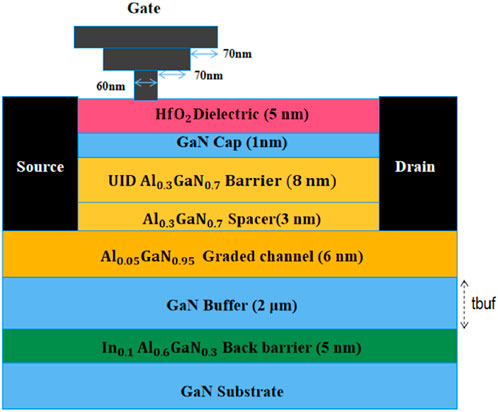
Figure 1. Schematic cross-sectional view of the proposed AlGaN coupled-channel MOS-HEMT featuring an InAlGaN back-barrier and an HfO2 gate dielectric.
The design prevents carrier spillover and improves 2DEG density and thermal performance. The gate structure uses a dual-tiered T-gate with a gate length of 60 nm and lateral extensions of 70 nm on each side. The gate-to-source and gate-to-drain distances are 0.1 μm and 0.3 μm, respectively. A short gate length and optimized gate area reduce parasitic capacitance and improve performance. The gate-to-drain distance (LGD) is larger than the gate-to-source distance (LSG) to maintain a lower electric field near the drain. This layout manages the electric field distribution by concentrating it near the gate and keeping it low at the source and drain, thereby reducing buffer leakage. It also improves breakdown voltage and high-frequency response (Russo and Di Carlo, 2007). The main structural parameters of the proposed MOS-HEMT are listed in Table 1.
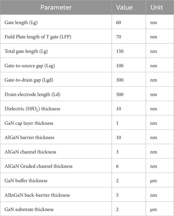
Table 1. Main parameters of proposed MOS-HEMT.
For device modelling, drift-diffusion and hydrodynamic transport models are used to analyses carrier mobility and velocity saturation. Thermal models handle self-heating effects, Shockley–Read–Hall recombination accounts for trap-assisted processes, polarization models simulate spontaneous and piezoelectric effects, and impact ionization models evaluate breakdown behavior. Additionally, high-resolution mesh refinement is applied around heterojunctions, gate edges, and contact regions to improve numerical accuracy for electric field and carrier transport simulations, ensuring reliable evaluation of device performance.
The band diagram corresponding to the proposed design is presented in Figure 2. The energy band diagram shows that the InAlGaN back-barrier and graded AlGaN channel enhance electron confinement and 2DEG density, while the high-k HfO2 gate dielectric improves electrostatic control and reduces leakage, leading to better device performance.
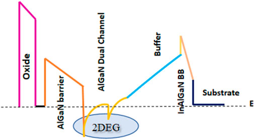
Figure 2. Conduction band diagram of the proposed coupled channel MOS-HEMT with the InAlGaN back-barrier.
The electrostatic potential distribution within the device is governed by the two-dimensional Poisson’s equation, which is expressed in Equation 1
where
where
The 2DEG sheet carrier density at the interface is determined by both electrostatic and polarization effects, is defined in Equation 4
where
with
The threshold voltage of the device incorporates the effects of work function difference, oxide and interface trap charges, and polarization charge, is expressed in Equation 6
where
In the linear regime, the drain current is described by Equation 7
where
The small-signal transconductance, which measures the sensitivity of the drain current to the gate voltage, is defined in Equation 8
and the cut-off frequency, which characterizes high-frequency response, is given by Equation 9
3 Result and discussion
The performance of the proposed coupled-channel (CC) MOS-HEMT structure, incorporating a high-k HfO2 dielectric and a lattice-matched InAlGaN back-barrier, has been comprehensively evaluated with a focus on both DC and RF characteristics. The transfer characteristics and transconductance responses are shown in Figures 3, 4, respectively, under a constant drain bias of 6 V. For performance benchmarking, these results are compared with those of the conventional composite-channel HEMT structure. The proposed structure demonstrates significant improvements, achieving a peak drain current of 1.19 A/mm and a maximum transconductance of 400 mS/mm.
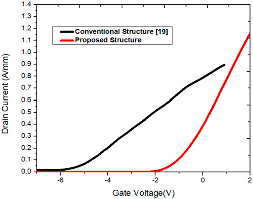
Figure 3. Transfer characteristics comparison, showing that the proposed coupled-channel InAlGaN BB MOS-HEMT achieves a higher drain current (1.19 A/mm) than the conventional HEMT, owing to enhanced carrier confinement.
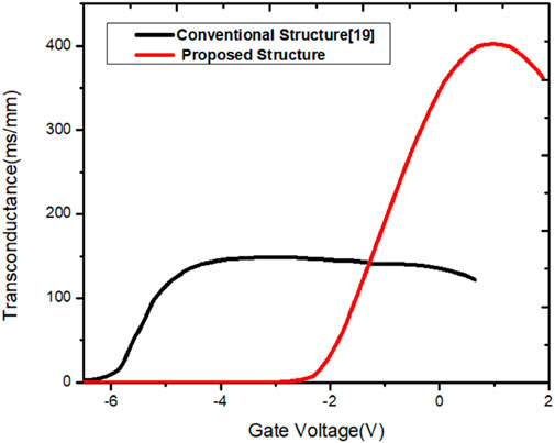
Figure 4. Comparison of transconductance (gm) characteristics between the proposed AlGaN coupled-channel InAlGaN BB MOS-HEMT and the conventional composite-channel HEMT, showing a peak gm of 400 mS/mm for the proposed device, indicating enhanced channel modulation.
Figure 5 presents the simulated output characteristics of the proposed device with the gate biased at 1 V. The results indicate a significant enhancement in drain current drivability and overall output performance compared to the conventional design. This improvement arises from the implementation of a graded Al0.05Ga0.95N coupled channel, which effectively reduces electric field degradation at the source/drain terminals and facilitates efficient carrier transport. The compositional grading introduces a polarization gradient that stabilizes the two-dimensional electron gas (2DEG) density, thereby enhancing current conduction and improving channel control. Furthermore, the incorporation of an In0.1Al0.6Ga0.3N back-barrier between the GaN buffer and substrate plays a crucial role in suppressing buffer leakage and strengthening carrier confinement by elevating the conduction band at the GaN/InAlGaN interface.
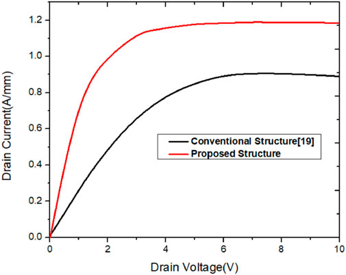
Figure 5. Simulated output characteristics of the proposed MOS-HEMT at Vgs = 1 V. The device shows better current saturation and higher output current compared to conventional design.
The incorporation of HfO2 as the gate dielectric offers several significant advantages for device performance. It enhances charge confinement at the gate-channel interface, minimizes gate leakage, and induces a positive shift in the threshold voltage. Owing to its high dielectric constant, HfO2 improves gate electrostatics, leading to better control over channel modulation and an enhanced subthreshold slope. Additionally, the introduction of an InAlGaN back-barrier increases the conduction band offset within the channel region, thereby reducing the surface 2DEG density and contributing further to a more positive threshold voltage.
The polarization-induced charge at various heterojunctions is highly dependent on the material composition. As illustrated, increasing the aluminum (Al) content in the AlGaN barrier enhances polarization charge and improves the 2DEG density up to an optimal limit. However, exceeding an Al composition of approximately 40% can introduce trap states that negatively impact RF performance, while concentrations below 15% may fail to generate sufficient polarization for robust 2DEG formation. In this study, the Al mole fraction has been carefully optimized within this suitable range to achieve reliable device operation, stronger electron confinement, and improved overall performance.
The simulated 2DEG concentration, shown in Figure 6, reaches approximately 1019 cm-3 without intentional doping, validating the effectiveness of polarization-induced charge accumulation. The presence of the InAlGaN back-barrier is shown to increase the electron density compared to the structure without it. Positive polarization charge at the AlGaN/GaN interface promotes electron accumulation, while the negative charge at the GaN/InAlGaN interface enhances confinement and suppresses parasitic channel formation. This dual-polarization effect is key to achieving high current drive and minimizing leakage.
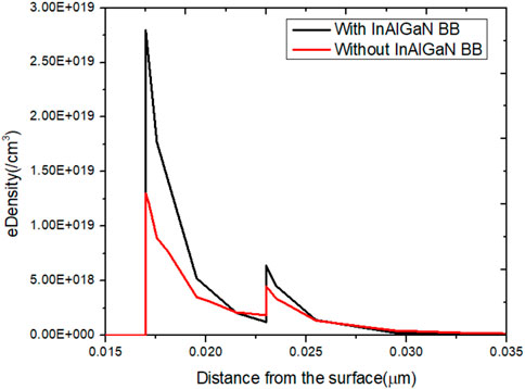
Figure 6. Electron concentration diagram of Proposed AlGaN coupled channel MOS-HEMT with and without InAlGaN BB-HEMT.
Figures 7a,b illustrate the conduction band profile and electron density distribution for three distinct InAlGaN compositions. The spontaneous polarization fields within lattice-matched
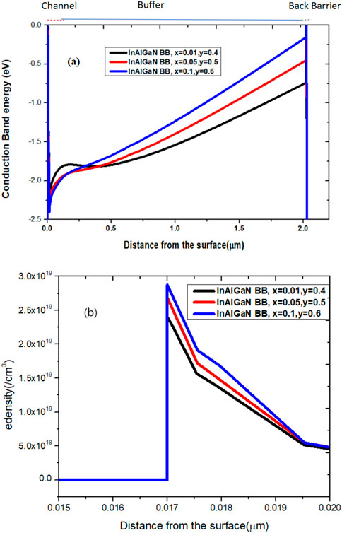
Figure 7. (a) Conduction band profile and (b) electron concentration distribution in the major channel of the AlGaN coupled-channel MOS-HEMT with an InAlGaN back-barrier (BB), showing the effect of indium (In) and aluminum (Al) mole fraction variation.
The corresponding transfer and transconductance characteristics for the three InAlGaN compositions are shown in Figures 8a,b, demonstrating that increasing indium and aluminum content enhances both drain current and transconductance due to stronger channel confinement under different mole fractions.
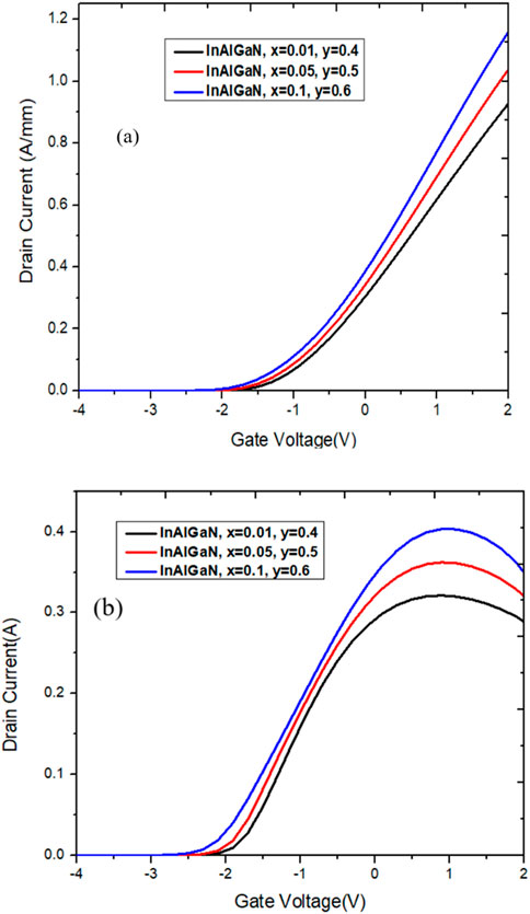
Figure 8. (a) Transfer and (b) Transconductance profiles for InAlGaN BB-HEMT devices with mole fraction variation, measured at a drain-source voltage of 6 V.
Figures 9a,b illustrate the impact of back-barrier thickness on device characteristics, with evaluations performed at Lg = 60 nm and Vds = 6 V. As the back-barrier thickness increases, a noticeable negative shift in the threshold voltage is observed, accompanied by an increase in transconductance from 300 mS/mm to 400 mS/mm. This behavior arises from the gradual modulation of the conduction band, which stabilizes the sheet charge distribution. The device exhibits optimal DC performance at a channel thickness below 5 nm, where the maximum drain current increases from 0.94 A/mm to 1.19 A/mm.
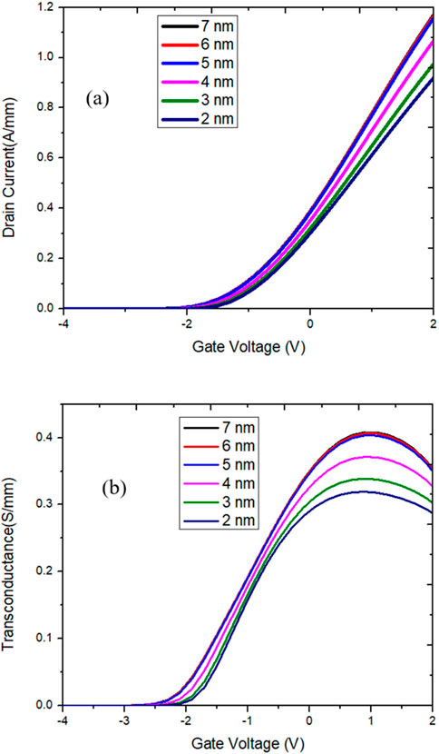
Figure 9. (a) Transfer and (b) Transconductance profiles for InAlGaN BB-HEMT with different back barrier layer thickness measured at a drain-source voltage of 6 V.
Based on the initial simulation results both the maximum drain current and transconductance improve as the InAlGaN back-barrier thickness varies from 2 nm to 5 nm. However, beyond 5 nm, there is no significant enhancement in device characteristics, as shown in the graph. This saturation occurs because, at approximately 5 nm, the conduction band offset and vertical carrier confinement reach their optimum, leading to a well-confined two-dimensional electron gas. Increasing the thickness beyond this point does not further enhance 2DEG density or carrier transport. Moreover, excessively thick back-barrier layers slightly increase parasitic capacitance, which may degrade the device’s high-frequency performance.
Figure 10 shows the effect of GaN buffer thickness on the proposed device. As tbuf decreases from 3.0 µm to 2.0 µm, stronger back-barrier coupling enhances 2DEG confinement, resulting in higher Ion, improved transconductance and reduced DIBL. However, further reducing tbuf below 2.0 µm, stronger trap-channel interactions, increases leakage and reduced breakdown voltage. Therefore, 2.0 µm was selected as the optimum thickness, balancing performance improvement and device reliability.
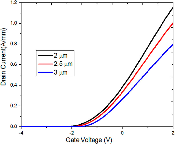
Figure 10. Effect of GaN buffer thickness (tbuf) on device performance. Thinner buffers enhance back-barrier control and improve Ion and transconductance but also increase leakage current.
The electric field distribution along the channel is illustrated in Figure 11. In the conventional single-channel configuration, the peak electric field reaches approximately 3 MV/cm near the gate region, which can lead to increased scattering and leakage. In contrast, the proposed graded AlGaN coupled-channel configuration significantly modifies the electric field profile by enhancing the field between the source and gate, thereby enabling smoother band bending. Furthermore, the integration of a field plate with the double-channel architecture effectively redistributes the electric field, leading to improved 2DEG confinement and a higher 2DEG density. This optimized field management not only minimizes interface scattering and leakage but also enhances carrier transport efficiency, demonstrating the novelty and performance advantage of the proposed device over conventional structures.
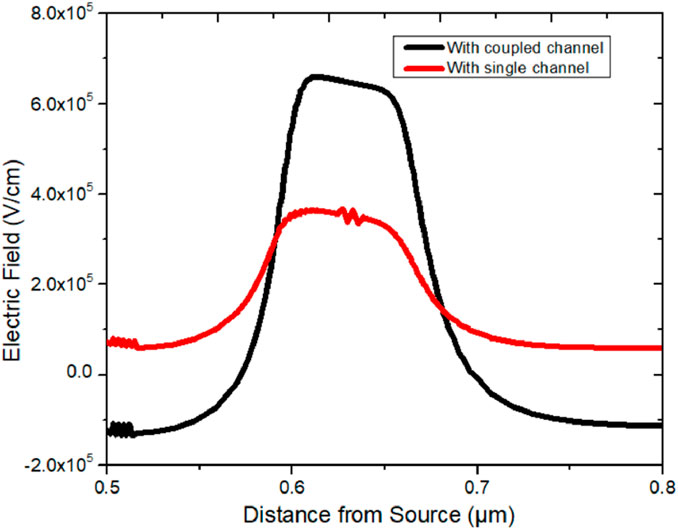
Figure 11. Electric field distribution along the source-to-drain direction, comparing cases with and without the coupled-channel.
Figure 12 illustrates the variation of threshold voltage (Vth) as a function of HfO2 dielectric thickness. A notable positive shift of up to −2 V is observed when the oxide thickness is scaled down to 5 nm, which can be attributed to improved electrostatic control and suppression of interface trap effects. To evaluate the high-frequency performance of the proposed device, small-signal intrinsic capacitances were extracted. Figure 13 shows the variation of total gate capacitance (Cgg) across a gate voltage sweep from −4 V to +4 V. The proposed HEMT demonstrates a Cgg of approximately 0.5 pF, primarily due to the reduced gate length and minimized buffer charge. This lower gate capacitance, combined with enhanced transconductance, contributes to improved switching speed and superior overall high-frequency performance.
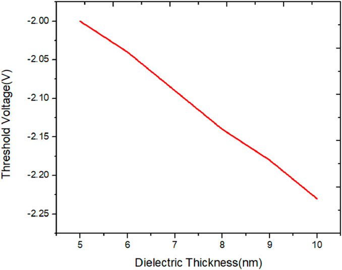
Figure 12. Threshold voltage variation as a function of high-k oxide thickness, showing a positive shift with decreasing dielectric thickness.
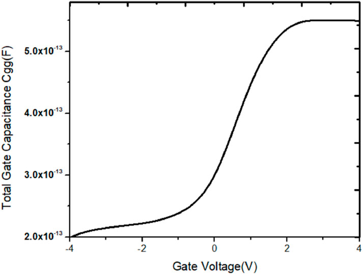
Figure 13. Total gate capacitance (Cgg) as a function of gate voltage.
Figures 14a,b present the gain and frequency characteristics of the proposed device, highlighting its superior high-frequency performance. A significant enhancement in both the cut-off frequency (fT) and the maximum frequency of oscillation (fmax) is observed, demonstrating the device strong potential for RF and high-speed applications. These improvements are primarily attributed to the reduced total gate capacitance (Cgg), efficient channel modulation, and optimized electric field distribution enabled by the proposed structure. Furthermore, Figure 15 compares the frequency characteristics (fT and fmax) of the proposed InAlGaN back-barrier coupled-channel MOS-HEMT with previously reported reference structures, including the composite-channel HEMT (Liu et al., 2005), dual-channel HEMT (Chu et al., 2005), double-channel HEMT with back-barrier (Kamath et al., 2012), AlInGaN/InGaN/GaN DHFET (Adivarahan et al., 2008), and the graded AlGaN back-barrier HEMT (Zhang et al., 2025). The proposed device shows superior performance due to enhanced 2DEG confinement and improved carrier transport. Table 2 provides a comprehensive comparison of the DC performance metrics for various GaN HEMT architectures employing graded back-barriers. The results clearly highlight the proposed design’s advantages, including improved drain current, higher transconductance, and superior frequency response, demonstrating its effectiveness for next-generation high-frequency electronic applications.
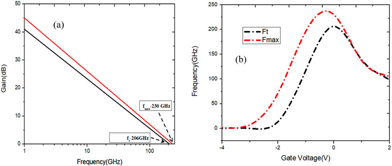
Figure 14. (a) Frequency-dependent gain profile of the proposed device. (b) Variation of cut-off and maximum frequencies for the MOS-HEMT as the gate voltage is swept from negative to positive, with the drain Voltage held constant at 6 V.
![Scatter plot showing frequency in gigahertz on the y-axis, comparing multiple works labeled [19], [20], [21], [22], [24], [25], and Proposed Work on the x-axis. Black squares represent \(f_t\) and red circles represent \(f_{\text{max}}\). Data points cluster between 0 and 250 GHz, with Proposed Work reaching highest values.](https://www.frontiersin.org/files/Articles/1666203/fmats-12-1666203-HTML/image_m/fmats-12-1666203-g015.jpg)
Figure 15. Comparison of ft, fmax of several graded back barrier structure from literature.
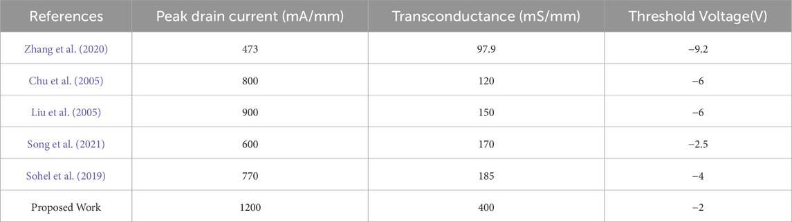
Table 2. Comparison of device performance parameters with previously reported coupled-channel MOS HEMT designs.
The implementation of a Tired T-gated structure with a field plate further improves the breakdown voltage, as shown in Figure 16. Simulations were performed with varying field plate lengths (70, 80, and 90 nm), showing that larger plates better redistribute the electric field and suppress gate-drain tunneling.The standard gate structure achieved a breakdown voltage of 604 V, while the T-gated device with a 90 nm field plate exhibited a significantly improved breakdown of 640 V.
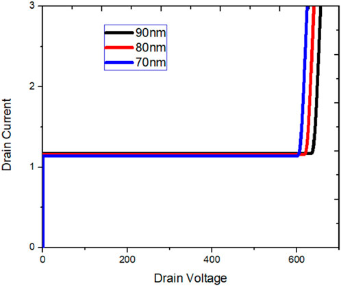
Figure 16. The influence of field plate length in a Tired T-gated structure on the breakdown voltage. The device is analyzed with simulations incorporating various field plate deck length (70, 80, and 90 nm).
4 Conclusion
The comprehensive simulation-based investigation of the proposed AlGaN Coupled-Channel MOS-HEMT, incorporating an InAlGaN back-barrier and high-k HfO2 dielectric, demonstrates significant performance enhancements tailored for millimeter-wave and high-power electronic applications. The integration of a graded AlGaN coupled channel structure results in enhanced carrier transport and improved current drivability compared to conventional AlGaN CC-HEMT architectures. The engineered InAlGaN back-barrier effectively suppresses parasitic channel formation beneath the 2DEG by enhancing carrier confinement, thereby minimizing leakage and ensuring robust electrostatic control. Key performance metrics include a peak drain current of 1.19 A/mm, a maximum transconductance of 400 mS/mm, and a low specific on-resistance of 0.106 Ωmm, along with a high breakdown voltage of 640 V achieved via an optimized double-layer T-gate field plate configuration. Furthermore, the incorporation of a 5 nm HfO2 gate dielectric facilitates a favorable positive shift in threshold voltage (up to −2 V) and contributes to improved gate control. High-frequency characteristics are evidenced by a cut-off frequency (ft) of 206 GHz at a 60 nm gate length, attributed to the elevated transconductance and reduced total capacitance. Overall, the proposed structure offers a balanced trade-off between high current density and high-frequency response and the breakdown characteristics, establishing it as a strong candidate for next-generation RF power amplifiers and high-performance switching devices.
Data availability statement
The original contributions presented in the study are included in the article/supplementary material, further inquiries can be directed to the corresponding author.
Author contributions
LK: Writing – original draft, Writing – review and editing. KS: Writing – original draft, Writing – review and editing.
Funding
The author(s) declare that no financial support was received for the research and/or publication of this article.
Conflict of interest
The authors declare that the research was conducted in the absence of any commercial or financial relationships that could be construed as a potential conflict of interest.
Generative AI statement
The author(s) declare that no Generative AI was used in the creation of this manuscript.
Any alternative text (alt text) provided alongside figures in this article has been generated by Frontiers with the support of artificial intelligence and reasonable efforts have been made to ensure accuracy, including review by the authors wherever possible. If you identify any issues, please contact us.
Publisher’s note
All claims expressed in this article are solely those of the authors and do not necessarily represent those of their affiliated organizations, or those of the publisher, the editors and the reviewers. Any product that may be evaluated in this article, or claim that may be made by its manufacturer, is not guaranteed or endorsed by the publisher.
References
Abderrahim, Y., Hichem, B., Lamir, S., and Amir, A. M. (2018). “Role of High-K and gate engineering in improving Rf/analog performances of in 0.2 Ga0. 8As/Al0. 3Ga0. 7As HEMT,” in 2018 international conference on communications and electrical engineering (ICCEE) (IEEE), 1–4. doi:10.1109/CCEE.2018.8634517
Adivarahan, V., Gaevski, M. E., Islam, M. M., Zhang, B., Deng, Y., and Khan, M. A. (2008). Double-recessed high-frequency AlInGaN/InGaN/GaN metal–oxide double heterostructure field-effect transistors. IEEE Trans. Electron Devices 55 (2), 495–499. doi:10.1109/TED.2007.913001
Chow, T. P., and Tyagi, R. (1994). Wide bandgap compound semiconductors for superior high-voltage unipolar power devices. IEEE Trans. Electron Devices 41 (8), 1481–1483. doi:10.1109/16.297751
Chu, R., Zhou, Y., Liu, J., Wang, D., Chen, K., and Lau, K. (2005). AlGaN-GaN double-channel HEMTs. IEEE Trans. Electron Devices 52 (3), 438–446. doi:10.1109/TED.2005.844791
Del Alamo, J. A. (2011). Nanometre-scale electronics with III–V compound semiconductors. Nature 479, 317–323. doi:10.1038/nature10677
Dubey, S. K., and Islam, A. (2024). High-k HfO2 influence on AlGaN/GaN MOSHEMTs for RF system applications. Microsyst. Technol. 30, 163–175. doi:10.1007/s00542-023-05576-w
Fletcher, A. S. A., and Nirmal, D. (2017). A survey of Gallium Nitride HEMT for RF and high power applications. Superlattices Microstruct. 109, 519–537. doi:10.1016/j.spmi.2017.05.042
Fletcher, A. S. A., Nirmal, D., Ajayan, J., Arivazhagan, L., Hamza, K. H., and Murugapandiyan, P. (2022). 60 GHz double deck T-Gate AlN/GaN/AlGaN HEMT for V-Band satellites. Silicon 14, 5941–5949. doi:10.1007/s12633-021-01367-y
Kalita, S., Awadhiya, B., and Changmai, P. (2023). Performance analysis of gallium nitride-based DH-HEMT with polarization-graded AlGaN back-barrier layer. Appl. Phys. B 129, 98. doi:10.1007/s00340-023-08042-7
Kamath, A., Patil, T., Adari, R., Bhattacharya, I., Ganguly, S., Aldhaheri, R. W., et al. (2012). Double-Channel AlGaN/GaN high electron mobility transistor with back barriers. IEEE Electron Device Lett. 33 (12), 1690–1692. doi:10.1109/LED.2012.2218272
Kim, J. G., Kang, S. H., Janicki, Ł., Lee, J. H., Ju, J. M., Kim, K. W., et al. (2019). Growth of AlGaN/GaN heterostructure with lattice-matched AlIn(Ga)N back barrier. Solid-State Electron. 152, 24–28. doi:10.1016/j.sse.2018.11.002
Liu, J., Zhou, Y., Chu, R., Yong Cai, , Chen, K., and Lau, K. (2005). Realization of linearity in composite-channel HEMTs using Al0.3Ga0.7N–Al0.05Ga0.95N–GaN layers. IEEE Electron Device Lett. 26 (2), 145–147. doi:10.1109/LED.2005.843218
Murugapandiyan, P., Rajya Lakshmi, V., Wasim, M., and Meenakshi Sundaram, K. (2019). Investigation of ultra-scaled AlN/GaN/InGaN double heterojunction HEMT for high-frequency applications. Int. J. Electron. Lett. 8, 472–482. doi:10.1080/21681724.2019.1636295
Noual, A., Zitouni, M., Touati, Z. E., Saidani, O., and Yousfi, A. (2023). Numerical Study of T-gate AlGaN/AlInGaN/GaN moshemt with single and double barrier for thz frequency applications. East Eur. J. Phys. (4), 216–225. doi:10.26565/2312-4334-2023-4-27
Piotrowicz, S., Jacquet, J. C., Gamarra, P., Patard, O., Dua, C., Chartier, E., et al. (2018). InAlGaN/GaN with AlGaN back-barrier HEMT technology on SiC for Ka-band applications. Int. J. Microw. Wirel. Technol. 10 (1), 39–46. doi:10.1017/S175907871700112X
Russo, S., and Di Carlo, A. (2007). Influence of the source–gate distance on the AlGaN/GaN HEMT performance. IEEE Trans. Electron Devices 54 (5), 1071–1075. doi:10.1109/TED.2007.894614
Sandeep, V., and Pravin, J. C. (2021). Influence of Graded AlGaN sub-channel over the DC and Breakdown characteristics of a T-gated AlGaN/GaN/AlInN MOS-HEMT. Superlattices Microstruct. 156, 106954. doi:10.1016/j.spmi.2021.106954
Sohel, S. H., Xie, A., Beam, E., Xue, H., Razzak, T., Bajaj, S., et al. (2019). Polarization engineering of AlGaN/GaN HEMT with graded InGaN sub-channel for high-linearity X-Band applications. IEEE Electron Device Lett. 40 (4), 522–525. doi:10.1109/LED.2019.2899100
Song, W., Zheng, Z., Chen, T., Wei, J., Yuan, L., and Chen, K. J. (2021). RF linearity enhancement of gan-on-si HEMTs with a closely coupled double-channel structure. IEEE Electron Device Lett. 42 (7), 1116–1119. doi:10.1109/LED.2021.3087785
Teo, K. H., Zhang, Y., Chowdhury, N., Rakheja, S., Ma, R., Xie, Q., et al. (2021). Emerging GaN technologies for power, RF, digital, and quantum computing applications: recent advances and prospects. J. Appl. Phys. 130, 160902. doi:10.1063/5.0061555
Upadhyay, K. T., and Chattopadhyay, M. K. (2019). I-V model for AlInGaN/GaN HEMTs considering compositional and thickness variations. Mater. Today Proc. doi:10.1016/j.matpr.2019.06.700
Wang, H. L., Yang, P., Xu, K., Duan, X. Y., and Sun, S. X. (2019). The AlInGaN back barrier effect on DC characteristics of AlGaN/GaN high electron mobility transistor. Int. J. Mod. Phys. B 33, 1950190. doi:10.1142/S021797921950190X
Yue, Y., Hao, Y., Zhang, J., Ni, J., Mao, W., Feng, Q., et al. (2008). Enhanced performance of AlGaN/GaN MOS-HEMTs using HfO2 dielectric and Al2O3 passivation via ALD. IEEE Electron Device Lett. 29 (8), 838–840. doi:10.1109/LED.2008.2000949
Zhang, Y., Li, Y., Wang, J., Shen, Y., Du, L., et al. (2020). High-Performance AlGaN double channel HEMTs with improved drain Current density and high breakdown voltage. Nanoscale Res. Lett. 15, 114. doi:10.1186/s11671-020-03345-6
Keywords: AlGaN/GaN, MOSHEMT, InAlGaN back barrier, coupled channel, HfO2 dielectric
Citation: K LP and S K (2025) Influence of polarization engineering in
Received: 15 July 2025; Accepted: 12 September 2025;
Published: 10 October 2025.
Edited by:
Leszek A. Majewski, The University of Manchester, United KingdomReviewed by:
Yousfi Abderrahim, Universite Mohamed El Bachir El Ibrahimi de Bordj Bou Arreridj, AlgeriaAdam Szyszka, Wrocław University of Technology, Poland
Copyright © 2025 K and S. This is an open-access article distributed under the terms of the Creative Commons Attribution License (CC BY). The use, distribution or reproduction in other forums is permitted, provided the original author(s) and the copyright owner(s) are credited and that the original publication in this journal is cited, in accordance with accepted academic practice. No use, distribution or reproduction is permitted which does not comply with these terms.
*Correspondence: Lakshmi Priya K., bGs0ODk5QHNybWlzdC5lZHUuaW4=