 JianJun Yang
 ShuangShuang Shao1,2
 Chi Feng
- 1College of Electron and Information, University of Electronic Science and Technology of China, Zhongshan Institute, Zhongshan, China
- 2School of Optoelectronic Science and Engineering, University of Electronic Science and Technology of China, Chengdu, China
A large-scale growth of zinc oxide (ZnO) nanorod arrays on graphene sheets was fabricated by a hydrothermal technique, and the Fowler–Nordheim theory was used to build a model to describe the properties of the arrays’ field emission. The results indicated that the morphological characteristics of the ZnO nanorods grown on the graphene sheets can be easily tuned by varying the reaction time and concentrations of the reaction solution. The regular ordered ZnO nanorods arrays on the graphene sheets were obtained under the appropriate experimental conditions. Further, this composite cathode was demonstrated to possess excellent field emission properties due to the outstanding mechanical and electrical properties of graphene. The field emission current density of the composite cathode reached 1,448 μA cm–2 at the electric field of 16.5 V μm–1. The key parameter, field enhancement factor, reached 6,366, while the pure graphene cathode field is about 1,660. These specific nanorod arrays with enhancement of the field emission properties would be useful to sensor or modulator units for accessing networks.
Introduction
Graphene is usually used as a single cathode field emission material due to its excellent properties, such as the perfect quantum tunneling effect, excellent electrical conductivity, and mechanical properties [1]. It can also form sharp edges and concaves which can obtain a larger field enhancement factor. All of these made it possible to have the excellent field emission properties [2, 3]. It is advantageous for electron tunneling, and its two-dimensional conductive surface has the advantage in larger current [4–6]. Therefore, graphene can be used as a kind of field emission cathode material [4–8]. However, the emission performance of the graphene cathode field and the stability of the emission are still need to be solved urgently. The sharpness of the ground of graphene prepared by the chemical vapor deposition (CVD) method was limited due to the choice of flat copper or nickel as the substrate, which also limited the field emission properties [9–12].
ZnO nanorods with a wide bandgap (3.2eV) are good candidates for use in next-generation electronics and optoelectronics [13–17]. Zinc oxide/graphene hybrids have excellent emitting behavior characteristic, which is suitable for application in the field emission technology [18, 19]. Raman spectroscopy has figured out many excellent properties of graphene layers [20–23]. Therefore, the compound of graphene sheets with ZnO nanorods had recently been reported for multifunctional applications, such as gas sensors, light-emitting diodes, and solar cells [24–30].
So far, there was seldom report on the transfer of graphene sheets onto the silicon substrate with the silica film by wet transfer and the growth of ZnO nanorods on the graphene sheets. In this study, the two-step method was used to prepare ZnO nanorods on the surface of graphene, and the effect of the experimental conditions on the morphology of the ZnO nanostructure had been studied. The field emission properties of such ZnO nanorod/graphene cathodes have been described by a model and been tested.
Principle
As we know, the expression of the field emission current density is as follows, based on Fowler–Nordheim theory (F–N equation):
where J is the current density and F is the local field strength of the cathode surface; A and B are constants with the value of 1.54 × 10⁻⁶ and 6.87 × 10⁷, respectively; ϕ is the work function; and y represents 3.79 × 10⁻⁴ × E1/2/ϕ, v(y) = (0.95 – y2), where E is the applied field strength. And, t2 has a value close to 1.1.
Considering that the field emission cathode is usually with a special shape, the field enhancement factor (β) is introduced into the expression Eq. 1, and F can be expressed by β × E. And, Eq. 1 can be transformed as follows:
It can be used as a basis to illustrate the field emission mechanism with a synthesized cathode. The field emission properties can be described by ln (J/E2) – (1/E) curve. And, the field enhancement factor can be obtained according to the curve slope.
Materials and Methods
Materials
Copper foil (Cu) was purchased from Xiamen Xicheng Graphene Technology Co., Ltd., acetone (CH3COCH3, ≥99.5%) and isopropyl alcohol (C3H8O, 99.7%) were purchased from Zhongshan Jingke Chemical Instrument Co., Ltd., silica wafer (SiO2/Si, 300 nm) was purchased from Harbin Tebo Technology Co., Ltd., and poly (methyl methacrylate) (PMMA, 60 mg/ml) was purchased from Sigma-Aldrich (Shanghai) Trading Co., Ltd. Methane (CH4), hydrogen (H2), and argon (Ar) were purchased from Zhongshan Fu'an Gas Co., Ltd. The ZnO sol–gels consist mainly of three kinds of materials, zinc acetate, ethanolamine, and ethanol. Zinc acetate (Zn (CH3COO)2, 99.99%) and ethanolamine (C2H7NO, ≥99.0%) were purchased from Shanghai Aladdin Biochemical Technology Co., Ltd. Ethanol absolute (CH3CH2OH, ≥99.7%) was purchased from Zhongshan Jingke Chemical Instrument Co., Ltd. Zinc nitrate hexahydrate (Zn(NO3)2•6H2O, 99.998%) and hexamethylenetetramine (C6H12N4, ≥99.5%) were purchased from Shanghai Aladdin Biochemical Technology Co., Ltd.
Method
Synthesis of Graphene Sheets
Graphene sheets were synthesized on the Cu substrate by chemical vapor deposition (CVD). Cu foils (40 × 25 × 0.1 mm3) were washed with a mixed solvent of acetone, isopropyl alcohol, and deionized water by ultrasonic cleaning. Copper foil was loaded in the CVD quartz tube with the pressure of below 1.1 Pa and heated at 1,030°C for 65 min in hydrogen without changing the flowing rate. Then, the mixture of gases (H2:CH4) with the flowing rate ratio of 50:1 was introduced into the flow as the carbon source for 20 min. After reaction, the quartz tube was dropped to room temperature. The sample was removed from a tube furnace.
Transfer of Graphene Sheets
The transfer process was based on the utilization of the poly (methyl methacrylate) (PMMA) film as a mediator. PMMA was spin-coated on the surface of graphene sheets with the Cu substrate. After baking at 140°C for 10 min, the organic solvent was removed from PMMA. The sample was placed in a 30-mg/ml ammonium persulfate solution for etching to strip the copper foil. After etching, PMMA/graphene sheets were moved into a beaker containing deionized water and transferred onto the silicon substrate and dried at room temperature. Then, the sample was baked at 120°C for an hour. Finally, the sample was soaked in an acetone solution at 50°C to remove PMMA, and then washed with isopropyl alcohol.
Preparation of ZnO Nanorods/Graphene Composite Film
A certain amount of zinc nitrate hexahydrate and hexamethylenetetramine was mixed in water as the reactant solution. ZnO sol–gel as a ZnO seed layer was spin-coated onto the graphene sheets and transferred onto the silicon substrate. Then, the samples were placed in a reaction kettle with a reactant solution at 95°C for the suitable time for the growth of ZnO nanorods through a hydrothermal method, followed by natural cooling to room temperature and washed with deionized water for several times and dried at room temperature. The morphological characteristics of the ZnO nanorods grown on the graphene sheets were investigated at different reaction solution concentrations and temperatures.
A schematic diagram of the fabrication process is illustrated in Figure 1.
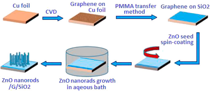
FIGURE 1. Schematic of the fabrication process of the graphene/ZnO composite film.
Field Emission Measurement
The field emission properties were measured by using a parallel plate electrode configuration. The sample was fixed on a stainless stage with a conductive tape as the cathode, and a copper electrode with the bottom diameter of 2 mm was used as an anode. The field emission measurement needed a vacuum below 2 × 10⁻⁴ Pa. The emission current was measured at voltages ranging from 100 to 5000 V. The spacing between the anode and the cathode was maintained at 300 μm.
Results and Discussions
Figure 2 shows the Raman spectrum of the graphene sheets transferred onto the silicon substrate (Figure 2A), and the optical image (Figure 2B) and SEM images of the graphene film onto the copper substrate (Figure 2C) and silicon substrate (Figure 2D), respectively. Figures 2B and 2D are photos of the graphene sheets on the silicon substrate and local magnification, respectively.
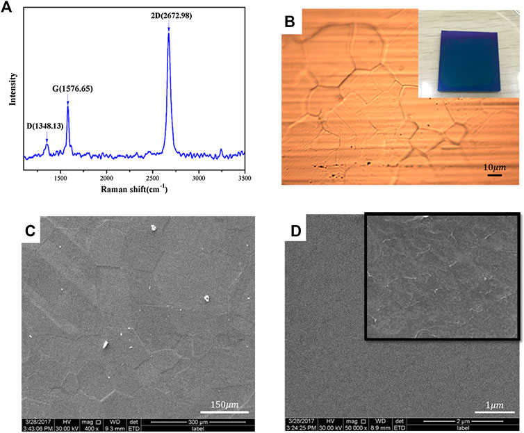
FIGURE 2. Raman spectrum of graphene transferred onto the silicon substrate (A) and the optical microscope image of copper-based graphene (B) and SEM images of copper-based graphene (C) and the flattened graphene transferred onto the SiO2/Si substrate (D).
Raman spectroscopy is a promising method for inspecting the ordered/disordered crystal structures of carbonaceous materials and the different layer characteristics of graphene. From Figure 2A, it is observed that the Raman spectrum of graphene exhibited the D peak at 1,348.31°cm−1, the G peak at 1,576.65°cm−1, and the 2D peak at 2,672.98°cm−1. The intensity of D peak was very small, indicating that the local defects and disorder of graphene transferred onto the silicon substrate were little. The number of layers of graphene can be determined by the peak intensity ratio of the G peak to that of the 2D peak of the Raman spectrum [20–23]. For our sample, the peak intensity ratio of the G peak to that of the 2D peak was approximately 2, indicating that graphene is a monolayer [20]. The distribution of grain and grain boundary of graphene on the copper substrate was observed in the optical image (Figures 2B,C). The color of the graphene film transferred onto the silicon substrate was dark blue (inserted in Figure 2B). The graphene sheets on the copper substrate were flat. However, the wrinkles of graphene sheets on the silicon substrate were observed (Figure 2D). The edge of the graphene film would be rolled up when transferring. And there would be “fracture” resulting in an incomplete film due to the softness of the copper foil. It was inevitable that the transfer process causes the graphene sheets to be wrinkled because of the soft monolayer structure. In addition, the surface of graphene will absorb impurities during the transfer.
ZnO nanorod arrays on graphene sheets were obtained through hydrothermal routes. Figure 3 shows the XRD patterns of the ZnO nanorod arrays on graphene sheets and the pure graphene, respectively. A diffraction peak of the pure graphene near 2θ value of 26.4° was observed in Figure 3. There was a strong diffraction peak in the vicinity of 2θ value of 31.8°, corresponding to the diffraction peak of the wurtzite-type zinc oxide (100) crystal plane. There were also some diffraction peaks near 34.4°, 36.3°, and 56.6°, corresponding to zinc oxide with crystal planes of (002), (101), and (110). The comparison between ZnO and the composite films in Figure 3B shows that there were some other diffraction peaks except the diffraction peaks in about the same position as those in Figure 3A, but the intensity was relatively small, indicating the quality of the composite film was better.
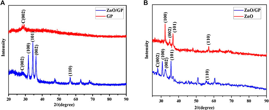
FIGURE 3. XRD spectra of graphene and graphene/ZnO nanorods (A). ZnO and graphene/ZnO nanorods (B).
To observe the growth of the ZnO nanorods on the graphene sheets, SEM images were taken, as shown in Figures 4 and 5. Figure 4 shows SEM images of the ZnO nanorods on the graphene sheets with zinc nitrate hexahydrate of 10 mM (Figure 4A), 15 mM (Figure 4B), and 25 mM (Figure 4C), respectively, for 5 h. Figure 4D is the local magnification of Figure 4C. The density and diameter and size of ZnO nanorods increased with increasing of the reaction solution concentration. When the reaction solution concentration was 25 mM, the uniform ZnO nanorods were successfully grown on the graphene surface, and the order of ZnO nanorod arrays could be obtained. The average length and diameter of ZnO nanorods is 2 μm and 200 nm, respectively. The hexagonal structure of ZnO naorods can be clearly seen from Figure 4D.
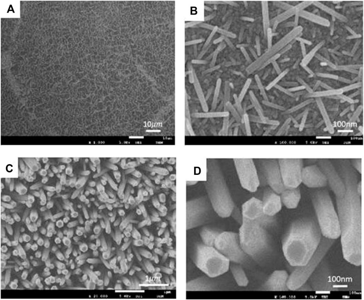
FIGURE 4. SEM images of the ZnO nanorods on the graphene sheets with zinc nitrate hexahydrate of 10 mM (A), 15 mM (B), and 25 mM (C), respectively, for 5 h.
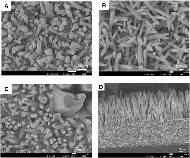
FIGURE 5. SEM images of the ZnO nanorods on the graphene sheets with zinc nitrate hexahydrate of 25 mM and the reaction time of 3 h (A), 4 h (B), and 5 h (C), respectively.
Figure 5 shows the SEM images of the ZnO nanorods on the graphene sheets with zinc nitrate hexahydrate of 25 mM and the reaction time of 3 h (Figure 5A), 4 h (Figure 5B), and 5 h (Figure 5C), respectively. The inset in Figure 5C is the local amplification and the sectional drawing of the sample (Figure 5D). It can be seen that the density and diameter and size and order of ZnO nanorods increased with increasing of the reaction time. The ZnO seed layer was preferably the growth of the c-axis–oriented ZnO nanostructures [26]. The formation of ZnO was a process of increasing the entropy from a chemical point of view [30]. The adhesion of hexamethylenetetramine (HMTA) to the nonpolar surface accelerated the growth of the crystal in the [0001] direction and slowly hydrolyzed HCHO and NH3 in the solution. All were beneficial to the orientation growth of ZnO nanorods to obtain longer arrays.
To analyze the field emission performance, the curves of field emission current density on the applied electric field (J–E) from graphene/ZnO nanorods based on CVD were plotted. Emission current density vs. electric field curves and F–N plot at different emission cathodes are shown in Figures 6A and 6B, respectively. From Figure 6A, when the emission current density is 1 μA°cm–2, the turn-on field of graphene/ZnO nanorod composite films (4 V°μm–1) was obviously smaller than that of the pure graphene films (7 V°μm–1). The reason to the graphene film with larger turn-on field could be that there were fewer sharp edges and concaves in graphene by CVD, which led to the linear change of the current and the slow growth at the beginning of the applied electric filed. The field emission current density of the composite cathode could reach to 1,448 μA cm–2 when the electric field reaches 16.5 V μm–1 (Figure 6A). Further, from Figures 4B–D, with the increase of reactant concentration, the current density decreased and the emission performance became worse. Emission current density vs. electric field curves and F–N plot of graphene/ZnO nanorods at different concentrations of reactants were shown in Figures 7A and 7B, respectively. From Figure 7, it is observed that current density decreased and the emission performance became worse with the increase of the reactant concentration.
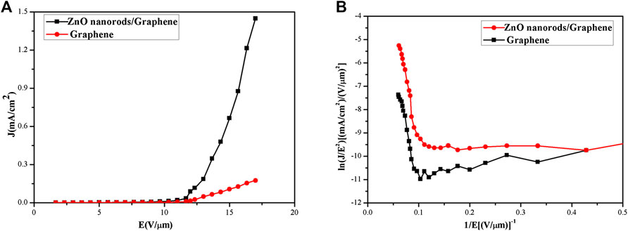
FIGURE 6. (A) Emission current density vs. electric field curves and (B) F–N plot at different emission cathodes.
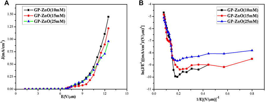
FIGURE 7. (A) Emission current density vs. electric field curves and (B) F–N plot of graphene/ZnO nanorods at different concentrations of reactant.
The field enhancement factor can be used to described the field emission effect of this synthesized cathode [31]. From the F–N equation model, the field enhancement factor of the graphene cathode field is about 1,660, and the field enhancement factor of the graphene/ZnO composite cathode field could reach 6,366. It can be indicated from the F–N equation model that the field enhancement factor was determined by the slope of the ln (J/E2) and (1/E) curves and the work function of the material. The work functions of graphene and zinc oxide are 5eV and 5.3eV, respectively [32]. Graphene/ZnO composites had a smaller work function than graphene or ZnO [33]. Therefore, the field enhancement factor of the composites was larger and the emission current density was higher, so the field emission performance was better.
Graphene had excellent electrical conductivity and electronic transport capability, which can form good ohmic contact with ZnO, and also improved the efficiency of electron transport. Therefore, the introduction of the graphene layer not only solved the contact problem between ZnO and the substrate but also promoted the transmission of electrons. In addition, the graphene films prepared by the CVD method mostly appeared as concaves. If the graphene film is deposited in a short time, there will be more defects and raised edges. And, they would be sharp at the edge after the wet transfer. Furthermore, the introduction of ZnO nanorods could make up for the defect of insufficient emission in the local area and obtained excellent field emission properties.
Conculsions
Graphene sheets were synthesized on the Cu substrate by chemical vapor deposition and transferred onto the silicon substrate with poly (methyl methacrylate) (PMMA) as a mediator. Zinc oxide nanosructures grown on graphene sheets were prepared by the hydrothermal method. The results indicated that the morphological characteristics of the ZnO nanorods grown on the graphene sheets could be easily tuned by varying the reaction time and concentration of the reaction solution. With increasing of the reaction time and concentration of the reaction solution, the density and size of ZnO nanorods increased. The regular ordered ZnO nanorod arrays on the graphene sheets were obtained at the conditions of zinc nitrate hexahydrate of 10 mM for 5 h. The field emission current density of ZnO nanorods arrays/graphene composite cathode reached 1,448 μA cm–2 at the electric field of 16.5 V μm–1. The field enhancement factor of ZnO nanorod arrays/graphene composite cathode field reached 6,366, while the pure graphene cathode field is about 1,660. The enhancement of the field emission properties indicated that ZnO nanorods arrays/graphene had lower turn-on fields and threshold fields as well as higher field enhancement factors than pure graphene.
Data Availability Statement
The original contributions presented in the study are included in the article/Supplementary Material; further inquiries can be directed to the corresponding author.
Author Contributions
JY, YW, and JY and YW designed this project. SS, YL, and FC carried out most of the experiments and data analysis.
Funding
This work was sponsored by National Key R&D Program of China (Grant No. 2018YFB0407100) and supported by Zhongshan Innovative Research Team Program (180809162197886).
Conflict of Interest
The authors declare that the research was conducted in the absence of any commercial or financial relationships that could be construed as a potential conflict of interest.
Acknowledgments
This work was supported by the State Key Laboratory of Electronic Thin Films and Integrated Devices and Zhongshan division of the State Key Laboratory of Electronic Thin Films and Integrated Devices. And, we thank Jian Zhong for this work constructive comments.
References
1. Berger C, Song Z, Li X, Wu X, Brown N, Naud C, et al. Electronic confinement and coherence in patterned epitaxial graphene. Science. (2006). 312(5777):1191–6. doi:10.1126/science.1125925
2. Deng JH, Yu B, Li GZ, Hou XG, Zhao ML, Li DJ, et al. Self-assembled growth of multi-layer graphene on planar and nano-structured substrates and its field emission properties. Nanoscale. (2013). 5:12388–93. doi:10.1039/c3nr04145j
3. Wang BB, Zheng K, Cheng QJ, Wang L, Zheng MP, Ostrikov K. Formation and electron field emission of graphene films grown by hot filament chemical vapor deposition. Mater Chem Phys. (2014). 144:66–74. doi:10.1016/j.matchemphys.2013.12.013
4. Zhang Y, Du J, Tang S, Liu P, Deng S, Chen J, et al. Optimize the field emission character of a vertical few-layer graphene sheet by manipulating the morphology. Nanotechnology. (2012). 23:015202. doi:10.1088/0957-4484/23/1/015202
5. Peng Y, Huang D. Fabrication of patterned reduced graphene oxide nanosheet field-emission cathodic film at room-temperature. Appl Surf Sci. (2013). 283:81–6. doi:10.1016/j.apsusc.2013.06.029
6. Chen LF, He H, Lei D, Menggen Q, Hu LQ, Yang DR. Field emission performance enhancement of Au nanoparticles doped graphene emitters. Appl Phys Lett. (2013). 103:233105. doi:10.1063/1.4837895
7. Liu J, Zeng B, Wang W, Li N, Guo J, Fang Y, et al. Graphene electron cannon: high-current edge emission from aligned graphene sheets. Appl Phys Lett. (2014). 104:023101. doi:10.1063/1.4861611
8. Spindt CA, Brodie I, Humphrey L, Westberg ER. Physical properties of thinfilm field emission cathodes with molybdenum cones. J Appl Phys. (1976). 47:5248–63. doi:10.1063/1.322600
9. Xiao ZM, She JC, Deng SZ, Tang ZK, Li ZB, Lu JM, et al. Field electron emission characteristics and physical mechanism of individual single-layer graphene. ACS Nano. (2010). 4(11):6332–6. doi:10.1021/nn101719r
10. Fowler RH, Nordheim L. Electron emission in intense electric fields. Proc Roy Soc Lond A. (1928). 119:173–81. doi:10.1098/rspa.1928.0091
11. Chang HC, Li CC, Jen SF, Lu CC, Bu IYY, Chiu PW, et al. All-carbon field emission device by direct synthesis of graphene and carbon nanotube. Diam Relat Mater. (2013). 31:42–6. doi:10.1016/j.diamond.2012.10.011
12. Jiang J, Du J, Wang Q, Zhang X, Zhu W, Li R, et al. Enhanced field emission properties from graphene-TiO2/DLC nanocomposite films prepared by ultraviolet-light assisted electrochemical deposition. J Alloys Compd. (2016). 686:588–92. doi:10.1016/j.jallcom.2016.06.084
13. Ng HT, Han J, Yamada T, Nguyen P, Chen YP, Meyyappan M. Single crystal nanowire vertical surround-gate field-effect transistor. Nano Lett. (2004). 4(7):1247–52. doi:10.1021/nl049461z
14. Lim SY, Brahma S, Liu CP, Wang RC, Huang JL. Effect of indium concentration on luminescence and electrical properties of indium doped ZnO nanowires. Thin Solid Films. (2013). 549:165–71. doi:10.1016/j.tsf.2013.09.001
15. Li X, Li C, Hou S, et al. Thickness of ITO thin film influences on fabricating ZnO nanorods applying for dye sensitized solar cell. Compos B. (2015). 74:147. doi:10.1016/j.compositesb.2015.01.017
16. Wang WB, Gu H, He XL, Xuan WP, Chan JK, Wang XZ, et al. Luo JK. Thermal annealing effect on ZnO surface acoustic wave-based ultraviolet light sensors on glass substrates. Appl Phys Lett. (2014). 104:212107. doi:10.1063/1.4880898
17. Garry S, McCarthy É, Mosnier JP, McGlynn E. Influence of ZnO nanowire array morphology on field emission characteristics. Nanotechnology. (2014). 25:135604. doi:10.1088/0957-4484/25/13/135604
18. Ding JJ, Yan XB, Xue QJ. Study on field emission and photoluminescence properties of ZnO/graphene hybrids grown on Si substrates. Mater Chem Phys. (2012). 133:405–9. doi:10.1016/j.matchemphys.2012.01.051
19. Liu J, Zhang Z, Lv Y, Yan J, Yun J, Wu Z, et al. Synthesis and characterization of ZnO NWAs/graphene composites for enhanced optical and field emission performances. Compos B Eng. (2016). 99:366–72. doi:10.1016/j.compositesb.2016.05.036
20. Hao Y, Wang Y, Wang L, Ni Z, Wang Z, Wang R, et al. Probing layer number and stacking order of few-layer graphene by Raman spectroscopy. Small. (2010). 6(2):195–200. doi:10.1002/smll.200901173
21. Ferrari AC, Meyer JC, Scardaci V, Casiraghi C, Lazzeri M, Mauri F, et al. Raman spectrum of graphene and graphene layers. Phys Rev Lett. (2006). 97:187401. doi:10.1103/PhysRevLett.97.187401
22. Ferrari AC. Raman spectroscopy of graphene and graphite: disorder, electron–phonon coupling, doping and nonadiabatic effects. Solid State Commun. (2007). 143:47–57. doi:10.1016/j.ssc.2007.03.052
23. Malard LM, Pimenta MA, Dresselhaus G, Dresselhaus MS. Raman spectroscopy in graphene. Phys Rep. (2009). 473:51–87. doi:10.1016/j.physrep.2009.02.003
24. Özgür Ü, Alivov YI, Liu C, Teke A, Reshchikov MA, Doğan S, et al. A comprehensive review of ZnO materials and devices. J Appl Phys. (2005). 98:041301. doi:10.1063/1.1992666
25. Greene LE, Law M, Tan DH, Montano M, Goldberger J, Somorjai G, et al. Yang P. General route to vertical ZnO nanowire arrays using textured ZnO seeds. Nano Lett. (2005). 5(7):1231–6. doi:10.1021/nl050788p
26. Chen ZW, Hong YY, Lin ZD, Liu LM, Zhang XW. Enhanced formaldehyde gas sensing properties of ZnO nanosheets modified with graphene. Electron Mater Lett. (2017). 13:270. doi:10.1007/s13391-017-6245-z
27. Biroiu RK, Giri PK. Strong visible and near infrared photoluminescence from ZnO nanorods/nanowires grown on single layer graphene studied using sub-band gap excitation. J Appl Phys. (2017). 122:044302. doi:10.1063/1.4995957
28. Yuan X, Yu LM, Ma HN, Li Y, Li C, Yin ML, et al. Direct synthesis of upstanding graphene/ZnO nanowalls/graphene sandwich heterojunction and its application for NO2 gas sensor. J Nanosci Nanotechnol. (2019). 19:7947–52. doi:10.1166/jnn.2019.16856
29. Liu J, Zhang WH, Wang AY, Zhang ZY, Lv YY. Preparation and field emission performance of metal-doped ZnO NRAs/graphene composite. Material Integr Ferroelectr. (2020). 209(1):98–109. doi:10.1080/10584587.2020.1728815
30. Xu S, Wang ZL. One-dimensional ZnO nanostructures: solution growth and functional properties. Nano Res. (2011). 4(11):1013–98. doi:10.1007/s12274-011-0160-7
31. Wu CX, Li FS, Zhang YG, Guo TL. Improving the field emission of graphene by depositing zinc oxide nanorods on its surface. Carbon. (2012). 50:3622–6. doi:10.1016/j.carbon.2012.03.033
32. Sun L, Zhou XT, Zhang YA, Guo TL. Enhanced field emission of graphene–ZnO quantum dots hybrid structure. J Alloys Compd. (2015). 632:604–8. doi:10.1016/j.jallcom.2015.01.105
Keywords: zinc oxide nanorod, graphene, field emission, sensor, modulator
Citation: Yang J, Shao S, Li Y, Wang Y and Feng C (2021) The Parameters of the Field Emission Model and the Fabrication of Zinc Oxide Nanorod Arrays/Graphene Film. Front. Phys. 8:610510. doi: 10.3389/fphy.2020.610510
Received: 26 September 2020; Accepted: 29 October 2020;
Published: 16 March 2021.
Edited by:
Guofu Zhou, South China Normal University, ChinaReviewed by:
Li Lu, Chongqing University of Arts and Sciences, ChinaLei Xi, Department of Biomedical Engineering, Southern University of Science and Technology, China
Copyright © 2021 Yang, Shao, Li, Wang and Feng. This is an open-access article distributed under the terms of the Creative Commons Attribution License (CC BY). The use, distribution or reproduction in other forums is permitted, provided the original author(s) and the copyright owner(s) are credited and that the original publication in this journal is cited, in accordance with accepted academic practice. No use, distribution or reproduction is permitted which does not comply with these terms.
*Correspondence: JianJun Yang, c2R5bWFuQHVlc3RjLmVkdS5jbg==