 Coralie Neubüser1*
 T. Corradino1,2
 G-F. Dalla Betta1,2
 L. De Cilladi3,4
 L. Pancheri1,2on behalf of the ARCADIA collaboration
- 1TIFPA-INFN, Trento, Italy
- 2Department of Industrial Engineering, University of Trento, Trento, Italy
- 3INFN-Sezione di Torino, Torino, Italy
- 4Department of Physics, University of Torino, Torino, Italy
Fully depleted monolithic active pixel sensors (FD-MAPSs) represent a state-of-the-art detector technology and profit from a low material budget and cost for high-energy physics experiments and other fields of research like medical imaging and astro-particle physics. Compared to the MAPS currently in use, fully depleted pixel sensors have the advantage of charge collection by drift, which enables a fast and uniform response overall to the pixel matrix. The functionality of these devices has been shown in previous proof-of-concept productions. In this article, we describe the optimization of the test pixel designs that will be implemented in the first engineering run of the demonstrator chip of the ARCADIA project. These optimization procedures include radiation damage models that have been employed in Technology Computer Aided Design simulations to predict the sensors’ behavior in different working environments.
1 Introduction
Silicon pixel detectors generally consist of a matrix of sensing diodes connected to readout electronics. Currently, there are two major types of technology used to implement this class of devices. First, hybrid detectors that have the electronics integrated readout circuit on a separate die from the sensing active silicon substrate. In these devices, each pixel is connected via bump bonding to the readout circuitry [1]. Second, monolithic detectors that have the electronics integrated into the same Si substrate according to three main technological realizations: (semi-monolithic) depleted field effect transistor (DEPFET) pixels [2, 3], silicon-on-insulator (SOI) active pixels [4], and CMOS monolithic active pixels [5, 6]. The DEPFET pixel technology offers very low-noise characteristics due to the small capacitance of the collection node. It is used in the Belle II experiment [7] as well as light source facilities and astronomy [8]. The limitation of this technology lies in the necessary discharge of the collected electrons below the collection node, which requires comparatively low occupancy and low radiation environments, and the necessity of additional external circuits for control and readout. The SOI sensors use a thin low-resistivity Si layer for the circuit implementation and a high-resistivity bottom wafer. These two layers are separated by a buried oxide layer, which enables thin substrate thicknesses and small pitches with low capacitance [9]. However, these devices suffer from high sensitivity to radiation mainly due to the accumulation of positive oxide charges in the buried oxide layer [10].
Recent advancements in CMOS monolithic active pixel sensors (MAPSs) have demonstrated their ability to operate in high-radiation environments of up to multiple kGy’s [11], which increased their appeal as sensors for high-energy physics detectors. The most recent example in such an application is the new ALICE Inner Tracking System [12], entirely instrumented with CMOS MAPS, that covers an area of about 10 m2. However, the full potential of such devices has not yet been fully exploited, especially with respect to the size of the active area, power consumption, and timing capabilities. Ongoing developments concentrate on FD-MAPS that profit from a charge collection by drift [13–15].
The ARCADIA project is developing FD-MAPS with an innovative sensor design, which uses backside bias to improve the charge collection efficiency and timing over a wide range of operational and environmental conditions. The sensor design targets very low power consumption, in the order of 20 mW cm−2 at 100 MHz cm−2 particle flux, to enable air-cooled operation. Another key design parameter is the ability to further reduce the power regime of the sensor, down to 5 mW cm−2 or lower, for low hit rates, e.g., in space applications. The FD-MAPS architecture, initially embodied in a 512 × 512 pixel matrix, should enable the scalability of the sensor up to matrix sizes of 2048 × 2048 pixels. Maximizing the active area of the single sensor (10 cm2 or bigger) simplifies and reduces the costs of detector construction and even enables applications where no support material over the entire sensor area can be tolerated (e.g., medical scanners).
The sensor design is based on a modified 110 nm CMOS process and incorporates a low-doped n-type silicon active volume with a p+ region at the bottom (Figure 1). This structure will be obtained using two alternative approaches depending on the thickness of the active volume. For thick sensors, exceeding 100 μm, the fabrication will be based on high-resistivity n-type substrates, and the p + region will be formed by backside processing. For sensors thinner than 100 μm, on the contrary, low-doped n-on-p + epitaxial substrates will be used. The p-n junction sits on the bottom of the sensor, which results in the depletion region growing from the backside surface with increasing bias voltage. These FD-MAPS are thus operational at low front-side supply voltages while providing a fully depleted silicon bulk, which allows the electrode on the top to read out fast electron signals produced by drift.
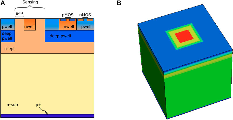
FIGURE 1. (A) Schematic of the ARCADIA pixel. (B) TCAD 3D single-pixel simulation domain. The color scale refers to the doping concentration.
The process allows for the integration of both analog and digital CMOS circuits based on 1.2 V transistors and thus a readout electronic circuit similar to the one of a previous prototype [17]. A more compact circuit, such as the one used in the ALPIDE chip [12], has also been designed and will be tested in a dedicated prototype. A more detailed description of the processing is provided in [16].
The ARCADIA collaboration is currently working on a large-area prototype of 1.3 × 1.3 cm2 active area consisting of 512 × 512 pixels with 25 μm pitch, to be realized in a first engineering run with integrated digital electronics. Additional test structures of pixel matrices with pixel pitches ranging from 10 to 50 μm and total thicknesses of 50–300 μm will also be produced. In the following, we report on the simulations and the optimization procedures of the sensor designs that have been developed in preparation of the production run.
This study is organized as follows: Section 2 describes the pixel geometry and the simulation settings that were used in the analysis of the device characteristics. Additionally, the radiation damage models used for the predictions after irradiation are introduced, and the first observations are discussed. The optimization targets, methods, and results are described in Section 3. The conclusions are given in Section 4.
2 TCAD Simulations
The electrical characteristics of the pixels are analyzed using Technology Computer Aided Design (TCAD) simulations1. The TCAD simulation domains are realized in 3D, as visualized for a single-pixel domain with 50 μm thickness, in Figure 1B. The collection electrode is biased at + 0.8 V, and the reverse bias voltage is applied from the back side of the pixel. Three different substrate thicknesses of 50, 100, and 300 μm are simulated, using the same doping profiles provided by the foundry. This basic simulation setup has been previously validated with a production series, under the SEED project [17].
All simulations, if not stated otherwise in the figures, are performed at 300 K.
The simulations neglect the nwell regions used in the implementation of PMOS transistors, assuming that the electrical characteristic and the radiation detection are not significantly affected.
Due to the wide range of planned applications, these studies include a detailed analysis of the impact of different radiation levels on the pixel characteristics using radiation damage models for both the silicon bulk and the Si-SiO2 interface. The adopted models, as well as the simulation results, are discussed in Section 2.2.
2.1 Electrical Characterization
An example of the capacitance-voltage (CV) and current-voltage (IV) curves of a 50 × 50 μm2 pixel is shown in Figure 2B. The CV characteristics are, if not stated differently, simulated in AC with a frequency of 10 kHz. The black curve in Figure 2B represents the current measured at the collection diode and has been obtained from two half-pixel domains, shown in Figure 2A, with a 10 mV voltage difference applied at the top electrodes. In this way, a non-negligible current is flowing between the pixels if the substrate is not fully depleted. The red and blue curves correspond to the current measured at the top pwell and capacitance measured at the collection electrode in single-pixel simulations, respectively. The dotted and dashed lines highlight the depletion voltage and onset of the punch-through currents, respectively. Both IV curves feature the point of sign change from negative to positive current values in the form of dips in their absolute spectrum. These are defined as the voltage needed for full depletion Vdpl and onset of the punch-through currents Vpt and correspond to the moment in which the single pixels become isolated from each other through the depletion region and the moment in which the exponential increase of hole current between the pwell implantations and the backside p+ contact starts. The sensors can be biased at a voltage higher than Vpt as long as the power consumption is not too large. Therefore, it is useful to extract the maximum allowed bias voltage at which a power consumption of 0.1 mW/cm2 is reached. This voltage is marked as a dotted red line and will be referred to as Vpw in the following.
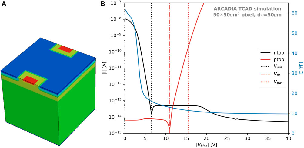
FIGURE 2. (A) Example of a 3D TCAD simulation domain of two half-pixels. The color scale refers to the doping concentration. (B) Simulated IV and CV curves of the standard 50 × 50 μm2 pixel in dSi = 50 μm thickness. The black curve shows the absolute current measured at the collection electrode, and the red curve corresponds to the current measured at the pwell on the top side of the sensor. The blue curve shows the capacitance of the full structure over the applied bias voltage range. The dotted black, dashed red, and dotted red lines mark the voltages of depletion Vdpl, the onset of the punch-through current Vpt, and reached maximum power consumption Vpw, respectively.
As it is visible in Figure 2B, comparing the black dotted line and blue curve, the depletion voltage of these devices does not necessarily correspond to the voltage at which the minimum capacitance is reached. Due to the low-doped epitaxial layer, full depletion of the substrate including the epi-layer is only achieved at much higher voltages.
In the following analysis, capacitances and leakage currents are extracted at Vpt, which have been chosen as an optimal and safe operating point.
2.2 Prediction of Radiation Tolerance
The ARCADIA sensors are designed for a wide range of applications, which include HEP collider experiments. Future collider experiments, like the FCC, require good timing performance and (partially) high-radiation tolerance, especially for the central tracking and vertex detectors [18, 19].
Ionizing radiation not only damages the surface of the sensor, which produces oxide charges at the interface between the Si and SiO2 surface, but also creates cluster and point-like defects in the silicon crystal lattice. These defects result in new energy levels within the bandgap and can function as traps, which get electrically active when occupied, thus changing the electrical properties of the sensors, such as the depletion voltage (effective doping concentration) and the leakage (or dark) current.
For a most realistic prediction of the impact of these defects, we have modeled both damage types, following the so-called new Perugia model [20, 21]. This three-trap model introduces two acceptors and one donor state in the bandgap for the description of non-ionizing radiation damage in the silicon bulk. In addition, two trap states at the Si-SiO2 interface are introduced to describe the effects of ionizing energy losses, together with fixed oxide charges which build up due to trapped charges in the SiO2 layer.
While this model has been tuned and validated on p-type silicon, it has shown good performance for sensors produced by different vendors [20]. These results make us confident that the model has a good qualitative predictive power also for the ARCADIA sensors. However, a variation in absolute values of leakage current and capacitance can be expected due to varying impurity concentrations in the substrate.
2.2.1 Surface Damage
To estimate the impact of surface damage on the sensor properties, we have employed a SiO2 layer that features positive oxide charges. The concentration of these charges increases with the modeled total ionizing dose (TID), along with defect levels in the bandgap. We are following the model introduced and summarized in [21]. The trap and oxide charge concentrations are plotted as a function of the 1 MeV neutron equivalent fluences and the dose in Figure 3. Here, the fluence dose relation is used for 24 GeV protons of the CERN Proton Synchrotron with a proton hardness factor of 0.6 and a damage factor of D/ϕ = 3.3 × 10⁻⁸rad/(proton/cm2) [22]. Because most potential applications of the ARCADIA technology do not expect doses greater than 10 krad, this value has been chosen as a reference for capacitance and leakage current estimates. This study, however, includes predictions for doses of up to 1 Grad, due to the availability of models describing radiation damage induced by high doses and in view of a validation of this technology for harsh environments.
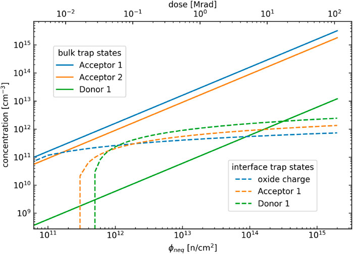
FIGURE 3. Trap concentrations as a function of the neutron equivalent fluence (bottom axis) and total ionizing dose (top axis) [21]. The solid and dashed lines correspond to the trap states in the silicon bulk and at the Si‐SiO2 interface, respectively. The trap properties are listed in Table 1.
The impact of the SiO2 and of the induced positive oxide charges is visible in the CV curves, as presented in Figure 4A, of the example of a 50 × 50 μm2 pixel. An increase of the capacitance is observed over the full voltage range (from 0 to −50 V). This effect is present for all the pixel pitches. The CV curve without the SiO2 layer is represented by the black line and shows the smallest values. When the SiO2 layer is included, with a minimal concentration of positive oxide charge and traps, an increase of about 3 fF at the depletion voltage (−6.5 V) is observed. The capacitance more than doubles with an increasing dose of up to 5 Grad (50 MGy), the capacitance more than doubles. The first increase of the capacitance at the depletion voltage Cend(Vdpl) for low doses (
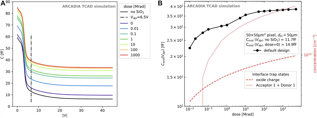
FIGURE 4. (A) Capacitance‐voltage characteristics of a 50 × 50 μm2 pixel in dSi = 50 μm thickness, for different total ionizing doses. The dashed line corresponds to the depletion voltage of Vdpl = 6.5 V. (B) The capacitance at the depletion voltage Vdpl of the 50 × 50 μm2 pixel as a function of the total ionizing dose. The red dashed and dotted lines correspond to the concentration of positive oxide charges and the sum of the two trap concentrations at the Si‐SiO2 interface, respectively.
The main impact of the increased trap concentration is a higher surface recombination velocity, while the positive oxide charges attract free electrons from the n-type epi layer and create an effective extension of the collection electrode. This effect is schematically visualized in the top plot of Figure 5A, and its impact on the electrostatic potential and the electric field lines is shown in Figure 5B.
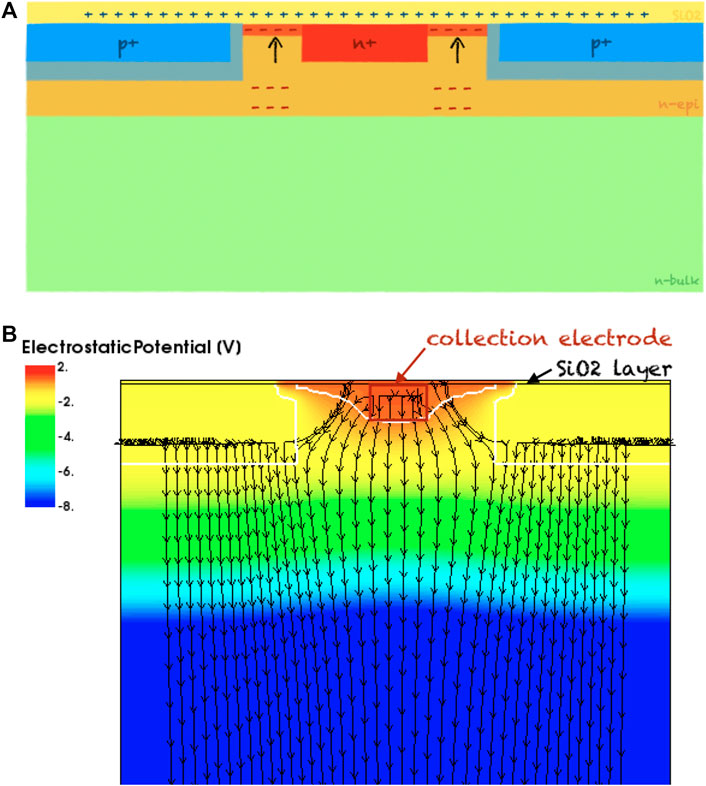
FIGURE 5. (A) Schematic of the impact of positive oxide charges at the interface between silicon and Si-SiO2. (B) Electrostatic potential across the center of a 25 × 25 μm2 pixel including a SiO2 layer and positive oxide charges corresponding to 50 Mrad total ionizing dose. The black arrows show the electric field lines, and the white lines mark the depletion region.
The strength of this effect depends on the sizes of the collection electrode and of the implant-free gap size between the diode and the pwell of the pixel. This allows for an optimization of the geometry and will be further discussed in Section 3.1.
2.2.2 Bulk Damage
To simulate the pixels’ electrical characteristics after irradiation with hadrons, we have employed three trap models, similar to [23, 24]. The main properties, like the activation energy, and the capture/emission cross-sections for electrons and holes of the defect levels are summarized in Table 1.
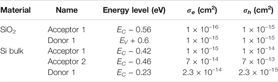
TABLE 1. Properties for the two surface and three bulk traps [21]; listed as in which material they are introduced, how they are named in Figure 3, which energy level in the Si bandgap they occupy, and their electron σe and hole σh capture cross-sections, respectively.
The concentration of these traps increases linearly with the fluence, as shown in Figure 3, and this results in a linear increase of the leakage current. This effect is shown in Figure 6, together with the comparison of a simple scaling of the current from low (T1 = 248 K) to high (T2 = 300 K) temperatures, following [25]:
with Eg,eff = 1.214 eV. Figure 6 shows the measured leakage current at Vpt as a function of the fluence ϕneq for 50 × 50 μm2 pixels in 50 μm thickness. The first observation is that the induced surface damage has no significant impact on the leakage current, which is dominated by the volume generation currents induced by the bulk defects.
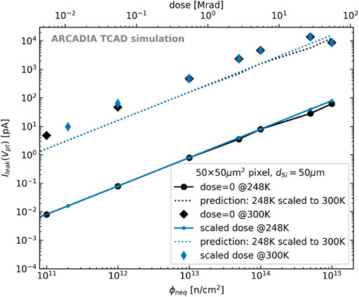
FIGURE 6. Leakage current of a 50 × 50 μm2 pixel in dSi = 50 μm thickness as a function of the fluence. The black markers and lines correspond to a fixed dose of zero, while the blue markers/lines show the results for increasing concentrations of traps and oxide charges at the Si‐SiO2 interface. The circular markers correspond to simulations run at 248 K, and the diamonds show the results at 300 K.
The second observation is made using Eq. 1 to scale the values measured at 248 K up to room temperature (shown in dotted lines). Since the model parameters are fitted to measurements at 248 K, it has to be mentioned that we observe a difference between the simulation results at 300 K and the scaling from 248 K, of factor three.
Evaluating the operating voltages as a function of the fluence (Figure 7), a drop in the depletion voltage is visible for fluences
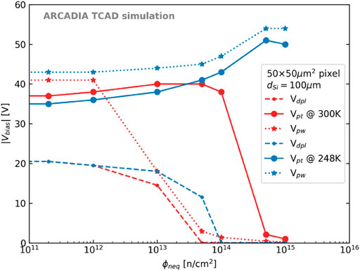
FIGURE 7. Operating voltage of 50 × 50 μm2 pixel in dSi = 100 μm thickness as a function of the fluence. The blue curves refer to simulations run at a temperature of 248 K, while the red curves refer to a temperature of 300 K.
In conventional Si diodes, the depletion voltage is expected to increase after the inversion of the effective doping of the silicon bulk [26]. However, for these pixel sensors, the depletion voltage is defined as the reverse voltage at which neighboring pixels become isolated by a depletion region, which corresponds to full bulk depletion before irradiation. But as soon as the bulk is type-inverted, the depletion region starts to grow from the front side between the epi layer and the bulk; therefore, already with the small applied voltage of 0.8 V at the collection electrode, the electrodes of the pixels become isolated without any reverse bias applied.
The type-inversion of the sensors above fluences of 1 × 1014 cm−2 can be confirmed by comparing transient simulations of minimum ionizing particles (MIPs) using the HeavyIonModel of TCAD [27]. This model was used to simulate the charge deposition along a track within the sensor, defining the amount of generated charge as a function of the path length by the linear energy transfer (LET). Complementary Geant4 simulations have been used to confirm the average charge deposition of MIPs of ∼ 80 e/h pairs or 1.28 × 10⁻⁵ pC per μm. The charge deposition is instantaneously introduced after 10 ps, and the resulting transient signal is shown in the top plot of Figure 8A for a MIP incident in the pixel center, along a perfectly perpendicular trajectory, for fluences from zero up to 1 × 1015 cm−2. The transients have been simulated at Vbias = −30 V, thus well above the depletion voltage over the full fluence range, and the time necessary to reach 95 and 99% charge collection efficiency (t95 and t99), respectively, is reported in the plot on the bottom. In order to avoid inaccuracies of the simulation that impact the results, these times are defined as:
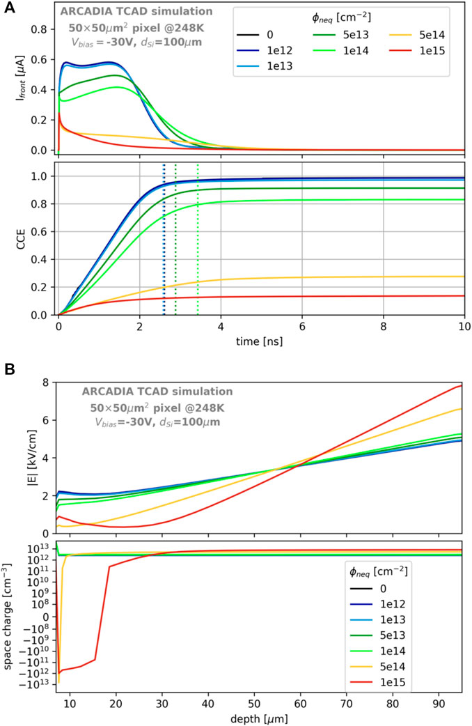
FIGURE 8. (A) Current signals (top) and charge collection efficiency (bottom) of a 50 × 50 μm2 pixel in dSi = 100 μm thickness, after neutron equivalent fluences of 0–1 × 1015 cm−2, simulated at Vbias = − 30 V. The dotted lines mark the time of 95% charge collection. (B) Electric field (top) and space charge (bottom) as a function of the sensor depth for different fluences in the same pixel sensor.
At low fluences
The occupation of traps is dependent on the amount of available free charge carriers, as well as on the leakage current, the applied bias voltage, and the capture cross-sections. This results, e.g., in a stronger double junction at higher temperatures due to easier occupation of the traps and higher leakage currents. Since the employed trap model has been fit to data at 248 K [21], we report here only the results at 248 K. It should be mentioned that the amount and the type of radiation-induced bulk defects depend on the particle type as well as on the particle energy of the irradiation [29]. In addition, the original impurities within the Si, like oxygen, can support or prevent the creation of certain defects [30, 31].
3 Design Optimizations
The pixel design optimization targets a small pixel capacitance to ensure low electronics noise, thus maximum signal to noise ratio, and high charge collection efficiencies within the smallest possible time windows in order to decrease dead-times for high particle rates.
To choose only a few geometries for each pixel pitch (10 μm, 25 μm, and 50 μm) with optimal performance, a large range of simulations with the different electrode and pwell sizes has been performed. The results of this simulation campaign are summarized into three different categories, focusing 1) on the pixel capacitance (Section 3.1), 2) on the bias voltage operating range (Section 2.1), and 3) on the charge collection (Section 3.3).
3.1 Minimizing the Pixel Capacitance
The pixel capacitance can be lowered by decreasing the size of the collection electrode. However, due to the impact of the positive oxide charges within the gap between the electrode and the pwell, the gap size plays a major role, and both quantities have to be analyzed in parallel. In the following, bulk damage is not considered in the comparisons between pixel designs, due to a negligible impact on the pixels’ capacitance. An example of the importance of the gap size is visible in Figure 9A. The capacitance is shown as a function of the dose for small, medium, and large electrode sizes with default and optimized gap sizes. Here, the dose range has been limited to (0–100) krad, which covers the expected doses reached after a few years of operation within a medical scanner used for proton CT. Comparing the small electrode with the default gap size shows, without the recognition of the SiO2 layer and without positive oxide charges, a smaller capacitance than the medium electrode with optimized gap size. However, as soon as oxide charges are introduced, the trend turns around, and the capacitance of the medium electrode stays ∼30% lower than the capacitance of the non-optimized small electrode. While Figure 9A only shows the results for the 50 μm thick sensor, the same effect and very comparable absolute values have been found for thicker substrates.
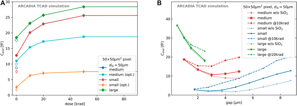
FIGURE 9. (A) Capacitance of 50 × 50 μm2 pixels in dSi = 50 μm thickness, as a function of the total ionizing dose for five different pixel sensor layouts. The dots, diamonds, and triangles correspond to the results obtained for a medium, small, and large collection electrode size, respectively. The light blue dots and orange diamonds show the results after the optimization of the gap size between the pwell and the electrode for minimal capacitance. The open markers correspond to the simulation results without the SiO2 layer. (B) The capacitance of 50 × 50 μm2 pixels in dSi = 50 μm thickness, with small, medium, and large collection electrode size as a function of the gap size between the pwell and the electrode.
The capacitance for three different electrode sizes is shown as a function of the gap size for 50 × 50 μm2 pixels in Figure 9B. Due to boundary conditions, the pwell has a minimum size to facilitate the integration of transistors for the electronics; hence, the gap size range is limited and most restricted for the largest electrode. For the 50 × 50 μm2 pixel, we find a minimum capacitance for all electrode sizes at ∼ 2.5 μm gap size, for simulations that include the SiO2 layer. In the case of the large electrode size, it can be clearly seen that the capacitance decreases with increasing gap size, which corresponds to a smaller pwell size.
3.2 Operating Bias Voltage
The pixel designs for the different pitches impact these parameters due to changes in the electrostatic potential. Since the pixel design for the 25 μm pitch of the ARCADIA main demonstrator chip is fixed, its operating parameters are used as a reference to allow the operation of different pixel flavors on the test-structure.
Figure 10 shows the bias voltages (Vdpl, Vpt, and Vpw) for the three different thicknesses of the 10 × 10 μm2 pixels (a) and 50 × 50 μm2 pixels (b). The red shaded area marks the Vpt ± 10% of the reference 25 × 25 μm2 pixels. While the reference voltage lies nicely within the limits of all 50 × 50 μm2 pixel designs, the minimum bias voltage of the 10 × 10 μm2 pixels varies strongly for the different designs. Only one design, with a large pwell, can be considered operational (depleted) at the reference voltage.
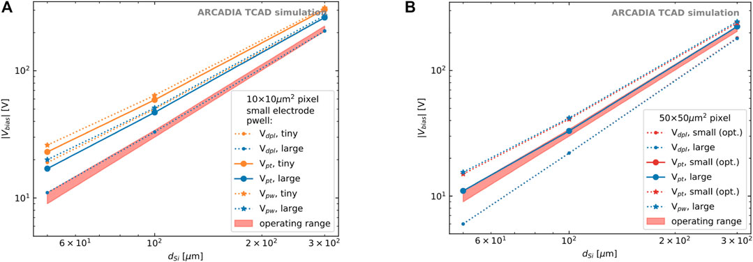
FIGURE 10. Bias voltage at depletion Vdpl (small dots), at the onset of the punch-through currents Vpt (large dots), and at the point of maximum power consumption Vpw (stars), for 10 × 10 μm2 pixels (A) and 50 × 50 μm2 pixels (B). The red shaded area corresponds to the Vpt ± 10% of the reference 25 × 25 μm2 pixel.
The large difference in the operating bias voltage for the 10 × 10 μm2 pixels has been an important observation and led to the conclusion that the test-structures with these pitches will be separated from the others in the final layout. This will ensure that a sufficient bias voltage can be applied from the front and back sides of the sensors for thicknesses of 50 μm and 100/300 μm, respectively.
3.3 Uniform Response
Transient simulations of MIP-like tracks have been used to evaluate the charge collection and response across the pixels. To evaluate the signals, usually the best- and worst-case scenarios are studied, which correspond to a traversing particle at the center and the corner of the pixel. For the comparison of different pixel designs, the time to collect 95 and 99% of the generated charges has been used. While charge losses due to radiation damage in the silicon crystal are not expected to vary between the pixel designs but rather with the substrate thickness, the study of response uniformity is neglecting bulk damage. The impact of surface damage on the signal formation has been tested in transient simulations and has been found to be negligible.
A general observation of the necessary time to collect 99% of all charges in the pixel corner is the strong dependence on the pwell width (Figure 11). Additionally, a large collection electrode size improves the collection of the charges from the corners of the pixels. However, the electric field strength below the collection electrode decreases with an increased collection node, which results in a slightly slower collection in the pixel center. Considering a homogeneous distribution of particles across the full area of the chip, this motivates an optimization for uniformity rather than peak performance in localized areas.
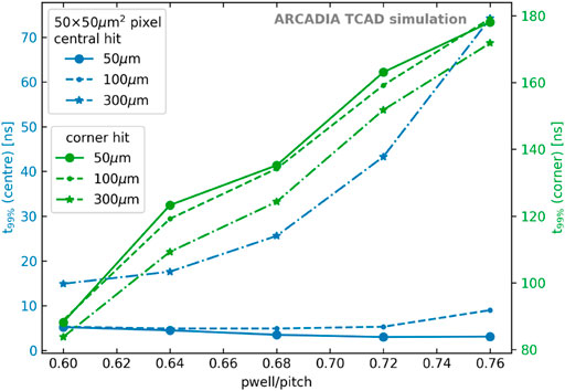
FIGURE 11. Time required for 99% charge collection in the center (blue) and corner (green) of 50 × 50 μm2 pixels with medium-sized nwell, as a function of the pwell over pitch ratio. The results are shown for three different sensors thicknesses.
These considerations lead to a choice of 25 × 25 μm2 and 50 × 50 μm2 pixels, with minimum pwell and maximal electrode size. Due to the small pitch, the 10 × 10 μm2 pixels are much less affected by slow charge collections in the pixels’ corners. Instead, charge sharing is much more pronounced, and the larger concern lies in the so-called channel choking, which describes the effect of a potential barrier occurring when the sensing window becomes too small in comparison to the pwell size. To overcome this problem, a design that features the electronics in islands of deep pwells within the pixel corners has been studied, and a picture of a 2 × 2 pixel matrix is shown in Figure 12A. With this approach, a large enough (deep) pwell size can be achieved to allow for the integration of the electronics without the risk of a non-functional diode.
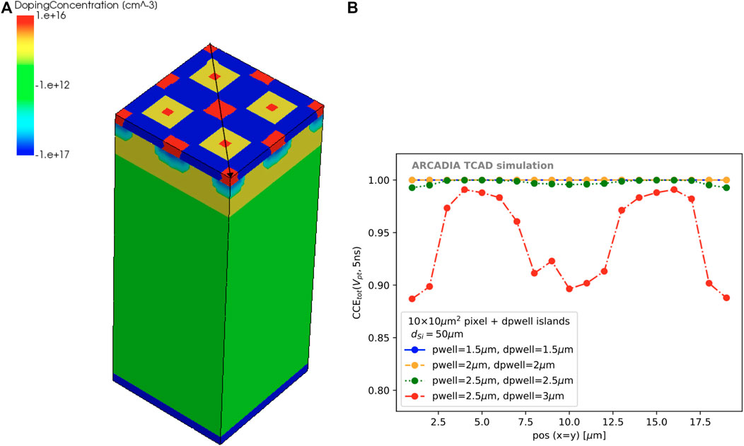
FIGURE 12. (A) 2 × 2 pixel matrix of 10 × 10 μm2 pixels with deep pwell islands in the pixel corners. The black arrow indicates the direction of the position scan. (B) Charge collection efficiency after 5 ns for 10 × 10 μm2 pixels with deep pwell islands and dSi = 50 μm, presented as a function of the position along the diagonal indicated in (A). The differently colored curves correspond to different (d) pwell sizes, which values are given in the legend.
The resulting charge collection efficiencies for a range of (deep) pwell sizes, given here in half-sizes, are presented in Figure 12B at t = 5 ns for particles incident along the diagonal of the 2 × 2 pixel matrix. The first observation is that for deep pwell size
4 Conclusion
The first engineering run of the ARCADIA main demonstrator is currently in production. The preparations have been accompanied by a large simulation campaign to study possible improvements of the pixel designs in order to decrease the pixel capacitance and optimize the charge collection. This campaign included first tests of radiation tolerance, using the latest radiation damage models, and has investigated in detail the impact of surface charges on the electrical properties. The capacitance of the selected designs is summarized in Figure 13A and is shown before and after a dose of 10 krad is applied. Without surface damage, all pixels feature a single-pixel capacitance
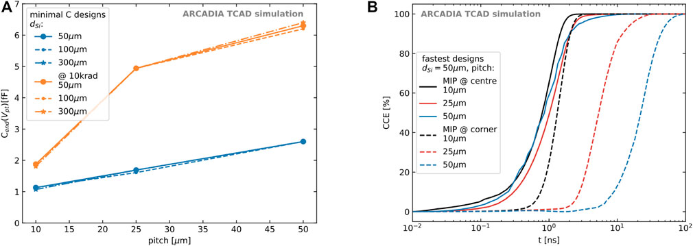
FIGURE 13. (A) Capacitance at Vpt for the optimized designs of pixels with 10, 25, and 50 μm pitch, at a dose equal to 0 in blue and after a dose of 10 krad in orange. (B) Charge collection efficiencies for MIPs impinging at the center (straight lines) and corner (dashed lines) of the pixels, for the selected design of pixels with 10, 25, and 50 μm pitch, before irradiation.
The charge collection efficiencies for the fastest designs are shown in Figure 13B, for central (straight) and corner (dashed) hits. The times for 99% CC are summarized in Table 2.
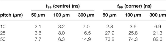
TABLE 2. Times for 99% charge collection for MIP-like charge depositions at the center and the corner for pixels with three different pitches, given for three substrate thicknesses (50/100/300) μm.
These studies led to the choice of a few different designs of pixels with 10/25/50 μm pitch that will be realized in a number of test-structures, such as matrices of 1 × 1 and 2 × 2 mm2. These structures will allow a validation of the physics models used in the simulation and will be characterized using, besides basic IV and CV measurements, radioactive sources and a laser for e/h pair generation.
Data Availability Statement
The raw data supporting the conclusion of this article will be made available by the authors, without undue reservation.
Author Contributions
TC contributed with TCAD simulations. LD contributed to the development of the software to analyze the simulation data. G-FB contributed to discussions and help in the implementation of the radiation damage models in TCAD. LP contributed with computing resources, discussions, and simulations. All authors reviewed the text of the paper. The manustript was written by CN.
Funding
The research activity presented in this article has been carried out in the framework of the ARCADIA experiment funded by the Istituto Nazionale di Fisica Nucleare (INFN), CSN5.
Conflict of Interest
The authors declare that the research was conducted in the absence of any commercial or financial relationships that could be construed as a potential conflict of interest.
Publisher’s Note
All claims expressed in this article are solely those of the authors and do not necessarily represent those of their affiliated organizations, or those of the publisher, the editors and the reviewers. Any product that may be evaluated in this article, or claim that may be made by its manufacturer, is not guaranteed or endorsed by the publisher.
Footnotes
1Synopsys Sentaurus Version P-2019.03-SP1.
References
1. Wermes N. Pixel Detectors for Charged Particles. Nucl Instr Methods Phys Res Section A: Acc Spectrometers, Detectors Associated Equipment (2009) 604(1):370–9. PSD8. doi:10.1016/j.nima.2009.01.098
2. Kemmer J, Lutz G. New Detector Concepts. Nucl Instr Methods Phys Res Section A: Acc Spectrometers, Detectors Associated Equipment (1987) 253(3):365–77. doi:10.1016/0168-9002(87)90518-3
3. Velthuis JJ, Kohrs R, Mathes M, Raspereza A, Reuen L, Andricek L, et al. Depfet, a Monolithic Active Pixel Sensor for the Ilc. Nucl Instr Methods Phys Res Section A: Acc Spectrometers, Detectors Associated Equipment (2007) 579(2):685–9. doi:10.1016/j.nima.2007.05.278
4. Niemiec H, Bulgheroni A, Caccia M, Grabiec P, Grodner M, Jastrzab M, et al. Monolithic Active Pixel Sensor Realized in SOI Technology-Concept and Verification. Microelectronics Reliability (2005) 45(7):1202–7. doi:10.1016/j.microrel.2004.10.014
5. Turchetta R, Berst JD, Casadei B, Claus G, Colledani C, Dulinski W, et al. A Monolithic Active Pixel Sensor for Charged Particle Tracking and Imaging Using Standard Vlsi Cmos Technology. Nucl Instr Methods Phys Res Section A: Acc Spectrometers, Detectors Associated Equipment (2001) 458(3):677–89. doi:10.1016/S0168-9002(00)00893-7
6. Turchetta R, French M, Manolopoulos S, Tyndel M, Allport P, Bates R, et al. Monolithic Active Pixel Sensors (Maps) in a Vlsi Cmos Technology. Nucl Instr Methods Phys Res Section A: Acc Spectrometers, Detectors Associated Equipment (2003) 501(1):251–9. doi:10.1016/S0168-9002(02)02043-0
7. Marinas C. The Belle II Pixel Detector: High Precision with Low Material. Nucl Instr Methods Phys Res Section A: Acc Spectrometers, Detectors Associated EquipmentPIXEL (2013) 731:31–5. doi:10.1016/j.nima.2013.03.025
8. Lutz G, Aschauer S, Majewski P, Holl P, Strüder L. The DEPFET Detector-Amplifier Structure for Spectroscopic Imaging in Astronomy and for Experiments at Free Electron Lasers. Nucl Instr Methods Phys Res Section A: Acc Spectrometers, Detectors Associated Equipment (2017) 845:122–7. doi:10.1016/j.nima.2016.04.049
9. Lan H, Wang Y, Chen J, Cao F, Hu H-F. A Review of SOI Monolithic Active Pixel Sensors for Radiation Detection Applications. IEEE Sensors J (2015) 15(5):1. doi:10.1109/JSEN.2015.2389271
10. Hagino K, Yarita K, Negishi K, Oono K, Hayashida M, Kitajima M, et al. Radiation Damage Effects on Double-SOI Pixel Sensors for X-ray Astronomy. Nucl Instr Methods Phys Res Section A: Acc Spectrometers, Detectors Associated Equipment (2020) 978:164435. doi:10.1016/j.nima.2020.164435
11. Snoeys W, Aglieri Rinella G, Hillemanns H, Kugathasan T, Mager M, Musa L, et al. A Process Modification for CMOS Monolithic Active Pixel Sensors for Enhanced Depletion, Timing Performance and Radiation Tolerance. Nucl Instr Methods Phys Res Section A: Acc Spectrometers, Detectors Associated Equipment (2017) 871:90–6. doi:10.1016/j.nima.2017.07.046
12. Mager M. ALPIDE, the Monolithic Active Pixel Sensor for the ALICE ITS Upgrade, Nucl Instr Methods Phys Res Section A: Acc Spectrometers, Detectors Associated Equipment (2016) 824:434–8. doi:10.1016/j.nima.2015.09.057
13. Perić I. A Novel Monolithic Pixelated Particle Detector Implemented in High-Voltage CMOS Technology. Nucl Instr Methods Phys Res Section A: Acc Spectrometers, Detectors Associated Equipment (2007) 582(3):876–85. doi:10.1016/j.nima.2007.07.115
14. Havránek M, Hemperek T, Krüger H, Fu Y, Germic L, Kishishita T, et al. DMAPS: a Fully Depleted Monolithic Active Pixel Sensor-Analog Performance Characterization. J Inst (2015) 10(02):P02013. doi:10.1088/1748-0221/10/02/p02013
15. Giubilato P, Bisello D, Chalmet P, Denes P, Kloukinas K, Mattiazzo S, et al. LePix-A High Resistivity, Fully Depleted Monolithic Pixel Detector. Nucl Instr Methods Phys Res Section A: Acc Spectrometers, Detectors Associated Equipment (2013) 732:91–4. doi:10.1016/j.nima.2013.05.189
16. Pancheri L, Giampaolo RA, Salvo AD, Mattiazzo S, Corradino T, Giubilato P, et al. Fully Depleted MAPS in 110-nm CMOS Process with 100-300-μm Active Substrate. IEEE Trans Electron Devices (2020) 67(6):2393–9. doi:10.1109/TED.2020.2985639
17. Pancheri L, Olave J, Panati S, Rivetti A, Cossio F, Rolo M, et al. A 110 Nm CMOS Process for Fully-Depleted Pixel Sensors. J Inst (2019) 14(06):C06016. doi:10.1088/1748-0221/14/06/C06016
18.FCC Collaboration. Fcc-ee: The Lepton Collider. Eur Phys J Spec Top (2019) 228(2):261–623. doi:10.1140/epjst/e2019-900045-4
19.FCC Collaboration. Fcc-hh: The Hadron Collider. Eur Phys J Spec Top (2019) 228(4):755–1107. doi:10.1140/epjst/e2019-900087-0
20. Morozzi A, Moscatelli F, Passeri D, Bilei GM. TCAD Advanced Radiation Damage Modeling in Silicon Detectors. PoS (2020) Vertex2019:050. doi:10.22323/1.373.0050
21. Passeri D, Morozzi A. TCAD Radiation Damage modelAIDA-2020-D7.4 (2019) Available at: http://cds.cern.ch/record/2705944 Accessed November 3, 2021.
22. Mandic I, Cindro V, Kramberger G, Kristof ES, Mikuz M, Vrtacnik D, et al. Bulk Damage in DMILL Npn Bipolar Transistors Caused by thermal Neutrons versus Protons and Fast Neutrons. IEEE Trans Nucl Sci (2004) 51(4):1752–8. doi:10.1109/TNS.2004.832927
23. Folkestad Å, Akiba K, van Beuzekom M, Buchanan E, Collins P, Dall’Occo E, et al. Development of a Silicon Bulk Radiation Damage Model for Sentaurus Tcad. Nucl Instr Methods Phys Res Section A: Acc Spectrometers, Detectors Associated Equipment (2017) 874:94–102. doi:10.1016/j.nima.2017.08.042
24. Moscatelli F, Passeri D, Morozzi A, Mendicino R, Dalla Betta G-F, Bilei GM. Combined Bulk and Surface Radiation Damage Effects at Very High Fluences in Silicon Detectors: Measurements and TCAD Simulations. IEEE Trans Nucl Sci (2016) 63(5):2716–23. doi:10.1109/TNS.2016.2599560
25. Sze S, Ng KK. Physics of Semiconductor Devices. Hoboken, New Jersey: Wiley-Interscience (1995). p. 739–51.
26. Wunstorf R. Systematische Untersuchungen zur Strahlenresistenz von Silizium-Detektoren für die Verwendung in Hochenergiephysik-Experimenten. PhD thesis. Hamburg, Germany: Hamburg University (1992). Available at: https://bib-pubdb1.desy.de/record/153817 Accessed November 3, 2021.
27.Synopsys. Sentaurus Device User Guide. Version P-2019.03 (2019). Avilable at: https://www.synopsys.com/silicon/tcad/device-simulation/sentaurus-device.html Accessed November 3, 2021.
28. Chiochia V, Swartz M, Allkofer Y, Bortoletto D, Cremaldi L, Cucciarelli S, et al. A Double junction Model of Irradiated Silicon Pixel Sensors for LHC. Nucl Instr Methods Phys Res Section A: Acc Spectrometers, Detectors Associated Equipment (2006) 568(1):51–5. doi:10.1016/j.nima.2006.05.199
29. Kuhnke M, Fretwurst E, Lindstroem G. Defect Generation in Crystalline Silicon Irradiated with High Energy Particles. Nucl Instr Methods Phys Res Section B: Beam Interactions Mater Atoms (2002) 186(1):144–51. doi:10.1016/S0168-583X(01)00886-2
30. Neubüser C. Impact of Irradiations by Protons with Different Energies on Silicon Sensors, Master’s thesis. Hamburg, Germany: Hamburg University (2013). Availabe at: https://cds.cern.ch/record/2636089 Accessed November 3, 2021.
Keywords: MAPS, radiation detectors, CMOS, TCAD simulations, pixel detectors
Citation: Neubüser C, Corradino T, Dalla Betta G-F, De Cilladi L and Pancheri L (2021) Sensor Design Optimization of Innovative Low-Power, Large Area FD-MAPS for HEP and Applied Science. Front. Phys. 9:625401. doi: 10.3389/fphy.2021.625401
Received: 02 November 2020; Accepted: 11 October 2021;
Published: 16 November 2021.
Edited by:
Christer Frojdh, Mid Sweden University, SwedenCopyright © 2021 Neubüser, Corradino, Dalla Betta, De Cilladi and Pancheri. This is an open-access article distributed under the terms of the Creative Commons Attribution License (CC BY). The use, distribution or reproduction in other forums is permitted, provided the original author(s) and the copyright owner(s) are credited and that the original publication in this journal is cited, in accordance with accepted academic practice. No use, distribution or reproduction is permitted which does not comply with these terms.
*Correspondence: Coralie Neubüser, Y29yYWxpZS5uZXVidWVzZXJAdGlmcGEuaW5mbi5pdA==