 Jia-Xin Zhang1,2,3
 Wei Wang1,2,3Zai-Bo Li1,3Hai-Feng Ye1,3Run-Yu Huang1,3Ze-Peng Hou1,3Hui Zeng1,3Hong-xia Zhu1,3Chen Liu1,3Xue-Yan Yang1,3
 Yan-Li Shi1,3*
- 1School of Physics and Astronomy, Yunnan University, Kunming, China
- 2Shanxi Guohui Optoelectronic Technology Co Ltd., Taiyuan, China
- 3Key Laboratory of Quantum Information of Yunnan Province, Yunnan University, Kunming, China
A 1280 × 1,024 In0.53Ga0.47As short wave infrared (SWIR) focal plane array (FPA) detector with a planar-type back-illuminated process has been fabricated. With indium bump flip-chip bonding techniques, the InGaAs photodiode arrays were hybrid-integrated to the CMOS readout integrated circuit (ROIC) with correlated double sampling (CDS). The response spectrum is 0.9–1.7 μm. The test results show that the dark current density is 2.25 nA/cm2 at 25 °C, the detectivity D* is up to 1.1 × 1013 cm · Hz1/2/W, the noise electron is as low as 48 e− under correlated double sampling mode, the quantum efficiency is 88% at 1550 nm, and the operability is more than 99.9%. Moreover, the dark current and noise electron have been studied theoretically in depth. The results indicate that the diffusion current is the main contribution of the dark current, and the readout integrated circuit noise electron is the main source of FPA noise.
Introduction
PIN InGaAs shor twave infrared (SWIR) focal plane array (FPA) detectors have attracted extensive attention due to their high detectivity [1], high quantum efficiency, room temperature operation, low dark current, and good radiation resistance [2]. Furthermore, InGaAs FPA detectors have wide applications in many fields, such as aviation safety [3], biomedicine [4], camouflage recognition [5], and infrared night vision [6]. Recently, InGaAs SWIR FPAa detectors are being developed to reduce the pitch and enlarge the format [7,8]. Aerius Photonics reported a 1,280 × 1,024 20 μm InGaAs FPA detector. The dark current density was 3.85A/cm−2 at 25°C, and the operability was 99.88% [9]. SCD developed a 1,280 × 1,024 InGaAs FPA detector with a pitch of 10 μm. The quantum efficiency (QE) at 1550 nm was 80%. The dark current density was 0.5 nA/cm2at 7°C, and the operability was 99.5% [10]. FLIR researched and developed a 1,280 × 1,024 15 μm InGaAs detector. The QE was up to 70%. The noise electron was as low as 70 e− in middle gain at 20°C, and the operability was up to 99.5% [11]. For space application, it is critical to develop large-format PIN arrays with low pitch and low dark current density at higher operation temperatures. However, dark current densities reported up to now have been more than 3 nA/cm−2 at room temperature, and lower dark current density is required to gain higher sensitivity which is very important for low light level applications.
The lattice matching of In0.53Ga0.47As with an InP substrate constitutes a significant advantage that limits defect density and reduces Shockley Read Hall generation-recombination dark currents. The high crystalline quality material is the key point to reduce the dark current. Zn diffusion depth is another process that affects dark current. If Zn diffusion depth exceeds the InP/InGaAs hetero-interface, the InGaAs is damaged and dot defects are caused by Zn impurity. The dot defects become carrier recombination centers in the InGaAs absorption layer precisely [12,13]. In this paper, the fabrication of a high performance 1,280 × 1,024 InGaAs SWIR FPA detector with a pitch of 15 μm is presented. The device was processed with a planar-type back-illuminated process by flip-chip bonding with indium bump. The EPI material quality was optimized and the Zn diffusion depth was controlled precisely to reduce dark current. The test results show that the dark current density is 2.25 nA/cm2 at 25°C, the operability is up to 99.98%, and the QE is 88% at 1550 nm. Moreover, the contributions of various dark current and noise electronic mechanisms are analyzed theoretically.
Fabrication of InGaAs SWIR FPA
EPI Structure Growth
The typical PIN InGaAs/InP heterostructure was grown by metal-organic chemical vapor deposition on 4-inch n+ type InP substrates. The EPI structure consisted of a 0.4 μm n+-InP buffer layer, a 2.8 μm In0.53Ga0.47As absorption layer, and a 1 μm n-InP cap layer. The defect density of the EPI was 0.1 /cm2.
InGaAs FPA Fabrication
The development and design of InGaAs FPA are common for all array formats. The active region is composed of PIN photodiodes and surrounded by common N-contact pixels to apply a uniform polarization voltage. First, a SiN layer was deposited on the EPI wafer by ICPECVD after pre-cleaning with 1%HCl, then the Zn diffusion hole was fabricated with SiN dry and wet etching, and Zn diffusion with Zn3P2 in tube. Figure 1 shows a cross-section of Zn diffusion from a scanning electron microscopic (SEM). After that, the second SiN layer was deposited on the wafer for Zn activation anneal and SiN dry-etched for p-metal evaporation. Second, the InP and InGaAs around the active region were etched to exposed n+-InP buffer layer for n-type metal evaporation with E-beams, then P-metal and N-metal were annealed for ohmic contact. Third, the connecting metal was deposited with E-beams, and then InP substrate was lapped and polished for anti-reflection coating layer deposition. Figure 2 shows an SEM cross-section of the PDAs. The fourth step is indium bump evaporation and reflow, and an SEM image of the indium bump after reflow is shown in Figure 3. During the whole process, the Zn diffusion depth was controlled to the InGaAs/InP hetero-interface precisely by optimizing the diffusion time and temperature. The contact resistance of P-metal and N-metal are 2.69 × 10⁻⁵ Ω cm2 and 2.81 × 10⁻⁷ Ω cm2, respectively. Finally, after wafer dicing, the InGaAs PDAs were hybrid-integrated to CMOS ROIC with indium bump by flip-chip bonding. The ROIC circuit adopts snapshot mode, supporting integral-then-readout and integral-while-readout modes, and CDS mode. CDS mode is used to reduce KTC noise and fixed pattern noise. Figure 4 is the schematic diagram of the ROIC circuit. Finally, the 15 μm 1,280 × 1,024 InGaAs FPA detector was packaged with high vacuum integrity metallic packaging and thermoelectric coolers. Figure 5 is the packaged FPA chip assembly. According to the above process, the smaller format 640 × 512 15 μm InGaAs SWIR detectors were fabricated and applied in space exploration in 2019.
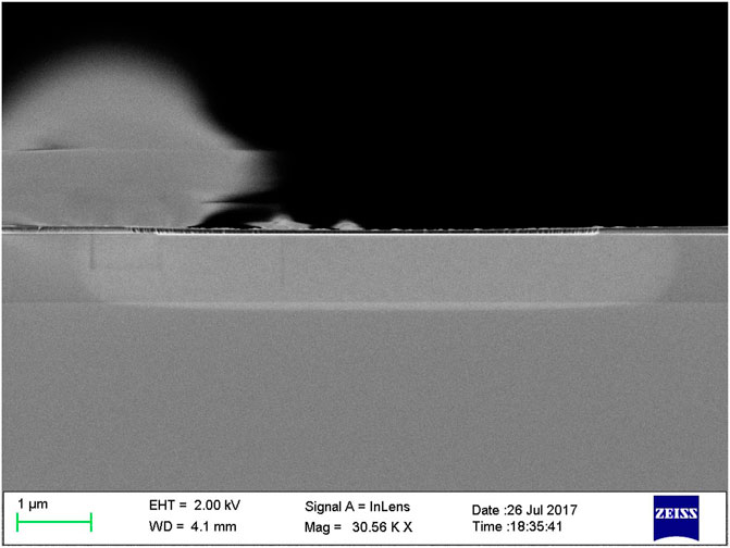
FIGURE 1. Cross-section of Zn diffusion.
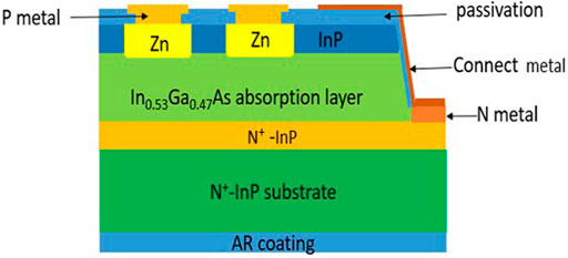
FIGURE 2. Cross-section of PDA
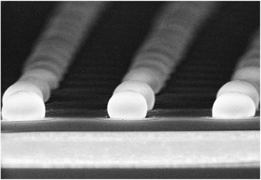
FIGURE 3. The In bump after reflow.
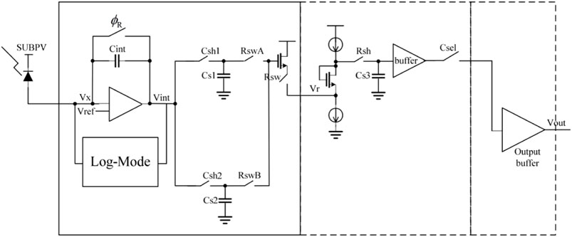
FIGURE 4. The circuit of ROIC.
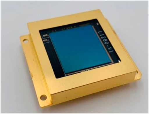
FIGURE 5. Packaged FPA chip.
Test Results
With the Pulse Instruments 7700 FPA test system and EMVA 1288 standard method, we tested the electrical characteristics and spectral response characteristics of the detector. The operability is up to 99.98%. The response non-uniformity is 4.2%. The quantum efficiency is 88% @1550 nm. The detectivity D* reaches 1.1 × 1013 cm⋅Hz1/2/W under CDS mode, and the readout noise electron is 48 e− under CDS mode. The dark current density is measured as low as 2.25 nA/cm2 and 5.06fA/pixel @ 25°C, as shown in Figure 6. The histogram of the dark current is shown in Figure 7, which is from a third party. The mean dark current of the pixels is about 10 fA/pixel at 33°C. Because of the high temperature, the result is different from our measurements, but both results indicate that the dark current is very low. The dynamic range is 64dB. The responsivity is 1.1A/W. Table 1 is the performances compared with other detectors.

FIGURE 6. The dark value versus exposure time.
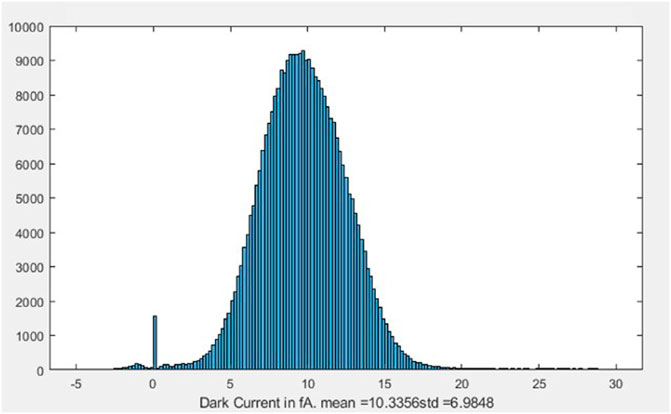
FIGURE 7. Histograms of the dark current at 33°C.

TABLE 1. Performance comparison of 1K×1KInGaAs FPA.
Performance Analyses
Dark Current
Dark current is a key parameter which must be decreased to improve signal to noise ratio and minimize the noise equivalent power. Dark current is composed of diffusion current, generate-recombination current, tunneling current, surface leakage current [13]. Dark current density Jexp is 2.25nA/cm2 at −0.1V with EMVA1288 standard method, as shown in Fig 6. At the same time, the dark current was measured on test cells for photodiode diameters varying from 6 μm to 200μm, as shown in Fig 8. Diffusion current density Jdiff, generated-recombined current density Jgr and the sum of them Jtotal are calculated with the formulae (1) and (2)[13], respectively. Intrinsic carrier concentration ni is given by formula (3) and depletion width Wd is given by formula (4)[13]. From calculation, the diffusion current density Jdiff is 1.82nA/cm2 and the generated-recombined dark current density Jgr is 0.39nA/cm2 at −0.1V. Hence, the generated-recombined dark current density Jgr is about one fifth of the diffusion dark current density. The diffusion current density Jdiff is the main contribution of the dark current density. The gap between Jtotal and Jexp comes from tunneling current density and the surface leakage current density, and becomes bigger with reverse bias increase, as shown in Fig 9. The further experimental analyses demonstrate the gap is main contributed by the tunneling current which becomes bigger with reverse bias increase.
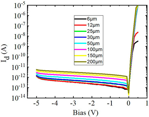
FIGURE 8. Dark current versus bias.
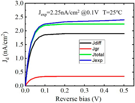
FIGURE 9. Dark current density versus reverse bias.
The dark current density can also be expressed as formula (5)[14], where P is the pixel perimeter and A is the pixel area, Jb is the bulk current, and Js is the surface-related current. Different size diodes with varying active diameter were prepared, Fig 10 shows the measured dark current density Jd vs. P/A taken from variable size test diodes at room temperature. The red line in Fig 10 is the fitting line of the experimental datum. Js, the slope of fitting line, is 0.3pA/cm, and Jb, the intercept of fitting line, is 2.29nA/cm-2. Therefore, we could exclude influence of surface leakage current. The results also indicate good surface passivation by SiN and precise Zn diffusion process.
where q is the electric quantity, ni is the intrinsic carrier concentration of InGaAs, H is the thickness of InGaAs, B is the radiation recombination coefficient, C is the Auger recombination coefficient, Nd is the doping concentration of InGaAs, τSHR is the SHR lifetime, V0 is the voltage of built-in electric field, V is the bias, k is the Boltzmann constant, T is temperature, Nc is the effective conduction band density of states, Nv is the effective valence band density of states, and Eg is the energy gap. All the parameters used are given in Table 2.
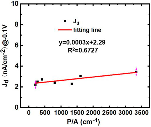
FIGURE 10. Dark current density versus P/A.

TABLE 2. Parameters used in calculation [13].
Noise Electron
The noise electron of InGaAs FPAs contains PDA noise, ROIC noise, and the combined noise of PDAs and ROIC. The PDA noise mainly comes from thermal noise and the shot noise of dark current. The ROIC noise electron and FPA noise electron are measured under CDS mode and non-CDS mode, respectively. The results show the ROIC noise electron is 42 e−, and the InGaAs FPA noise electron is 72 e− under non-CDS mode, while the ROIC noise electron is 20 e− and the InGaAs FPA noise electron is 48 e− under CDS mode. The thermal noise electron Nthermal and the shot noise electron Nin,shot were calculated according to Eq. 6 and Eq. 7 [13], respectively.
where q is the electric quantity, k is the Boltzmann constant, T is temperature, Id is the dark current, Rd is the pixel resistance, and Tint is the integration time.
The calculation results of the thermal noise and shot noise of dark current are about 14e− and 11e−, respectively. The PDA noise electrons are 25 e− at room temperature. Compared with the actual measurement results in Table 3, it is revealed that PDA noise is the main contribution of FPA noise under CDS mode, while the ROIC noise is the main contribution of FPA noise under non-CDS mode operation.

TABLE 3. Noise measurement results of FPA and ROIC.
Detectivity D*
The detectivity D* is up to 1.1 × 1013 cm⋅Hz1/2/W and the signal noise ratio (SNR)is 64dB under CDS mode. But under non-CDS mode the detectivity D* is 4.2 × 1012 cm⋅Hz1/2/W, and the SNR is 52 dB. According to the previous analysis of readout noise electron, the FPA readout noise electron under CDS mode is lower than that under non-CDS mode, which causes the SNR under CDS mode to be larger than that under non-CDS mode. Therefore, as shown in Eq. 7, the D* is higher under CDS mode than that under non-CDS mode. The ROIC noise is the main reason that causes the SNR and the detectivity D* to be lower under non-CDS mode.
where Rv is the response voltage, Vn is the noise voltage, Ad is the photo-sensitive pixel area, and Δf is the noise equivalent bandwidth.
Conclusion
In summary, a high-performance 15 μm 1,280 × 1,024 InGaAs PIN short wave infrared detector was fabricated by optimizing the EPI material quality and Zn diffusion processing. The results indicate that the dark current is as low as 2.25 nA/cm−2 at room temperature, and the theoretical calculation datum of dark current shows that the diffusion current is the main contribution of dark current. Under CDS mode operation, the response non-uniformity of the megapixel FPA is 4.2%, the operability is more than 99.9%, the detectivity D* is up to 1.1 × 1013 cm⋅Hz1/2/W, the SNR is 64dB, and the main contribution of FPA noise comes from PDAs whose noise electron is 25 e−. Owing to larger noise from ROIC under non-CDS mode, the detectivity is 4.2 × 1012 cm⋅Hz1/2/w, and the SNR is 52dB. The test results show the ROIC noise is the main cause of the SNR and lower detectivity D* under non-CDS mode.
Data Availability Statement
The original contributions presented in the study are included in the article/Supplementary Material, further inquiries can be directed to the corresponding author.
Author Contributions
J-XZ: development and design of methodology, original draft writing and modification. WW: mask design, data curation. Y-LS: datum analyses and supervision, paper modification and verification, Z-BL: investigation, H-FY, Z-PH and R-YH: provision of study material, HZ: data curation, CL: visualization, HZ: format analysis, X-YY: datum discussion.
Conflict of Interest
Author JZ, WW was employed by the Shanxi Guohui Optoelectronic Technology Com LTD.
The remaining authors declare that the research was conducted in the absence of any commercial or financial relationships that could be construed as a potential conflict of interest.
Publisher’s Note
All claims expressed in this article are solely those of the authors and do not necessarily represent those of their affiliated organizations, or those of the publisher, the editors, and the reviewers. Any product that may be evaluated in this article, or claim that may be made by its manufacturer, is not guaranteed or endorsed by the publisher.
Acknowledgments
This work was supported in part by the Yunnan provincial major science and technology special foundation (2018ZI002).
References
1. Gao HJ, Zhou YH. Recent Progresses in InGaAs Visible/short Wavelength Infrared Focal Plane Array Detectors[J]. Infrared Laser Eng (2007) 36(4):431–4.
2. Shao XM, Gong HM, Li X, Fang JX, Tang HJ, Li T, et al. Development of High Performance Short-Wave Infrared InGaAs Focal Plane Detectors[J]. Infrared Tech (2016) 38(8):629–35.
3. Cao Y, Jin WQ, Wang X, Xu C Development in Shortwave Infrared Focal Plane Array and Application[J]. Infrared Tech (2009) 31(2):63–8.
4. Hansen MP, Malchow DC, Overview of SWIR Detectors, Cameras, and Applications[C]. In: Thermosense International Society for Optics and Photonics (2008) 6939. p. 0I–1.
5. Huang S, O'Grady M, Groppe JV, Ettenberg MH, Brubaker RM. A Customizable Commercial Miniaturized 320×256 Indium Gallium Arsenide Short Wave Infrared Camera[C]. In: Conference on Infrared Systems and Photoelectronic Technology; October, 2004; Denver, CO(US) (2004). doi:10.1117/12.560058
6. Martin T, Brubaker R, Dixon P, Gagliardi MA, Sudol T. 640x512 InGaAs Focal Plane Array Camera for Visible and SWIR imaging[C]. Proceedings of the Infrared Techn. Applications XXXI International Society for Optics and Photonics; May 2005; Orlando, Florida, United States (2005)
7. Liu JH, Gao XJ, Zhou X. Developments and Perspectives of SWIR InGaAs Focal Plane Arrays [J]. Semiconductor optoelectronics (2015)(05) 10–5.
8. Li X, Shao XM, Li T, Cheng ZC, Huang ZC, Huang SL, et al. Research Progress of Short Wave Infrared InGaAs Focal Plane Detectors[J]. Infrared Laser Engineering (2020) 01:64–71. doi:10.3788/IRLA202049.0103006
9. Macdougal M, Geske J, Wang C, Liao S, Getty J, Holmes A. Low Dark Current in Ga as Detector Arrays for Night Vision and Astronomy[C]. In: Proceedings of the Infrared Technology & Applications XXXV; May 2009; Orlando, Florida, United States (2009). doi:10.1117/12.820377
10. Fraenkel R, Berkowicz E, Bykov L, Dobromislin R, Elishkov R, Giladi A, et al. High Definition 10μm Pitch in Ga as Detector with Asynchronous Laser Pulse Detection Mode[C]. In: Proceedings of the Infrared Technology & Applications XLII; May 2016; Baltimore, Maryland, United States (2016). doi:10.1117/12.2222762
11. Hood AD, Macdougal MH, Follman D, Manzo J, Geske JC. Large-format InGaAs Focal Plane Arrays for SWIR Imaging[C]. In: Proceedings Volume 8353, Infrared Technology and Applications XXXVIII; May 2012; Baltimore, Maryland, United States. Spie Defense, Security, & Sensing (2012). doi:10.1117/12.921475
12. Dewames R, Littleton R, Witte K, Wichman A, Bellotti E, Pellegrino J. Electro-Optical Characteristics of P+ N In0.53 Ga0.47 as Hetero-Junction Photodiodes in Large Format Dense Focal Plane Arrays[J]. J Electron Mater (2015) 44:2813–22. doi:10.1007/s11664-015-3706-8
13. Cao GQ, Basic Research on Application of High Sensitivity Planar InGaAs Short Wave Infrared Detector [D] 2016(5):96–100.
14. Yuan P, Boisvert JC, Karam N. Low-dark Current 1024x1280 InGaAs PIN Arrays[C]. In: Proceedings of the Infrared Technology & Applications XLInternational Society for Optics and Photonics; June 2014; Baltimore, Maryland, United States (2014). doi:10.1117/12.2053999
Keywords: InGaAs SWIR FPA, readout integrated circuit, noise electron, dark current, quantum efficiency, correlated double sampling
Citation: Zhang J-X, Wang W, Li Z-B, Ye H-F, Huang R-Y, Hou Z-P, Zeng H, Zhu H-x, Liu C, Yang X-Y and Shi Y-L (2021) Development of a High Performance 1280×1024 InGaAs SWIR FPA Detector at Room Temperature. Front. Phys. 9:678192. doi: 10.3389/fphy.2021.678192
Received: 09 March 2021; Accepted: 20 September 2021;
Published: 25 October 2021.
Edited by:
Jun Wang, University of Electronic Science and Technology of China, ChinaReviewed by:
Haimei Gong, Shanghai Institute of Technical Physics, ChinaZhenhua Ye, Shanghai Institute of Technical Physics (CAS), China
Copyright © 2021 Zhang, Wang, Li, Ye, Huang, Hou, Zeng, Zhu, Liu, Yang and Shi. This is an open-access article distributed under the terms of the Creative Commons Attribution License (CC BY). The use, distribution or reproduction in other forums is permitted, provided the original author(s) and the copyright owner(s) are credited and that the original publication in this journal is cited, in accordance with accepted academic practice. No use, distribution or reproduction is permitted which does not comply with these terms.
*Correspondence: Yan-Li Shi, eWxzaGlrbUBob3RtYWlsLmNvbQ==