 Yunxia Sui1
 Pan Hu
 Fanxin Liu
- 1Department of Applied Physics, Zhejiang University of Technology, Hangzhou, China
- 2Ming Hsieh Department of Electrical and Computer Engineering, University of Southern California, Los Angeles, CA, United States
Sub-wavelength strongly confined electromagnetic field induced by surface plasmon resonance offers a promising method to enhance the light-matter interactions, which has wide applications in the fields of enhanced spectroscopy, photovoltaic conversion, and photocatalysis. For periodic metal nanostructures, the localized surface plasmon resonance (LSPR) can couple with the long-range diffractive interaction, causing a narrow linewidth. Here, we report a new family of plasmonic nanostructure fabricated through nanoimprint lithograph, which enables completely uniform, reproducible, and low-cost Au nanofinger multimer arrays with high aspect ratio at the manufacturing scale. Through adjusting the lattice spacing and the angle of incident light, the different collective coupling strengths between the diffraction modes and the LSPR of trimer or pentamer Au nanofingers arrays are observed experimentally by angle-resolved reflection spectroscopy. According to the numerical simulation based on the finite element method, the dynamic evolution of collective coupled modes is demonstrated. The typical surface charge distribution and electric field distribution of the coupled dipole resonance show a significant electromagnetic field enhancement. By adjusting the height of nanofingers, lattice spacing and gap size of adjacent nanofingers, the feasibility of the coupled modes is further investigated. This work provides an excellent candidate for the localization of light as chip-scale plasmonic devices.
1 Introduction
Localized surface plasmon resonance (LSPR) induced by noble metal nanostructures can concentrate light into sub-wavelength regions to generate strong near-field enhancement [1–4], which enables many significant applications in the field of nanophotonics, such as enhanced spectroscopy [5–8], photovoltaic conversion [9,10], photocatalysis [11], and other enhanced light-matter interactions [12]. Compared to isolated nanoparticles, multiple nanoparticles or metallic arrays of nanostructures can form hybrid modes due to the interaction between the individual optical modes overlapping in spatial and spectral space, which greatly enriches the manipulation of localized optical fields and further improves optical performances [13,14]. For instance, nanoparticles with sub-nanometer gaps can produce exponentially enhanced localized electric fields owing to the near-field coupling [15,16]. The destructive interference between the narrow sub-radiant mode and the broad supper-radiant mode can result in Fano resonance, which shows vary narrow linewidth that can be used to improve the refractive index sensing [17,18]. In addition, for plasmonic lattice structures, a geometric resonance arises when the LSPR wavelength of a single nanostructure is commensurate with the periodicity of the lattice arrays, which leads to a dramatic modification of the extinction spectrum [19–23]. The periodic metal nanostructures featured with good uniformity and repeatability will support a higher-quality nanocavity due to the coupling between the LSPR and the long-range diffractive modes, which is highly useful for light harvesting [24–27]. However, in plasmonic lattice arrays, it is found that the mismatch of environmental refractive index between the upper interface in contact with air and the lower interface in contact with substrate will decrease the coupling efficiency of light in free space [28]. To solve this problem, nearly free-standing metal nanoparticle arrays are preferred by reducing the spatial overlap between the substrate and the enhanced field, thus, allowing for a larger spatial area of field enhancement and improved refractive index sensitivity [29]. More recently, special suspended elevated metallic nanoparticle arrays, such as mushroom and bowtie arrays with dielectric pillars are fabricated, which presents better performance in refractive index sensing [22,30–32]. However, it is still a challenge for conventional physical fabrication methods to fabricate high uniform, reproducible, and low-cost nanoarrays with a high aspect ratio at the manufacturing scale due to the lithography and etching process limitations.
In this work, we report new plasmonic lattice arrays of Au nanofingers trimer and pentamer arrays fabricated by nanoimprint lithograph, in which the height of supporting dielectric pillars can reach up to 600 nm. This well-developed nanofingers array with a high aspect ratio is valuable for light harvesting. As compared to conventional physical fabrication, the height of our nanofingers is over half of the wavelength, which can effectively support the lattice mode of periodic arrays. Furthermore, our methods have the benefits of low-cost, high repeatability, and large area and, thus, are preferred to be the platform to study nanophotonics. Through adjusting the angle of incident light and lattice spacing, we successfully observed the collective coupling between the LSPR and periodic diffraction modes by angle-resolved reflection spectroscopy measurements. Furthermore, we explored the dynamic evolution and structural geometry parameters dependence on collective coupling modes in plasmonic lattice by numerical simulations. It is noted that our periodic Au nanofingers are flexible and can be collapsed to each other. In addition, the gap size of adjacent nanofingers can be precisely controlled by pre-deposited dielectric films. The proposed approach opens novel opportunities for the engineering of metal nanostructure arrays with optimized performance for spectroscopic and sensing applications.
2 Results and discussion
The high-density trimer and pentamer arrays of nearly free-standing flexible nanofingers are firstly fabricated by our well-developed nanoimprint lithography (NIL) and reactive-ion etching based on polymer materials (PDMS), which enables a high aspect ratio at the manufacturing scale [33,34]. The typical height and diameter of each nanofinger are 600 nm and 70 nm, respectively. The gap size of adjacent nanofingers is 130 nm. In addition, two square lattice arrays with different periods of 670 nm and 5 μm are fabricated. Subsequently, a 50 nm Au layer is deposited onto the top of nanofingers by e-beam evaporation. Figure 1 shows the scanning electron microscopy (SEM). The results show that the trimer and pentamer Au nanofinger arrays with different lattice constant have high-quality morphology, which is consistent with the design. It is noted that the nanofingers with adjustable configuration and geometric structure parameters can be finely defined by initial electron-beam lithography (EBL) and reproduced faithfully by NIL.
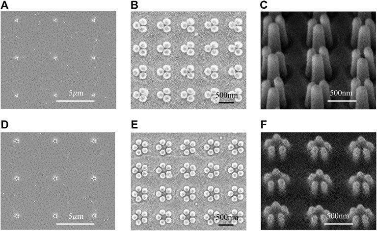
FIGURE 1. SEM images of trimer or pentamer Au nanofinger arrays. (A) Top-view SEM image of trimer Au nanofinger arrays with lattice constant of 5 μm. Scale bar: 5 μm. (B) Top-view SEM image of trimer Au nanofinger arrays with lattice constant of 670 nm. Scale bar: 500 nm. (C) Oblique-view SEM image of magnified trimer Au nanofinger arrays with 500 nm scale bar. (D–F) Corresponding SEM images for pentamer Au nanofinger arrays.
The angle-resolved reflection spectra are first measured to explore the coupling between the LSPR and periodic diffraction modes for trimer and pentamer Au nanofinger arrays with lattice constant of 5 μm, as shown in Figure 2. Here, the intensity of the reflectance is normalized in terms of the intensity of the peak. The results indicate that the reflection peak position is almost unchanged when the angle of incident light (θ) is changed from −30° to 30° for both trimer and pentamer nanostructures. It can be ascribed to weak coupling between the LSPR modes of single nanofingers and periodic diffraction modes. In order to better understand the underlying physics, we have simulated the corresponding extinction spectra of isolated nanofinger multimers based on the finite element method. The geometrical parameters are consistent with the experimental design. The permittivity of Au is from the COMSOL built-in material library, and the refractive index of PDMS is set as 1.41. In simulations, a plane wave with x-direction polarization irradiates normally along the negative z-axis direction, and trimer or pentamer nanofinger arrays are surrounded by a perfect matched layer condition. The results show a dominant extinction peak at 540 nm for trimer and at 555 nm for pentamer, as shown in Figures 2B and D. As compared to experimental measurements, there is a little difference in resonant wavelength, which might be attributed to the geometry deviation between experiments and simulations. Considering the gap size of adjacent nanofingers is 130 nm, the near-field coupling effect between adjacent nanofingers is weak. Consequently, the typical surface charge distributions of trimer or pentamer nanofingers at the resonant excitation all present the isolated dipole resonant modes with the same orientations of dipole moment, which are parallel with the polarized direction of incident light.
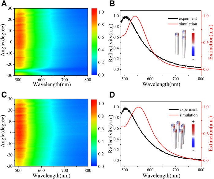
FIGURE 2. Experimentally measured and numerically simulated reflection spectra of trimer or pentamer Au nanofinger arrays with lattice constant of 5 μm. (A) Experimentally measured angle-resolved reflection spectra of trimer Au nanofinger arrays. (B) Experimentally measured reflection spectra and numerically simulated extinction spectra of trimer Au nanofinger arrays with normal incidence. Inset: corresponding charge distribution with resonant excitation. (C and D) Corresponding data for pentamer Au nanofinger arrays.
To further explore the effect of lattice constant on the coupling strength, the trimer or pentamer Au nanofinger arrays with small lattice constant of 670 nm are studied, as shown in Figure 3. Different from nanofinger arrays with larger lattice constant of 5 μm, the results of angle-resolved reflection spectra of nanofinger arrays with lattice constant of 670 nm present obvious incident angle dependence. For trimer arrays shown in Figures 3A and B, the reflection peak is blue and shifted gradually with the angle of incidence increasing from 0° to 30°. In the meantime, the peak width at half height becomes narrower, which means the quality of resonant mode increased, and a dip appeared at around 600 nm in the reflection spectra. For pentamer arrays, as shown in Figures 3C and D, except for a similar phenomenon in the experimentally measured angle-resolved reflection spectra, the resonant peak shows a narrower peak width at half height, which means a strong coupling strength between the LSPR modes of single nanofingers and the periodic diffraction modes. To demonstrate the collective coupling effects, numerical simulations with 0°, 15°, and 25° incident angle are performed. The lattice constant is set as 670 nm. The periodic boundary conditions are used in x and y directions, and a perfectly matched layer condition is imposed at the boundaries along z directions. Other geometric and material parameters are the same as mentioned before. As shown in Figure 4A, the simulated reflection peak shows a blue shift when the angle of incidence increases from 0 to 30°, which is consistent with experimental measurements. The simulated reflection spectrum also shows an obvious Fano line type around 670 nm, which is related to the strong coupling between the LSPR and the long-range diffractive modes [35]. The position of the dip is associated with Rayleigh cut-off wavelength (
where
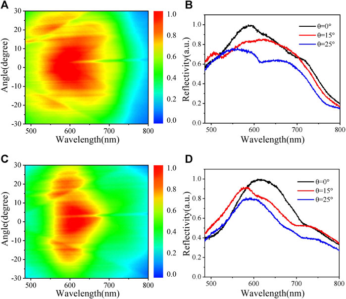
FIGURE 3. Experimentally measured angle-resolved reflection spectra of trimer or pentamer Au nanofinger arrays with lattice constant of 670 nm. (A) Reflection spectra of trimer Au nanofinger arrays for the incidence angle varied from -30° to 30°. (B) Experimental reflection spectra of trimer Au nanofinger arrays at the incidence angle of 0°, 15° and 25°, as selected from (A). (C and D) Corresponding data for pentamer Au nanofinger arrays.
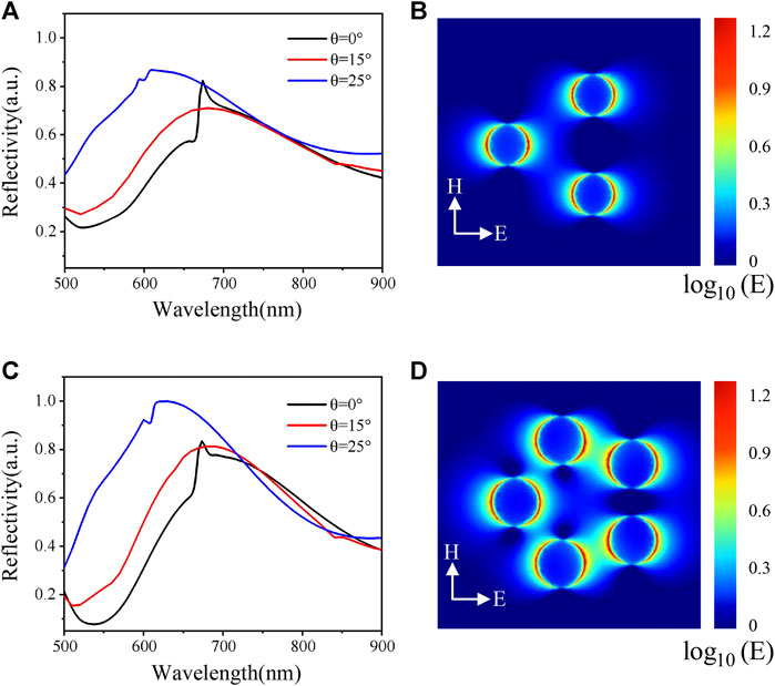
FIGURE 4. Numerically simulated reflection spectra of trimer or pentamer Au nanofinger arrays with lattice constant of 670 nm. (A) Simulated reflection spectra of Au nanofinger trimer arrays at the incidence angle of 0°, 15°, and 25°. (B) Electric field distribution for the trimer Au nanofinger arrays with normal incidence at peak of 670 nm. (C and D) Corresponding data for pentamer Au nanofinger arrays.
When the incident light wavelength coincides with the Rayleigh cutoff wavelength, the diffracted wave will move along the substrate surface at a swept angle to interact with the nanoparticles in the array. The Rayleigh cutoff wavelength is equal to the lattice constant when normal incidence is applied, so the value will show anomalously sharp resonant peaks at wavelengths near the lattice constant. As shown in Figure 4B, the electric field distribution at the Rayleigh cutoff wavelength shows an obvious enhancement, which is very beneficial for the applications in enhancing the light-matter interactions. As for pentamer arrays with lattice constant of 670 nm, the simulated angle-resolved reflection spectra and electric field distribution all present collective coupling resonant characteristics, as shown in Figures 4C and D.
Finally, we further studied the dynamic evolution and structural geometry parameters dependence of collective coupling modes. As shown in Figure 5A, the reflection spectra of Au nanofingers trimer arrays with normal incidence are simulated, in which the height of the PDMS pillar is set as 100, 300, and 600 nm, and the period and gap size are set as 670 nm and 130 nm, respectively. The results show that the height of PDMS pillars strongly affected the reflection spectra of the plasmonic lattices, where the short pillars can hard support the long-range diffractive interaction so that the Fano line types will disappear. This is because of the mismatch of the environmental refractive index between the upper interface in contact with air and the lower interface in contact with substrate, which decreases the coupling in free space. In addition, the tunability of our well-designed nanostructures can be easily achieved in the visible region from 500 nm to 900 nm by changing the period of nanofingers. As shown in Figure 5B, with the increase of the period when other parameters are fixed, the wavelength of Rayleigh anomalies increases. It is worth noting that the nanofingers are flexible. When the samples are soaked in ethanol and air-dried, the adjacent flexible nanofingers collapse to form the physically touched arrays due to the capillary force. In addition, the gap size can be precisely controlled by pre-deposited dielectric films, in which the gap size of adjacent nanofingers is defined as twice of the dielectric films. Therefore, we simulated the reflection spectra with different gap sizes of adjacent nanofingers. As shown in Figure 5C, the reflection peaks with higher quality factors can be obtained by narrowing the gap sizes when other parameters remain unchanged. It is believed that this approach has great application potential in plasmonic enhanced devices.
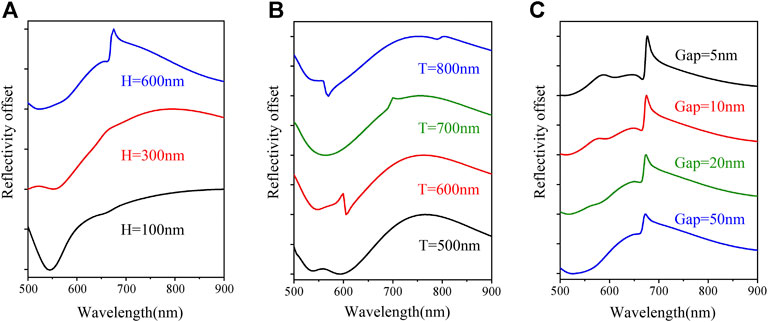
FIGURE 5. Numerically simulated reflection spectra of trimer Au nanofinger arrays with different geometric structure parameters at normal incidence. (A) Simulated reflection spectra of nanofingers with different heights, and the period T and gap size are set as 670 nm and 130 nm, respectively. (B) Simulated reflection spectra of nanofingers with different lattice constants, and the height H and gap size are set as 600 nm and 130 nm, respectively. (C) Simulated reflection spectra of nanofingers with different gap sizes of adjacent nanofingers, and the period T and height H are set as 670 nm and 600 nm, respectively.
3 Conclusion
In summary, we developed a high uniform, reproducible, and low-cost Au ordered nanofingers arrays by nanoimprint lithograph, in which the height of supporting dielectric pillars can reach up to 600 nm. The collective coupling between diffraction patterns and LSPR of single Au nanofingers based on trimer and pentamer Au nanofinger arrays were experimental observed through the angle-resolved reflection spectra. We further investigated the dynamic evolution of collective coupling modes in the plasmonic lattice by adjusting the height of nanofingers and lattice spacing and gap size of adjacent nanofingers in numerical simulations. It can provide new opportunities for engineering metal nanoarrays with optimized performance for spectroscopic and sensing applications.
Data availability statement
The original contributions presented in the study are included in the article/Supplementary Material; further inquiries can be directed to the corresponding authors.
Author contributions
FL and WW conceived the idea. YS, DP, and GS performed the numerical simulations. GS, ZJ, and QS performed the experimental measurements. PH carried out the sample preparation. FL, GS, and YS prepared the manuscript. All authors discussed the data presented in the manuscript.
Funding
This study was funded by the National Natural Science Foundation of China (Nos. 11974015 and 11574270) and the Natural Science Foundation of Zhejiang Province (No. LZ22A040008).
Conflict of interest
The authors declare that the research was conducted in the absence of any commercial or financial relationships that could be construed as a potential conflict of interest.
Publisher’s note
All claims expressed in this article are solely those of the authors and do not necessarily represent those of their affiliated organizations, or those of the publisher, the editors, and the reviewers. Any product that may be evaluated in this article, or claim that may be made by its manufacturer, is not guaranteed or endorsed by the publisher.
References
1. Halas NJ, Lal S, Chang W, Link S, Nordlander P. Plasmons in strongly coupled metallic nanostructures. Chem Rev (2011) 111:3913–61. doi:10.1021/cr200061k
2. Schuller JA, Barnard ES, Cai W, Jun YC, White JS, Brongersma ML. Plasmonics for extreme light concentration and manipulation. Nat Mater (2010) 9:193–204. doi:10.1038/nmat2630
3. Li J, Zhang Y, Ding S, Panneerselvam R, Tian Z. Core–shell nanoparticle-enhanced Raman spectroscopy. Chem Rev (2017) 117:5002–69. doi:10.1021/acs.chemrev.6b00596
4. Barnes WL, Dereux A, Ebbesen TW. Surface plasmon subwavelength optics. Nature (London) (2003) 424:824–30. doi:10.1038/nature01937
5. Lim D, Jeon K, Kim HM, Nam J, Suh YD. Nanogap-engineerable Raman-active nanodumbbells for single-molecule detection. Nat Mater (2010) 9:60–7. doi:10.1038/nmat2596
6. Ding S, Yi J, Li J, Ren B, Wu DY, Panneerselvam R, et al. Nanostructure-based plasmon-enhanced Raman spectroscopy for surface analysis of materials. Nat Rev Mater (2016) 1:16021. doi:10.1038/natrevmats.2016.21
7. Yu P, Besteiro LV, Huang Y, Wu J, Fu L, Tan HH, et al. Broadband metamaterial absorbers. Adv Opt Mater (2019) 7:1800995. doi:10.1002/adom.201800995
8. Olesiak-Banska J, Waszkielewicz M, Obstarczyk P, Samoc M. Two-photon absorption and photoluminescence of colloidal gold nanoparticles and nanoclusters. Chem Soc Rev (2019) 48:4087–117. doi:10.1039/c8cs00849c
9. Atwater HA, Polman A. Plasmonics for improved photovoltaic devices. Nat Mater (2010) 9:205–13. doi:10.1038/nmat2629
10. Saliba M, Zhang W, Burlakov VM, Stranks SD, Sun Y, Ball JM, et al. Plasmonic-induced photon recycling in metal halide perovskite solar cells. Adv Funct Mater (2015) 25:5038–46. doi:10.1002/adfm.201500669
11. Wang Q, Domen K. Particulate photocatalysts for light-driven water splitting: Mechanisms, challenges, and design strategies. Chem Rev (2020) 120:919–85. doi:10.1021/acs.chemrev.9b00201
12. Luo Y, Shepard GD, Ardelean JV, Rhodes DA, Kim B, Barmak K, et al. Deterministic coupling of site-controlled quantum emitters in monolayer WSe2 to plasmonic nanocavities. Nat Nanotech (2018) 13:1137–42. doi:10.1038/s41565-018-0275-z
13. Prodan E, Radloff C, Halas NJ, Nordlander P. A hybridization model for the plasmon response of complex nanostructures. Science (American Association for the Advancement of Science) (2003) 302:419–22. doi:10.1126/science.1089171
14. Chu Y, Schonbrun E, Yang T, Crozier KB. Experimental observation of narrow surface plasmon resonances in gold nanoparticle arrays. Appl Phys Lett (2008) 93:181108. doi:10.1063/1.3012365
15. Xu H, Bjerneld EJ, Käll M, Börjesson L. Spectroscopy of single hemoglobin molecules by surface enhanced Raman scattering. Phys Rev Lett (1999) 83:4357–60. doi:10.1103/PhysRevLett.83.4357
16. Chirumamilla M, Toma A, Gopalakrishnan A, Das G, Zaccaria RP, Krahne R, et al. 3D nanostar dimers with a sub-10-nm gap for single-/few-molecule surface-enhanced Raman scattering. Adv Mater (2014) 26:2353–8. doi:10.1002/adma.201304553
17. Sonnefraud Y, Verellen N, Sobhani H, Vandenbosch GA, Moshchalkov VV, Van Dorpe P, et al. Experimental realization of subradiant, superradiant, and Fano resonances in ring/disk plasmonic nanocavities. ACS nano (2010) 4:1664–70. doi:10.1021/nn901580r
18. Hentschel M, Saliba M, Vogelgesang R, Giessen H, Alivisatos AP, Liu N. Transition from isolated to collective modes in plasmonic oligomers. Nano Lett (2010) 10:2721–6. doi:10.1021/nl101938p
19. Auguié B, Barnes WL. Collective resonances in gold nanoparticle arrays. Phys Rev Lett (2008) 101:143902–. doi:10.1103/PhysRevLett.101.143902
20. Kravets VG, Schedin F, Grigorenko AN. Extremely narrow plasmon resonances based on diffraction coupling of localized plasmons in arrays of metallic nanoparticles. Phys Rev Lett (2008) 101:087403–. doi:10.1103/PhysRevLett.101.087403
21. Zhou W, Odom TW. Tunable subradiant lattice plasmons by out-of-plane dipolar interactions. Nat Nanotech (2011) 6:423–7. doi:10.1038/nnano.2011.72
22. Shen Y, Zhou J, Liu T, Tao Y, Jiang R, Liu M, et al. Plasmonic gold mushroom arrays with refractive index sensing figures of merit approaching the theoretical limit. Nat Commun (2013) 4:2381–. doi:10.1038/ncomms3381
23. Boddeti AK, Guan J, Sentz T, Juarez X, Newman W, Cortes C, et al. Long-range dipole–dipole interactions in a plasmonic lattice. Nano Lett (2022) 22:22–8. doi:10.1021/acs.nanolett.1c02835
24. Wang D, Guan J, Hu J, Bourgeois MR, Odom TW. Manipulating light–matter interactions in plasmonic nanoparticle lattices. Acc Chem Res (2019) 52:2997–3007. doi:10.1021/acs.accounts.9b00345
25. Abass A, Rodriguez SR, Gómez Rivas J, Maes B. Tailoring dispersion and eigenfield profiles of plasmonic surface lattice resonances. ACS Photon (2014) 1:61–8. doi:10.1021/ph400072z
26. Roiguez SRK, Abass A, Maes B, Janssen OTA, Vecchi G, Gómez Rivas J. Coupling bright and dark plasmonic lattice resonances. Phys Rev X (2011) 1:021019. doi:10.1103/PhysRevX.1.021019
27. Kataja M, Hakala TK, Julku A, Huttunen MJ, Van Dijken S, Törmä P. Surface lattice resonances and magneto-optical response in magnetic nanoparticle arrays. Nat Commun (2015) 6:7072. doi:10.1038/ncomms8072
28. Tam F, Moran C, Halas N. Geometrical parameters controlling sensitivity of nanoshell plasmon resonances to changes in dielectric environment. J Phys Chem B (2004) 108:17290–4. doi:10.1021/jp048499x
29. Dmitriev A, Hägglund C, Chen S, Fredriksson H, Pakizeh T, Kall M, et al. Enhanced nanoplasmonic optical sensors with reduced substrate effect. Nano Lett (2008) 8:3893–8. doi:10.1021/nl8023142
30. Hatab NA, Hsueh C, Gaddis AL, Retterer ST, Li JH, Eres G, et al. Free-standing optical gold bowtie nanoantenna with variable gap size for enhanced Raman spectroscopy. Nano Lett (2010) 10:4952–5. doi:10.1021/nl102963g
31. Near R, Tabor C, Duan J, Pachter R, El-Sayed M. Pronounced effects of anisotropy on plasmonic properties of nanorings fabricated by electron beam lithography. Nano Lett (2012) 12:2158–64. doi:10.1021/nl300622p
32. Yan N, Liu X, Zhu J, Zhu Y, Jiang W. Well-ordered inorganic nanoparticle arrays directed by block copolymer nanosheets. ACS nano (2019) 13:6638–46. doi:10.1021/acsnano.9b00940
33. Liu F, Song B, Su G, Liang O, Zhan P, Wang H, et al. Molecule sensing: Sculpting extreme electromagnetic field enhancement in free space for molecule sensing (small 33/2018). Small (2018) 14:1870152. doi:10.1002/smll.201870152
34. Song B, Yao Y, Groenewald RE, Wang Y, Liu H, Wang Y, et al. Probing gap plasmons down to subnanometer scales using collapsible nanofingers. ACS nano (2017) 11:5836–43. doi:10.1021/acsnano.7b01468
Keywords: plasmonic lattice, long-range diffractive interaction, localized surface plasmon resonance, nanofinger arrays, angle-resolved reflection spectroscopy
Citation: Sui Y, Hu P, Pan D, Jiang Z, Song Q, Su G, Wu W and Liu F (2022) Long-range interference of localized electromagnetic field enhancement in plasmonic nanofinger lattices. Front. Phys. 10:951944. doi: 10.3389/fphy.2022.951944
Received: 24 May 2022; Accepted: 08 August 2022;
Published: 08 September 2022.
Edited by:
Cong Liu, Nokia Bell Labs, United StatesReviewed by:
Xiangzhi Li, Los Alamos National Laboratory (DOE), United StatesYize Liang, Huazhong University of Science and Technology, China
Copyright © 2022 Sui, Hu, Pan, Jiang, Song, Su, Wu and Liu. This is an open-access article distributed under the terms of the Creative Commons Attribution License (CC BY). The use, distribution or reproduction in other forums is permitted, provided the original author(s) and the copyright owner(s) are credited and that the original publication in this journal is cited, in accordance with accepted academic practice. No use, distribution or reproduction is permitted which does not comply with these terms.
*Correspondence: Guangxu Su, Z3hzdUB6anV0LmVkdS5jbg==; Fanxin Liu, bGl1ZmFueGluQHpqdXQuZWR1LmNu