- 1Laboratory of Superconducting Quantum Information Processing, School of Integrated Circuits, Tsinghua University, Beijing, China
- 2Beijing National Research Center for Information Science and Technology, Beijing, China
- 3Beijing Innovation Center for Future Chips, Tsinghua University, Beijing, China
This paper presents a design and fabrication process of a cryogenic multiplexing control chip (MCC) for superconducting quantum computers. The working temperature of MCC can be 10 ∼ 30 mK, because it could be integrated with quantum processor in the same package. With a multiplexing ratio of 1:4 and designed working frequency 4–8 GHz, the MCC is a non-reciprocity device which consisted of bandpass filters and isolators, which are based on tunable inductor bridges (TIB). The MCC chip size is 6 × 6 mm2 and includes λ/2 coplanar waveguides resonators, superconducting quantum interference device arrays, capacitors, low pass filters, baluns and bias lines. Adopting self-aligned process of Josephson junctions, the fabrication of MCC constitutes four lithography masks. The modular design of MCC could facilitate the development of large-scale superconducting quantum computers.
1 Introduction
Superconducting quantum computers are typically operated by microwave control and dispersive readout of transmon qubits in a circuit quantum electrodynamic architecture [1–8]. As the quantum processors scale up relentlessly, the requisite number of microwave control lines increases linearly with the number of the qubits [9,10]. By adopting frequency-domain multiplexing dispersive readout of qubits, a single readout line can be used to deal with multiple probe tones, thus mitigating the demand of microwave cable chains in the readout modules [11,12]. Fitting enough microwave control lines at the base temperature region of a dilution refrigerator is one eventual bottleneck associated with building a scalable quantum computer [13–15]. The bottleneck has been aimed to be resolved by several approaches, such as cryogenic complementary metal oxide semiconductors (cryo-CMOS) device [15–18], photonic link (PL) [19], single flux quantum (SFQ) digital logic [20,21]. Our group has presented a proposal for a cryogenic multiplexing control chip (MCC), which is a nonreciprocal device and composed of tunable inductor bridges (TIB) based on SQUID arrays [22]. There are XY and Z two kinds single-qubit control operations of superconducting quantum processor. The MCC chip can support the XY multiplexing frequency control. In addition, the MCC can separate different frequencies of superconducting qubits into different channels with very low crosstalk (−80 dB) and the qubits are protected from interference. The MCC is to be working at a temperature of 20 mK, and could be directly integrated with the quantum processor in one package [22] or removed separately from the cryogenic system and act as an independent chip. Although there were demonstrations for cryo-CMOS, PL and SFQ approaches, however, an experimental realization for MCC is still in need. The design and fabrication of MCC would be a substantial challenge with the increasing number of superconducting quantum interference device (SQUID) arrays and the complicity of interconnections among them.
In this work, a design and fabrication process for a cryogenic on-chip MCC working at 20 mK with multiplex ratio of 1:4 and working frequency 4–8 GHz is presented. The electric circuit and the layout design are described. The band pass filters (BPFs) are implemented by λ/2 coplanar waveguides (CPW) resonators and a set of cosine and sine bias lines are shared by four tunable superconducting isolators. The MCC footprint is 6 × 6 mm2 and the fabrication process has been carried out by using a set of four lithographical masks based on a self-aligned technique for Josephson junctions (JJs).
In the following, Section 2 presents circuit and layout design of MCC. Section 3 gives the fabrication process and results of MCC. The paper is concluded in Section 4.
2 Circuit and layout design
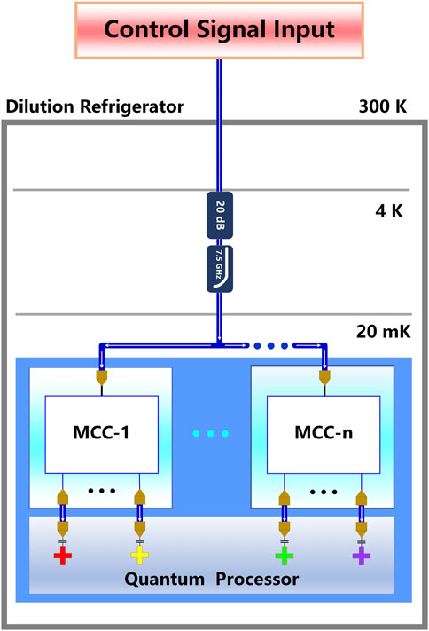
A sketch of MCCs and their utilization in superconducting quantum computer is depicted in Figure 1. The input control multiplexed signal is distributed to a series of MCCs (MCC-1, … , MCC-n). Each MCC is composed of BPFs and tunable superconducting isolators [22]. The frequency-domain demultiplexed microwave signals are routed to the XY control ports of superconducting qubits on a quantum processor. The colorful crosses in the quantum processor mean qubits with different frequencies. Because the MCC is based on frequency domain multiplexing, the set of qubits being controlled by a single MCC chip should be tuned to different frequencies in according to the frequency spectrum of the MCC.
The electric circuit of MCC with multiplex ratio 1:4 is given in Figure 2A. Various kinds of BPFs, e.g., Bessel BPF, Butterworth BPF and Chebyshev BPF of MCC were simulated [22]. Here, the BPFs are implemented by λ/2 CPW resonators. Therefore, MCC is composed of λ/2 CPW resonators and superconducting isolators, which consist of nonlinear inductors and capacitors. Each nonlinear inductor is comprised of a SQUID array [22,23]. The resonators in different colors implement BPFs of different central frequencies for a coarse selection of band-passing frequency.
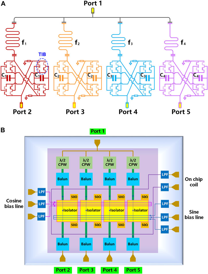
FIGURE 2. Electric circuit and schematic layout of MCC. (A) Diagrammatic electric circuit of MCC with multiplex ratio 1:4. The resonators in different colors implement BPFs of different central frequencies. (B) Schematic layout of MCC. The λ/2 CPW resonators are connected with baluns. Then the microwave signals enter the superconducting tunable isolators and exit to baluns before outputting to Ports 2–5.
In order to adjust the center frequency of MCC more efficiently, a tricky challenge to the layout design of MCC is to use as few numbers of bias line as possible. To meet this challenge, a pair of cosine and sine bias lines is shared by the 4 isolators, as shown in Figure 2B. A set of sine and cosine bias lines create magnetic flux for tuning the inductance of the SQUID loops, thus the center frequencies of TIBs in the superconducting isolators are tunable simultaneously [22–24]. Consequently, the isolator can choose the band-passing frequency accurately and prevent the crosstalk due to the reflection of control signals from qubits [22,23]. In addition, to generate a uniform magnetic flux, an on-chip coil is designed to surround all of the isolators in MCC [23], instead of adopting an off-chip coil [24–28].
Figure 3 illustrates the layout and detailed components of MCC. An overall layout of MCC with a footprint of 6 × 6 mm2 is shown in Figure 3A, which involves five microwave ports (Port 1—Port 5), eight low frequency and DC ports (pads 1–8). The core area contains four tunable isolators which are composed of SQUID arrays. Apart from the core area, the MCC also includes four CPW λ/2 resonators acting as BPF for frequency selection [22], eight Au strips function as 50 Ω matching resistors, eight LPFs, eight baluns, an on-chip coil, a pair of cosine and sine bias lines. The 50 Ω port matching impedance are implemented by Au metal as displayed in Figure 3B. Table 1 lists the footprint and numbers of various components of MCC.
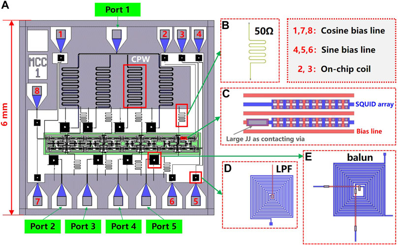
FIGURE 3. Layout design of MCC. (A) MCC overall layout. (B) Au strip functioned as 50 Ω impedance matching resistor. (C) Two sets of SQUID array where the Josephson junctions (JJ) are indicated by gray circles, and the bias lines run through along with these SQUID arrays. It is noticeable that, a large JJ of rectangular shape is utilized as contacting via of the bias lines on different layers. (D) A spiral inductor of about 15.6 nH acting as an LPF. (E) Balun for balancing the CPW and microstrip line.
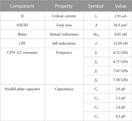
In order to share a common set of cosine and sine bias lines by the four isolators, a specific layout [27] has been adopted and modified for the design of MCC. The bias lines run through along with these SQUID arrays, as depicted in Figure 3C, where JJs are indicated by gray circles. It is notable that large rectangular JJs are utilized as contacting vias between different metal layers. To reduce the losses introduced by coupling the bias lines to the circuits, LPFs are inserted into the bias lines as they enter and exit the MCC, as exhibited in Figure 3D. Balun is an essential component for balancing between CPW and microstrip lines, as shown in Figure 3E. To prevent trapping flux vortices, a 5 μm width of the wiring lines is designed. Table 2 lists the parameters of various components of MCC, where the mutual inductance of baluns and the self-inductance of LPFs are calculated by InductEX @ software.
3 Fabrication process
The MCC is a relatively complicated multi-layer circuit which is completed in seven steps, including four-mask standard photolithography. Figure 4 shows the cross-sectional view of process flows and microscopic images of intermediate fabrication process of MCC, which includes SQUID, capacitor and normal metal.
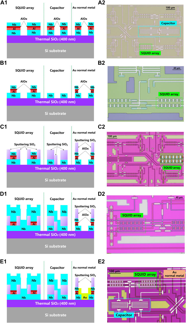
FIGURE 4. Cross-sectional view of process flows and microscopic image of intermediate fabrication process of MCC. (A1) Tri-layer Nb/Al-AlOx/Nb deposition and lift-off by using lithography mask #1. (B1) Junction definition by using lithography mask #2 and etching counter electrode Nb film with dry etching and Al-AlOx film with wet etching. (C1) RF sputtering deposition of SiO2 film and lift-off. (D1) DC sputtering deposition of the secondary Nb wiring layer and RIE etching by using lithography mask #3. (E1) Magnetron sputtering deposition of Au film and lift-off by using lithography mask #4. (A2–E2) The microscopic images of intermediate fabrication process corresponding to (A1–E1).
Step 1: A 4-inch double-sided polished Si (100) wafer is prepared. A 400 nm-thick SiO2 film is grown on both sides of the wafer by thermal oxidation.
Step 2: After the first lithography, the standard Nb/Al-AlOx/Nb tri-layer process [23,29] with thickness 150 nm/10 nm/150 nm is performed by DC magnetron sputtering method. The oxidization of Al is carried out in an O2 pressure of 400 mTorr at 20°C for about 5 h. This yields a critical current density of Jc ≈ 0.4 A/cm2 for the Josephson junctions. Then the primary base electrode pattern is accomplished by lift-off technology in Figure 4A1, where the layer stack-up of the tri-layer is displayed on the left column under the label of SQUID. The corresponding optical microscopic top view is displayed in Figure 4A2.
Step 3: As shown in Figure 4B1, by using reactive ion etching (RIE) with SF6 gas (60 mTorr and 200 sccm @ 30 W), the counter electrode Nb film is etched to define JJ after the second lithography. Wet etching is adopted for the Al-AlOx film with 80% phosphoric acid. This forms JJ and base electrode of capacitors. Figure 4B2 gives the corresponding optical microscopic top view, where the red dashed-line box indicates unfinished SQUID arrays.
Step 4: A 250 nm-thick SiO2 film is grown by RF magnetron sputtering as an isolation layer and the dielectric of capacitors. Lift-off technology is used to remove the unwanted SiO2, as illustrated in Figure 4C1. It is noticeable that, by removing the SiO2 layer above the counter electrodes of JJ, the contacting via-holes are constructed in a self-aligned manner [23,29]. Actually, large JJs are also utilized as contacting vias between different metal layers. Figure 4C2 shows the corresponding microscopic images and the inset is unfinished SQUID arrays with exposed counter electrodes (white circular dots).
Step 5: A 500 nm-thick Nb film is deposited by DC magnetron sputtering before a third lithography. Then the Nb film is etched by RIE, which can achieve wiring layer for connecting JJ in SQUID arrays, bias lines and the counter electrodes of capacitors, as exhibited in Figure 4D1. Figure 4D2 illustrates the corresponding optical microscopic top view, and the SQUID arrays are completed as shown in the yellow dashed-line box.
Step 6: A 225 μm-thick Au film is prepared by magnetron sputtering after the fourth photolithography, and the Au normal metal pattern is achieved by lift-off, as shown in Figures 4E1, E2.
Step 7: Finally, a 600 nm-thick Al film is prepared by DC magnetron sputtering on the back side of the wafer as ground plate for the microstrip line [23].
The entire fabrication process of MCC is accomplished and all steps are compatible with the semiconductor process. According to the microscope inspection, the success rate of MCC is about 88%. In this fabrication process, instead of using plasma enhanced chemical vapor deposition (PECVD) SiO2 film as the dielectric layer of capacitors [27,29], the sputtering SiO2 film is adopted both as isolation layer and dielectric layer of capacitors. As another key feature of the present process, large JJs are utilized as contacting vias between different metal layers. These process modifications are helpful to simplify the fabrication cycle in the initial research stage.
Figure 5A exhibits an optical micrograph of the completed MCC chip. The λ/2 CPW resonator is shown in Figure 5B. Detailed microphotographs of 50 Ω Au matching resistor is displayed in Figure 5C. Optical image and scanning electron microscope (SEM) image of SQUID arrays and bias lines are presented in Figures 5D, E, respectively.
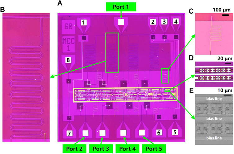
FIGURE 5. Microscopic image of MCC. (A) Optical image of chip. (B) λ/2 CPW resonator. (C) Au matching resistor of 50 Ω. (D) Two sets of SQUID array. (E) SEM image of SQUID arrays and bias lines.
4 Conclusion
In summary, this paper presents a design and fabrication process of a cryogenic MCC for the multiplexing XY control of superconducting quantum computers. With a frequency domain multiplexing ratio of 1:4 and designed working frequency between 4 and 8 GHz, the MCC is consisted of BPFs and isolators. The BPFs are implemented by λ/2 CPW resonators and the isolators are constructed by tunable inductor bridges based on SQUID arrays. The footprint of MCC is 6 × 6 mm2 which includes four λ/2 CPW resonators, 64 arrays of SQUIDs, eight capacitors, eight normal metal resistors, eight LPFs, eight baluns, a set of cosine bias line and sine bias line. Being compatible with semiconductor technology, the fabrication of MCC constitutes a set of four lithography masks and adopts self-aligned process of Josephson junctions. The on-chip cryogenic MCC could be integrated with the superconducting qubits on the same package at the base temperature stage (10 ∼ 30 mK) of a dilution refrigerator. The modular design of MCC could greatly reduce the number of microwave control lines and is hopeful to mitigate the interconnecting bottleneck problem towards the scaling-up of superconducting quantum computers.
Data availability statement
The original contributions presented in the study are included in the article/supplementary material, further inquiries can be directed to the corresponding authors.
Author contributions
Conceptualization, RH; methodology, RH; software, RH and YS; validation, RH and XG; formal analysis, RH and YS; writing—original draft preparation, RH; writing—review and editing, RH and LY; supervision, JL and WC; and project administration, JL and WC. All authors contributed to the article and approved the submitted version.
Funding
This work was supported by the key R&D program of Guangdong province (Grant No. 2019B010143002).
Acknowledgments
We gratefully acknowledge Weikai Xu, Jiaojiao Tian and Wanqi Xiong at Peking University, Changhao Zhao, Yongcheng He, Kaiyong He, Xinyu Wu, Qing Yu, Mingjun Cheng, Genting Dai, Guodong Chen, Yuxia Fu, Tao Zhong, Xiyou Li, Yalu Chen, Zhonghui Zhang, Li Zong, Bing Han, Changqing Yin, Liren Yan, Daoguang Liu and Xiaoming Wu for stimulating and valuable discussions.
Conflict of interest
The authors declare that the research was conducted in the absence of any commercial or financial relationships that could be construed as a potential conflict of interest.
Publisher’s note
All claims expressed in this article are solely those of the authors and do not necessarily represent those of their affiliated organizations, or those of the publisher, the editors and the reviewers. Any product that may be evaluated in this article, or claim that may be made by its manufacturer, is not guaranteed or endorsed by the publisher.
References
1. Blais A, Grimsmo AL, Girvin SM, Wallraff A. Circuit quantum electrodynamics. Rev Mod Phys (2021) 93:025005. doi:10.1103/revmodphys.93.025005
2. Bardin JC, Slichter DH, Reilly DJ. Microwaves in quantum computing. IEEE J microwaves (2021) 1:403–27. doi:10.1109/jmw.2020.3034071
3. Arute F, Arya K, Babbush R, Bacon D, Bardin JC, Barends R, et al. Quantum supremacy using a programmable superconducting processor. Nature (2019) 574:505–10. doi:10.1038/s41586-019-1666-5
4. Krantz P, Kjaergaard M, Yan F, Orlando TP, Gustavsson S, Oliver WD. A quantum engineer’s guide to superconducting qubits. Appl Phys Rev (2019) 6:021318. doi:10.1063/1.5089550
5. Bardin JC, Sank D, Naaman O, Jeffrey E. Quantum computing: an introduction for microwave engineers. IEEE Microwave Mag (2020) 21:24–44. doi:10.1109/mmm.2020.2993475
6. Ryu C, Samson E, Boshier MG. Quantum interference of currents in an atomtronic squid. Nat Commun (2020) 11:3338. doi:10.1038/s41467-020-17185-6
7. He K, Geng X, Huang R, Liu J, Chen W. Quantum computation and simulation with superconducting qubits. Chin Phys B (2021) 30:080304. doi:10.1088/1674-1056/ac16cf
8. He Y, Liu J, Zhao C, Huang R, Dai G, Chen W. Control system of superconducting quantum computers. J Superconductivity Novel Magnetism (2022) 35:11–31. doi:10.1007/s10948-021-06104-5
9. Gong M, Wang S, Zha C, Chen M-C, Huang H-L, Wu Y, et al. Quantum walks on a programmable two-dimensional 62-qubit superconducting processor. Science (2021) 372:948–52. doi:10.1126/science.abg7812
10. Jafferis D, Zlokapa A, Lykken JD, Kolchmeyer DK, Davis SI, Lauk N, et al. Traversable wormhole dynamics on a quantum processor. Nature (2022) 612:51–5. doi:10.1038/s41586-022-05424-3
11. Barends R, Kelly J, Megrant A, Veitia A, Sank D, Jeffrey E, et al. Superconducting quantum circuits at the surface code threshold for fault tolerance. Nature (2014) 508:500–3. doi:10.1038/nature13171
12. Kelly J, Barends R, Fowler AG, Megrant A, Jeffrey E, White TC, et al. State preservation by repetitive error detection in a superconducting quantum circuit. Nature (2015) 519:66–9. doi:10.1038/nature14270
13. White T, Opremcak A, Sterling G, Korotkov A, Sank D, Acharya R, et al. Readout of a quantum processor with high dynamic range josephson parametric amplifiers. Appl Phys Lett (2023) 122:014001. doi:10.1063/5.0127375
14. Rosenthal EI, Schneider CM, Malnou M, Zhao Z, Leditzky F, Chapman BJ, et al. Efficient and low-backaction quantum measurement using a chip-scale detector. Phys Rev Lett (2021) 126:090503. doi:10.1103/physrevlett.126.090503
15. Xue X, Patra B, van Dijk JP, Samkharadze N, Subramanian S, Corna A, et al. Cmos-based cryogenic control of silicon quantum circuits. Nature (2021) 593:205–10. doi:10.1038/s41586-021-03469-4
16. Bardin JC, Jeffrey E, Lucero E, Huang T, Das S, Sank DT, et al. Design and characterization of a 28-nm bulk-cmos cryogenic quantum controller dissipating less than 2 mw at 3 k. IEEE J Solid-State Circuits (2019) 54:3043–60. doi:10.1109/JSSC.2019.2937234
17. Patra B, Incandela RM, Van Dijk JP, Homulle HA, Song L, Shahmohammadi M, et al. Cryo-cmos circuits and systems for quantum computing applications. IEEE J Solid-State Circuits (2017) 53:309–21. doi:10.1109/jssc.2017.2737549
18. Pauka S, Das K, Kalra R, Moini A, Yang Y, Trainer M, et al. A cryogenic cmos chip for generating control signals for multiple qubits. Nat Electro (2021) 4:64–70. doi:10.1038/s41928-020-00528-y
19. Lecocq F, Quinlan F, Cicak K, Aumentado J, Diddams S, Teufel J. Control and readout of a superconducting qubit using a photonic link. Nature (2021) 591:575–9. doi:10.1038/s41586-021-03268-x
20. McDermott R, Vavilov M, Plourde B, Wilhelm F, Liebermann P, Mukhanov O, et al. Quantum–classical interface based on single flux quantum digital logic. Quan Sci Technol (2018) 3:024004. doi:10.1088/2058-9565/aaa3a0
21. McDermott R, Vavilov M. Accurate qubit control with single flux quantum pulses. Phys Rev Appl (2014) 2:014007. doi:10.1103/physrevapplied.2.014007
22. Huang R, Geng X, Wu X, Dai G, Yang L, Liu J, et al. Cryogenic multiplexing control chip for a superconducting quantum processor. Phys Rev Appl (2022) 18:064046. doi:10.1103/physrevapplied.18.064046
23. Huang R, Geng X, Dai G, Yang L, Liu J, Chen W. Design and fabrication of integrated superconducting isolator-circulator-isolator chip. Microelectronic Eng (2022) 263:111844. doi:10.1016/j.mee.2022.111844
24. Kerckhoff J, Lalumière K, Chapman BJ, Blais A, Lehnert K. On-chip superconducting microwave circulator from synthetic rotation. Phys Rev Appl (2015) 4:034002. doi:10.1103/physrevapplied.4.034002
25. Rosenthal EI, Chapman BJ, Higginbotham AP, Kerckhoff J, Lehnert K. Breaking lorentz reciprocity with frequency conversion and delay. Phys Rev Lett (2017) 119:147703. doi:10.1103/physrevlett.119.147703
26. Chapman BJ, Rosenthal EI, Lehnert K. Design of an on-chip superconducting microwave circulator with octave bandwidth. Phys Rev Appl (2019) 11:044048. doi:10.1103/physrevapplied.11.044048
27. Chapman BJ, Rosenthal EI, Kerckhoff J, Moores BA, Vale LR, Mates J, et al. Widely tunable on-chip microwave circulator for superconducting quantum circuits. Phys Rev X (2017) 7:041043. doi:10.1103/physrevx.7.041043
28. Chapman BJ, Moores BA, Rosenthal EI, Kerckhoff J, Lehnert K. General purpose multiplexing device for cryogenic microwave systems. Appl Phys Lett (2016) 108:222602. doi:10.1063/1.4952772
Keywords: multiplexing control, non-reciprocity, superconducting quantum computer, fabrication, SQUID
Citation: Huang R, Shi Y, Geng X, Yang L, Liu J and Chen W (2023) Design and fabrication of cryogenic multiplexing control chip. Front. Phys. 11:1212642. doi: 10.3389/fphy.2023.1212642
Received: 26 April 2023; Accepted: 30 October 2023;
Published: 09 November 2023.
Edited by:
Weilong Wang, State Key Laboratory of Mathematical Engineering and Advanced Computing, ChinaCopyright © 2023 Huang, Shi, Geng, Yang, Liu and Chen. This is an open-access article distributed under the terms of the Creative Commons Attribution License (CC BY). The use, distribution or reproduction in other forums is permitted, provided the original author(s) and the copyright owner(s) are credited and that the original publication in this journal is cited, in accordance with accepted academic practice. No use, distribution or reproduction is permitted which does not comply with these terms.
*Correspondence: Rutian Huang, aHJ0MTdAdHNpbmdodWEub3JnLmNu; Wei Chen, d2VpY2hlbkB0c2luZ2h1YS5lZHUuY24=
 Rutian Huang
 Yunfan Shi1,2
 Xiao Geng