 Kun Yue†
 Xialian Feng
 Jiaxin Yu
- Laboratory of Integrated Opto-Mechanics and Electronics, Shanghai Key Laboratory of Modern Optical System, School of Optical-Electrical and Computer Engineering, University of Shanghai for Science and Technology, Shanghai, China
Confining light at a subwavelength scale is important for building ultracompact opto-electronic networks. Plasmonic waveguides are good candidate devices for this purpose. However, the oscillation of electrons relating to surface plasmon polaritons causes energy dissipation, which limits the propagation length and thus reduces the waveguide performance. Here, we design a low-loss plasmonic waveguide composed of a nanowire dimer structure on a metal substrate, in which the dominant modes are localized within the air gap between the nanowires and referred to as air-host plasmonic modes. The use of air instead of dielectric materials as the host medium can reduce ohmic loss and avoid the dispersion effect of dielectric. When the constructed nanowires have a diameter less than 100 nm, the air-host mode has subwavelength-scale confinement and a propagation length of ∼100 μm, which has broad application prospects for the construction of ultracompact plasmonic devices.
1 Introduction
Plasmonic waveguides can support surface plasmon polaritons (SPPs) with a volume breaking through the optical diffraction limit [1, 2]. The strong field confinement of SPPs can enhance the interaction between light and materials [3, 4], which is beneficial for constructing energy-saving devices. Furthermore, plasmonic waveguides are small compared with traditional optical waveguides [5, 6]. Both features promise the development of ultracompact opto-electronic networks [7–11]. However, with free electrons collectively oscillating on the interface of the medium and metal, plasmonic modes suffer ohmic losses, and the energy dissipation reduces the performance of constructed devices. A figure of merit of plasmonic waveguides is a reduced ohmic loss while the field confinement of SPPs is sustained [12]. As the ohmic loss positively correlates with the dielectric index, a typical design is to insert a low-index gap layer (e.g., a MgF2 or SiO2 layer) between the high-index gain medium (e.g., a semiconductor nanowire) and the metal substrate (Figure 1A). The plasmonic mode then propagates along the dielectric-metal interface (in what is referred to as the dielectric-host mode) with far less loss [5, 13]. The ohmic loss can be further reduced using a medium having a lower refractive index, such as air [14], but simply replacing the dielectric with air is unfeasible as the active medium is not physically supported. Here, we design a nanowire dimer plasmonic waveguide by placing two semiconductor nanowires on a metal substrate (Figure 1B). By optimising parameters of the structure (i.e., the diameter and separation of the nanowires and the thickness of the dielectric layer), a low-loss propagating mode is supported in the air gap within the dimer (referred to as the air-host mode), resulting in a propagation length comparable to that of traditional single-nanowire waveguides but stronger mode confinement. Moreover, the modal field is concentrated in the air gap and is maximum at the air–dielectric interface, and the structure can thus be integrated with a microfluid chip for lasing or sensing [15]. This structure has wide prospects as a versatile platform for high-density optoelectronic devices.
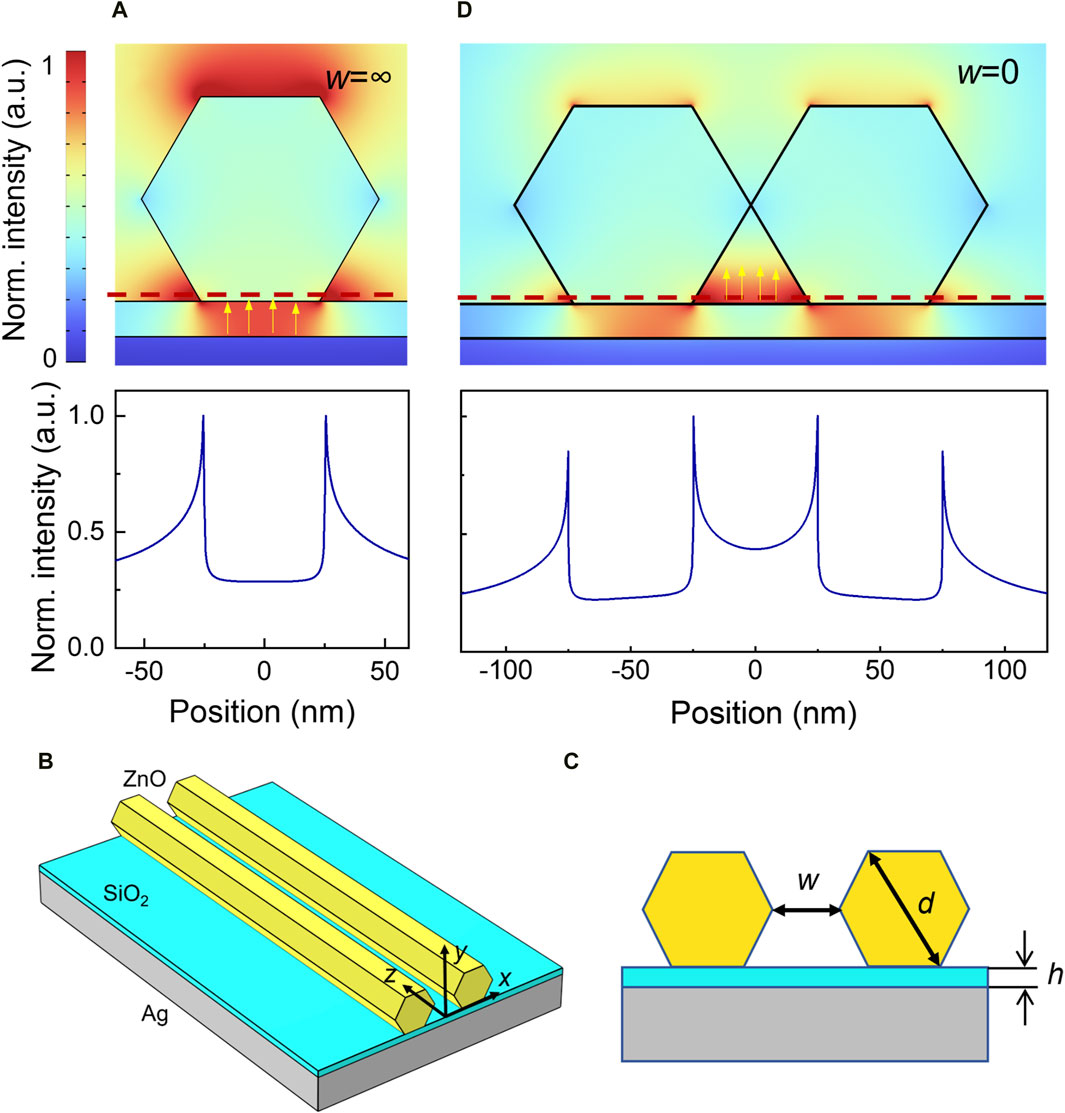
Figure 1. Nanowire dimer plasmonic waveguide. (A) Electrical field distribution of a traditional single-nanowire plasmonic waveguide, which is extracted from the resonance at around 747 nm. Three-dimensional (B) and cross-section (C) of a nanowire dimer structure. d denotes the diameter of the nanowire, w denotes the distance between two nanowires, and h denotes the thickness of the dielectric layer (SiO2). (D) Field distribution of a nanowire dimer. The corresponding electric fields in (A,D) are extracted at 0.1 nm above the air–SiO2 interface with d = 100 nm. The arrows in (A,D) show the orientation of the electric field.
2 Methods
Figure 1C presents the cross-section of a nanowire dimer plasmonic waveguide with its key parameters. The two nanowires are made from hexagonal wurtzite-structured ZnO and have a separation w, and the metal substrate is a SiO2 dielectric layer (with thickness h) deposited on bulk Ag. A simulation is performed adopting finite-difference time-domain methods for mode analysis.
3 Results and discussion
The two ZnO nanowires form an air gap between themselves and the substrate (i.e., between their feet) as illustrated in Figure 1D. For a single-nanowire waveguide (lower panel in Figure 1A), except for the strong electric field preserved in the dielectric-host mode [5, 16], there is a non-negligible field outside the nanowire. It indicates a poor light confinement especially in the case of small d (e.g., 100 nm). When two nanowires are close to one another, the fields at the enclosed foot points couple into a hybrid mode propagating in the air gap (i.e., the air-host mode), and the hybrid mode outcompetes the dielectric-host mode and dominates the propagation at small d (Figure 1D). This air-host mode has field vectors perpendicular to the substrate, and the intensity of the electric field decays evanescently with distance along the direction normal to the interface, indicating its plasmonic mode nature [12].
Inserting a dielectric layer between the metal substrate and nanowires further reduces the ohmic loss and enhances the electric field in the subwavelength local range. Therefore, we first investigate the influence of the dielectric layer on the mode fields. Figure 2A plots the distribution of mode fields along the air–SiO2 interface (y = 0.1 nm) for different d. Compared with the structure without a SiO2 layer (i.e., h = 0), the structure with a 5-nm-thick layer has a much stronger electric field for the air-host mode. However, in contrast with a dielectric-host mode, which is highly sensitive to h [5, 17], the air-host mode is almost unaffected by the thickness of h unless it exceeds the penetration length of the SPPs (e.g., h > 50 nm). The lower dependence on h is beneficial to future applications due to the better tolerance of device processing. Figure 2B shows the electric field along x = 0 for nanowire dimer waveguides without (I) and with a 15-nm thick dielectric layer (II). The air-host modes of the two structures have a plasmonic feature as the intensity of the electric field decreases from the bottom of the air gap. However, for the waveguide with a SiO2 layer, the electric field in the air gap is much stronger than that in the SiO2 layer, confirming the lower loss in air. The air-host modes can exist across a wide wavelength range, for example, from 620 nm to 1,032 nm for a dimer structure with d = 100 nm, w = 0, and h = 15 nm. Apart from hexagonal crystals, dimer structures composed of nanowires with other crystal types (as tetragonal crystals) also support such air-host modes. In contrast with the mode field confined in the solid dielectric layer of a traditional single-nanowire waveguide (Figure 2C), having a field confined in air makes the waveguide easier to functionalise and modulate for applications.
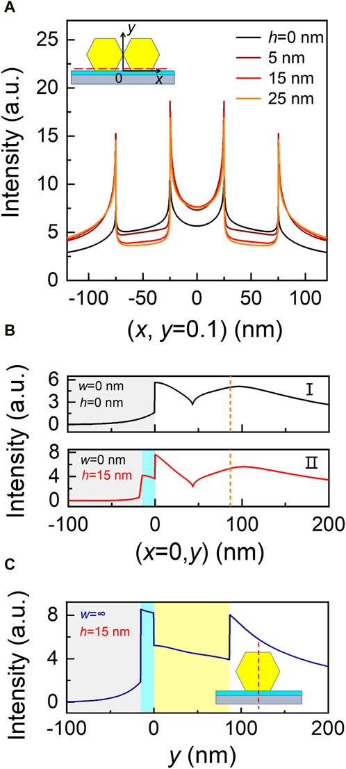
Figure 2. Dependence of the air-host mode on the thickness of the dielectric layer. (A) Dependence of the electric field at y = 0.1 nm (where y = 0 is set as the air−SiO2 interface) on the layer thickness h (w = 0, d = 100 nm). When there is no dielectric layer (h = 0), the air-host mode is at its weakest, with an electric field comparable to the field within the nanowires, indicating a large ohmic loss from the metal substrate. An extra dielectric layer (h ≠ 0) helps to suppress the loss to the mode field, but there is little difference in the loss as h increases from 5 to 25 nm. The independence of the air-host mode on h implies high tolerance to processing. (B) Dependence of the electric field at x = 0 (in the middle of the air gap) on the dielectric layer. The areas shaded grey and cyan are the metal and SiO2 dielectric areas, respectively. The dashed lines indicate the top edges of the semiconductor nanowires. The intensity is maximal at the air−X interface (where X denotes metal for h = 0 or SiO2 for h ≠ 0) both with and without a SiO2 layer, allowing coupling with active media settled in the air gap. (C) Field distribution of the dielectric-host mode at the middle of a single-nanowire plasmonic waveguide (d = 100 nm and h = 15 nm). The field is maximal at the metal−SiO2 interface, which is comparable to the situation in (B).
To gain a deeper understanding of the air-host mode, we analyse the dependence of the effective refractive index (neff) on d and h, where
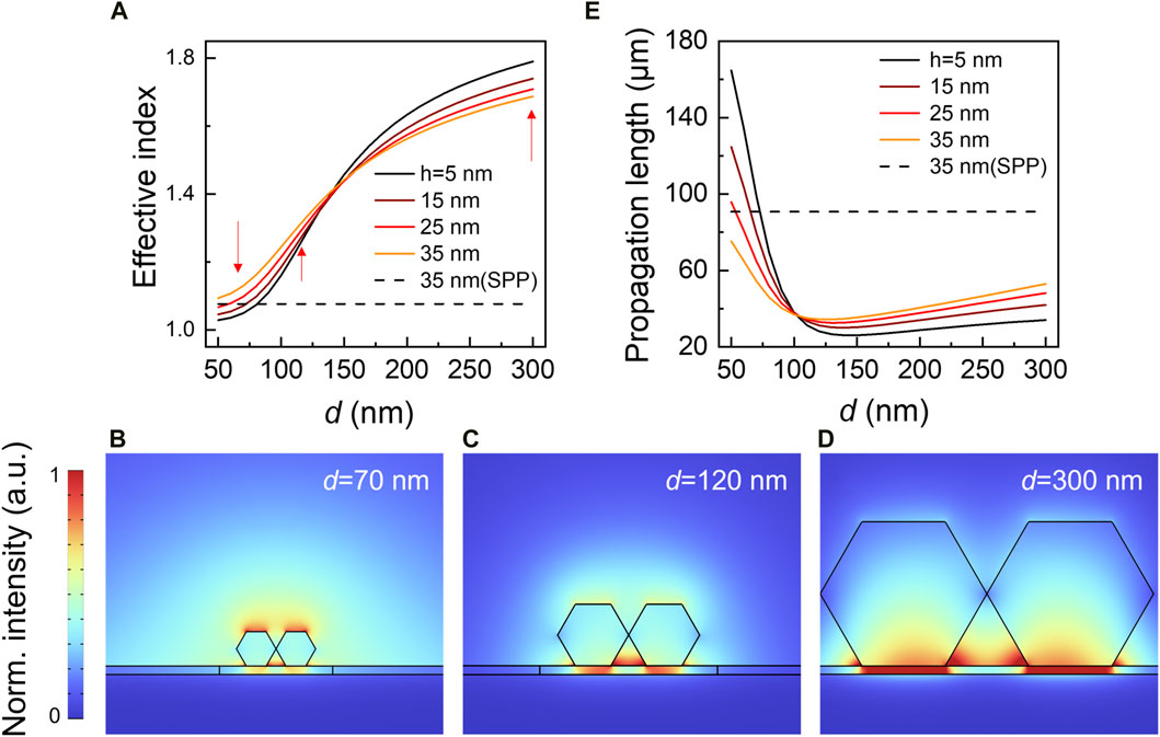
Figure 3. Evolution from the air-host mode to the dielectric-host mode through changes in d and h: dependence of the mode effective refractive index (A) and propagation length (E) on d and h. The dashed line provides data for SPPs supported on bare substrates without nanowires. Both the effective index and propagation length depend strongly on d but only slightly on h. (B–D) Electric field diagrams for d = 70, 120, and 300 nm (h = 15 nm, w = 0 nm), showing the evolution of dominance from the air-host mode to dielectric-host mode.
The ohmic losses corresponding to the two modes are quantified by the imaginary part of the effective index, Im{neff}, which further determines the propagation length (LP). LP can be calculated by
Light−matter interactions are of great interest owing to their potential applications in such as lasing and sensing [21, 22]. The basic idea of using an optical waveguide to enhance such interaction is to confine light in a small spatial region and to increase the light−matter overlap. The confinement can be quantified by the effective mode area (Aeff) [13], expressed as
Here, the energy density W(r) is defined as
where ω is the mode resonance frequency, ε(r) is the complex relative permittivity, and μ0 is the vacuum permeability. Aeff calculated from Eqs (1, 2) is then normalised by the square of the wavelength (i.e., we take
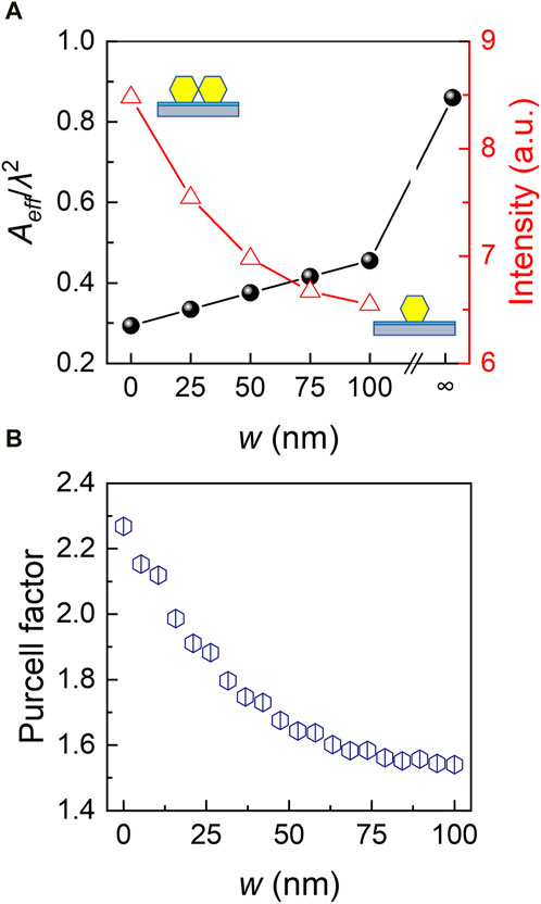
Figure 4. Mode confinement and Purcell effect of a nanowire-dimer waveguide. (A) Variations in the normalised effective mode area and electric field intensity with w. The electric field intensity is extracted from the central axis of the air gap, 0.1 nm above the air–SiO2 interface. The nanowire-dimer waveguide with w = 0 has the most confined field, the intensity of which is only 1/3 of that of a single-nanowire waveguide (w = ∞). (B) Variation in the Purcell factor with w. The strongest enhancement of spontaneous emission is achieved using a nanowire-dimer waveguide with w = 0.
As the maximum field appears in the air gap (namely, at the air−SiO2 interface) rather than in a bulk medium, an optimal light−matter interaction can be easily achieved by placing active materials at the interface [21, 24], which is meaningful for applications. For example, by attaching a monolayer semiconductor (such as transition metal chalcogenides) at the interface, a perfect overlap between the two-dimensional gain medium and mode is achieved. The modal gain is thus maximised for plasmonic lasing [22, 25]. The waveguide modification of the spontaneous emission can be quantified using the Purcell factor (FP) [26]. The spontaneous emission of excitons in the monolayers (∼1.0 nm in thickness) is mimicked by setting electric dipole sources in the middle of the air gap and 0.1 nm above the interface, and the enhancement of the recombination rate can be simulated by the change in the lifetime. As shown in Figure 4B, FP increases as the nanowire coupling strengthens and has a maximal value of 2.3 at w = 0. As the intensity at the foot points can be even stronger, the actual FP can be even higher. Due to the strong mode confinement and Purcell effect, the nanowire dimer structure has good potential for ultracompact plasmonic active devices using atomically thick active media [27, 28].
4 Conclusion
In summary, we proposed a plasmonic waveguide composed of a nanowire dimer on a metal substrate. The air-host mode supported by such a nanowire dimer structure has low ohmic loss and thus a long propagation length. Compared with a single nanowire plasmonic waveguide, the nanowire dimer waveguide has stronger mode confinement, a high Purcell factor at the air−dielectric interface, and thus more intense light−matter interaction. In addition, the properties of the waveguides have higher tolerance to the processing of the dielectric layer. As the dominant mode of propagation is in an air gap instead of a dielectric solid, nanowire dimer plasmonic waveguides are a more versatile platform for constructing functional integrated devices.
Data availability statement
The original contributions presented in the study are included in the article, further inquiries can be directed to the corresponding author.
Author contributions
KY: Formal Analysis, Investigation, Writing–original draft. XF: Formal Analysis, Investigation, Writing–review and editing. JY: Conceptualization, Funding acquisition, Supervision, Writing–original draft, Writing–review and editing. FG: Funding acquisition, Writing–review and editing.
Funding
The author(s) declare that financial support was received for the research, authorship, and/or publication of this article. This work was supported by the National Natural Science Foundation of China (NSFC) (Grant Nos 12074259, 62075131, and 62122054).
Conflict of interest
The authors declare that the research was conducted in the absence of any commercial or financial relationships that could be construed as a potential conflict of interest.
Publisher’s note
All claims expressed in this article are solely those of the authors and do not necessarily represent those of their affiliated organizations, or those of the publisher, the editors and the reviewers. Any product that may be evaluated in this article, or claim that may be made by its manufacturer, is not guaranteed or endorsed by the publisher.
References
1. Zhu W, Xu T, Wang H, Zhang C, Deotare PB, Agrawal A, et al. Surface plasmon polariton laser based on a metallic trench Fabry-Perot resonator. Sci Adv (2017) 3:e1700909. doi:10.1126/sciadv.1700909
2. Zhang Q, Li G, Liu X, Qian F, Li Y, Sum TC, et al. A room temperature low-threshold ultraviolet plasmonic nanolaser. Nat Commun (2014) 5:4953. doi:10.1038/ncomms5953
3. Ning CZ. Semiconductor nanolasers and the size-energy-efficiency challenge: a review. Adv Photon (2019) 1:1. doi:10.1117/1.AP.1.1.014002
4. Ma RM, Oulton RF, Sorger VJ, Bartal G, Zhang X. Room-temperature sub-diffraction-limited plasmon laser by total internal reflection. Nat Mater (2011) 10:110–3. doi:10.1038/nmat2919
5. Oulton RF, Sorger VJ, Zentgraf T, Ma RM, Gladden C, Dai L, et al. Plasmon lasers at deep subwavelength scale. Nature (2009) 461:629–32. doi:10.1038/nature08364
6. Tao T, Zhi T, Liu B, Dai J, Zhuang Z, Xie Z, et al. Manipulable and hybridized, ultralow-threshold lasing in a plasmonic laser using elliptical inGaN/GaN nanorods. Adv Funct Mater (2017) 27:1703198. doi:10.1002/adfm.201703198
7. Noginov MA, Zhu G, Belgrave AM, Bakker R, Shalaev VM, Narimanov EE, et al. Demonstration of a spaser-based nanolaser. Nature (2009) 460:1110–2. doi:10.1038/nature08318
8. Toanen V, Symonds C, Benoit JM, Gassenq A, Lemaitre A, Bellessa J. Room-Temperature lasing in a low-loss tamm plasmon cavity. ACS Photon (2020) 7:2952–7. doi:10.1021/acsphotonics.0c00781
9. Suh JY, Kim CH, Zhou W, Huntington MD, Co DT, Wasielewski MR, et al. Plasmonic bowtie nanolaser arrays. Nano Lett (2012) 12:5769–74. doi:10.1021/nl303086r
10. Liu Y, Ma Y. One-dimensional plasmonic sensors. Front Phys (2020) 8:312. doi:10.3389/fphy.2020.00312
11. Linghu S, Gu Z, Lu J, Fang W, Yang Z, Yu H, et al. Plasmon-driven nanowire actuators for on-chip manipulation. Nat Commun (2021) 12:385. doi:10.1038/s41467-020-20683-2
12. De Leon I, Berini P. Amplification of long-range surface plasmons by a dipolar gain medium. Nat Photon (2010) 4:382–7. doi:10.1038/nphoton.2010.37
13. Wang Y, Wang S, Cai M, Liu H. A long propagation distance hybrid triangular prism waveguide for ultradeep subwavelength confinement. IEEE Sens J (2019) 19:11159–66. doi:10.1109/JSEN.2019.2935750
14. Hentschel M, Koshelev K, Sterl F, Both S, Karst J, Shamsafar L, et al. Dielectric Mie voids: confining light in air. Light Sci Appl (2023) 12:3. doi:10.1038/s41377-022-01015-z
15. Anker JN, Hall WP, Lyandres O, Shah NC, Zhao J, Van Duyne RP. Biosensing with plasmonic nanosensors. Nat Mater (2008) 7:442–53. doi:10.1038/nmat2162
16. Liu X, Zhang Q, Yip JN, Xiong Q, Sum TC. Wavelength tunable single nanowire lasers based on surface plasmon polariton enhanced Burstein-Moss effect. Nano Lett (2013) 13:5336–43. doi:10.1021/nl402836x
17. Li Z, Bao K, Fang Y, Guan Z, Halas NJ, Nordlander P, et al. Effect of a proximal substrate on plasmon propagation in silver nanowires. Phys Rev B Condens Matter Mater Phys (2010) 82:241402. doi:10.1103/PhysRevB.82.241402
18. Wuestner S, Hamm JM, Pusch A, Hess O. Plasmonic leaky-mode lasing in active semiconductor nanowires. Laser Photon Rev (2015) 9:256–62. doi:10.1002/lpor.201400231
19. Chen Y, Gregersen N, Nielsen TR, Mørk J, Lodahl P. Spontaneous decay of a single quantum dot coupled to a metallic slot waveguide in the presence of leaky plasmonic modes. Opt Express (2010) 18:12489–98. doi:10.1364/oe.18.012489
20. Bian Y, Gong Q. Tuning the hybridization of plasmonic and coupled dielectric nanowire modes for high-performance optical waveguiding at sub-diffraction-limited scale. Sci Rep (2014) 4:6617. doi:10.1038/srep06617
21. De Torres J, Ferrand P, Colas Des Francs G, Wenger J. Coupling emitters and silver nanowires to achieve long-range plasmon-mediated fluorescence energy transfer. ACS Nano (2016) 10:3968–76. doi:10.1021/acsnano.6b00287
22. Liu X, Galfsky T, Sun Z, Xia F, Lin EC, Lee YH, et al. Strong light-matter coupling in two-dimensional atomic crystals. Nat Photon (2014) 9:30–4. doi:10.1038/nphoton.2014.304
23. Oulton RF, Sorger VJ, Genov DA, Pile DFP, Zhang X. A hybrid plasmonic waveguide for subwavelength confinement and long-range propagation. Nat Photon (2008) 2:496–500. doi:10.1038/nphoton.2008.131
24. Sidiropoulos TPH, Röder R, Geburt S, Hess O, Maier SA, Ronning C, et al. Ultrafast plasmonic nanowire lasers near the surface plasmon frequency. Nat Phys (2014) 10:870–6. doi:10.1038/nphys3103
25. Paik EY, Zhang L, Burg GW, Gogna R, Tutuc E, Deng H. Interlayer exciton laser of extended spatial coherence in atomically thin heterostructures. Nature (2019) 576:80–4. doi:10.1038/s41586-019-1779-x
26. Barthes J, Colas DFG, Bouhelier A, Weeber JC, Dereux A. Purcell factor for a point-like dipolar emitter coupled to a two-dimensional plasmonic waveguide. Phys Rev B Condens Matter Mater Phys (2011) 84:073403. doi:10.1103/PhysRevB.84.073403
27. Liao F, Yu J, Gu Z, Yang Z, Hasan T, Linghu S, et al. Enhancing monolayer photoluminescence on optical micro/nanofibers for low-threshold lasing. Sci Adv (2019) 5:eaax7398. doi:10.1126/sciadv.aax7398
Keywords: plasmonic waveguide, nanowire dimer, ohmic loss reduction, light confinement, airhost plasmonic mode
Citation: Yue K, Feng X, Yu J and Gu F (2024) Long-range air-host plasmonic propagation with subwavelength confinement. Front. Phys. 12:1386585. doi: 10.3389/fphy.2024.1386585
Received: 15 February 2024; Accepted: 20 March 2024;
Published: 05 April 2024.
Edited by:
Xiao Lin, Zhejiang University, ChinaCopyright © 2024 Yue, Feng, Yu and Gu. This is an open-access article distributed under the terms of the Creative Commons Attribution License (CC BY). The use, distribution or reproduction in other forums is permitted, provided the original author(s) and the copyright owner(s) are credited and that the original publication in this journal is cited, in accordance with accepted academic practice. No use, distribution or reproduction is permitted which does not comply with these terms.
*Correspondence: Jiaxin Yu, eXVqaWF4aW5AdXNzdC5lZHUuY24=
†These authors have contributed equally to this work