 Katharine Snow
 Fatemeh Moradiani
 Hamidreza Siampour
- School of Mathematics and Physics, Queen’s University Belfast, University Road, Belfast, United Kingdom
We report on the design and simulation of strip-loaded nanophotonic interfaces aimed at improving resonant coupling and photon routing efficiency. In our design, the guided mode is confined within a plane by a high-index thin film and is loosely confined laterally by a lower index strip. Using a hydrogen silsesquioxane (HSQ) strip, titanium dioxide core, and silicon dioxide substrate, we optimise the waveguide dimensions for maximum lateral confinement of light. Specifically, we propose a polymer-based Bragg grating cavity and ring resonator that achieve near-optimal mode volumes and high Q-factors. These may be further developed to achieve the even higher Q-factors demanded by quantum technologies. Our calculations suggest that a quantum dot embedded in a cavity with a mode volume of
Introduction
Quantum emitters of single indistinguishable photons are critical for advancing quantum technologies such as computing [1], networking [2], cryptography [3], and metrology [4]. Currently, spontaneous parametric down-conversion is the prevalent method for single-photon generation, but its probabilistic nature limits how far the efficiency and indistinguishability of photons can be simultaneously increased [5]. Solid-state emitters, including semiconductor quantum dots [6, 7] and diamond colour centres [8, 9], offer promising alternatives that are not subject to the same constraints when integrated with nanophotonic devices. By placing the emitters inside a high-Q cavity, the emitter’s decay rate is enhanced by the Purcell factor
To achieve narrowband enhancement of the zero-phonon line (ZPL), the cavity decay rate
where
Micropillar cavities are chosen for their high
Here, we propose a polymer-based Bragg grating cavity and ring resonator. Such polymer-based nanophotonic devices can be fabricated with very high precision using current fabrication technology [9, 19]. Due to the low refractive index of hydrogen silsesquioxane (HSQ) polymer, we choose a strip-loaded waveguide geometry, which results in a larger mode volume than current devices, with
Results and discussion
Bragg grating cavity
In a strip-loaded waveguide, the mode is confined within a plane by a high-index thin film and is loosely confined in the lateral direction by a lower index strip, as shown in Figure 1Ai. We choose an HSQ strip, titanium dioxide core, and silicon dioxide substrate, and optimise the waveguide dimensions for maximum lateral confinement of light with a vacuum wavelength of approximately 600 nm. The optimal dimensions are as follows: strip height of 180 nm, strip width of 300 nm, and core thickness of 70 nm. A Bragg cavity is constructed based on this waveguide geometry, with the Bragg reflectors being twice as long as the waveguide is wide, as shown in the inset of Figure 1Aii. The transmission spectrum of this cavity is shown in Figure 1Aii for different values of the total number of Bragg reflectors N. For N = 100, the quality factor is found to be 230 and the outcoupling efficiency, defined as the cavity-waveguide coupling ratio, is 90%. The cavity mode is shown in Figure 1C, and the mode volume is found to be 6.96
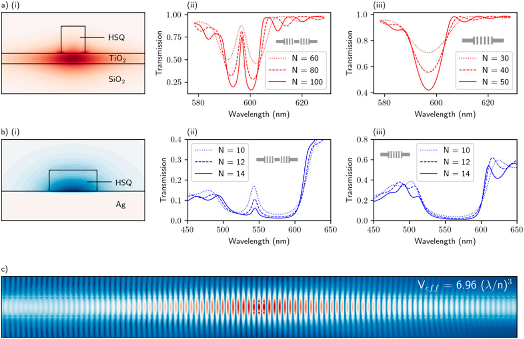
Figure 1. Electromagnetic simulations of polymer-based nanophotonic devices. (A) A strip-loaded waveguide and (B) a plasmonic waveguide. Cross-sections of the modes are depicted in (i). Transmission spectra for the corresponding Bragg cavities and Bragg reflectors are presented in (ii) and (iii), respectively, for various values of N, the number of reflectors. The strip-loaded cavity mode for N = 100 is shown in (C).
The quantum emitter should be embedded in the cavity at the position where the cavity mode electric field is maximal. Emitted photons need to have both high indistinguishability, defined as the ability of two photons to interfere on a beam-splitter in a Hong-Ou-Mandel setup, and high quantum efficiency, defined as the fraction of photons emitted into the cavity. In the narrowband-enhancement weak-coupling regime (see Figure 2), the indistinguishability and efficiency of emitted photons are given by
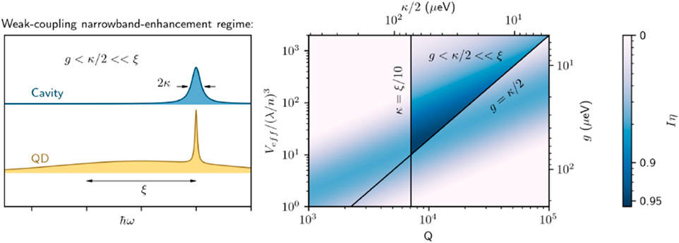
Figure 2. The narrowband-enhancement weak-coupling regime for a quantum dot embedded in a nanophotonic cavity. Left: A sketch illustrating the different energy scales of importance, where the cavity linewidth is much smaller than the typical energy scale of phonons. Right: The product
To determine the indistinguishability, we follow ref. [10]: we assume that the dominant contribution to the dephasing
where
Directional coupler
The concept of the directional coupler, introduced in the mid-20th century, has been foundational for many advancements in optical and microwave technologies [24]. While the fundamental idea remains relevant, the design of the entire structure—including S-bends and a chain of materials tailored for specific applications—continues to hold significant importance in contemporary engineering. More recently, the directional coupler has become a crucial component in photonic quantum integrated circuits, demonstrating the capability to facilitate quantum computing logic operations when employed with single photons [25–27].
In this section, we present two platforms for directional couplers: one based on dielectric-loaded surface plasmon polariton (DLSPP) waveguides and the other on strip-loaded waveguide configurations. We then compare the two structures in terms of their applicability for single-photon routing. Notably, the overall dimensions of both platforms are consistent with the Bragg grating cavity structure discussed in the previous section.
The directional coupler is designed for both parallel straight waveguides and S-bends based on sine curves, enabling continuous bend curvature and adiabatic modification [28–30] of the DLSPP waveguide and the strip-loaded waveguide mode throughout the bend, as shown in Figures 3Ai, Bi, respectively. One crucial aspect to consider is the design of the S-bend. As illustrated in Figure 3A, the losses associated with the S-bend can be categorised into transition losses and radial losses.
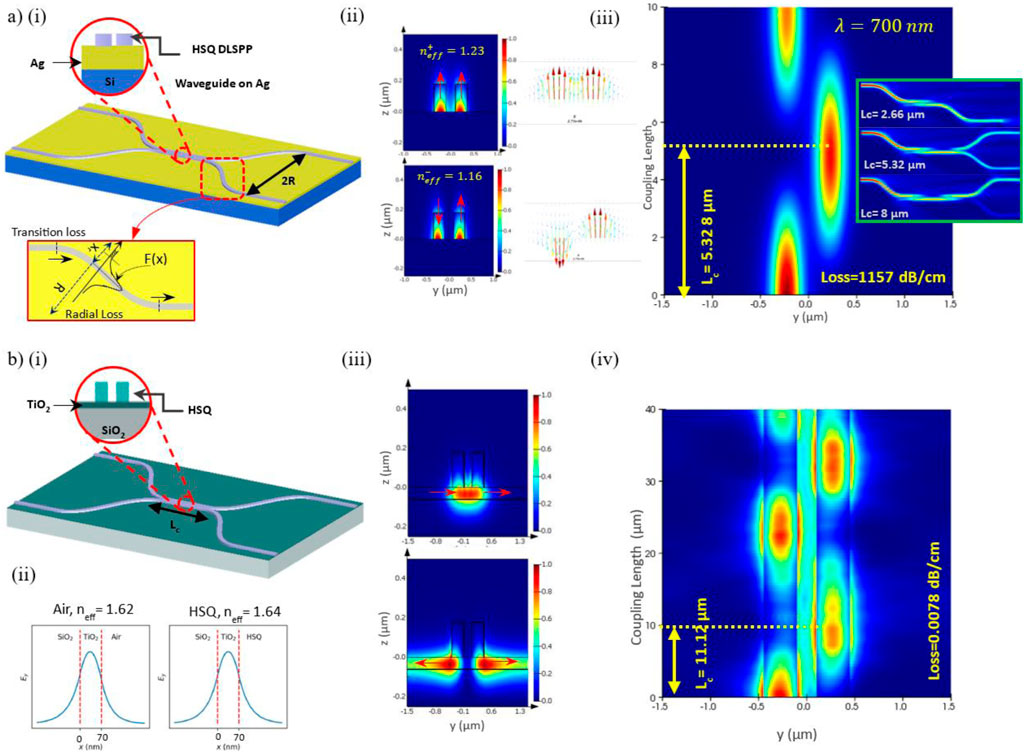
Figure 3. (A) Simulation results of a DLSPP-based directional coupler structure consisting of two rectangular DLSPP waveguides with a height of h = 180 nm, width of w = 250 nm, refractive index nd = 1.41, a separation gap of g = 200 nm in the parallel section, and an S-bend waveguide with a 2.5 µm radius. The length of the parallel section (coupling length) is Lc = 5.3 µm, designed to impart a π phase shift and achieve 50–50 power splitting at λ = 700 nm between the (ii) symmetric (
Radial losses occur due to the limited guiding of the propagation mode caused by speed limitations beyond the outer end of the bent waveguide. Transition losses occur when there are discontinuities in the curvature of the waveguide, where sudden changes in modal propagation characteristics take place. The guided modes in curved waveguides are broader compared to straight waveguides and change outward along the curve. The normalised transition loss due to mismatch between the straight waveguide mode and the curvature can be calculated as follows in Equation 3 [29].
where
In this study, we utilised the commercial software Lumerical FDTD to calculate the minimum bending radius Rmin. The design of the S-bends was based on sine curves [31, 32], allowing for continuous bend curvature and thereby adiabatic modification of the mode throughout the bend. For the DLSPP structure, due to its high optical contrast and strong confinement of the DLSPP mode, a curvature radius as small as 2 μm still transmitted a significant portion of the DLSPP mode (>50%). This finding is consistent with experimental measurements using scanning near-field optical microscopy (SNOM) [31].
For the strip-loaded structure, where the effective mode index with HSQ cladding differs from that with air by a small amount of 0.02 (from 1.64 to 1.62, as shown in Figure 3Bii), the minimum bending radius must be sufficiently large to allow the light to bend effectively. We calculated this value from simulations to be 100 µm [33], which is close to the value obtained from the analytical expression in reference [34]. From this expression,
This characteristic is crucial for designing optical devices with tight bends and for sensitive optical applications, such as single-photon routing. However, in applications like single-photon sources, the overall propagation length is limited by structural and environmental factors when the emitter is coupled to the waveguide. Although the photon propagation length is generally longer than that of SPPs, issues may arise concerning the structure’s overall length. Additionally, in these structures, distinguishability may be significantly compromised at very high dimensions. Nevertheless, the strip-loaded structure remains a strong option for applications where minimising loss is the primary concern.
The interaction length required to achieve the desired power coupling to the second waveguide is calculated using
Ring resonator
Another approach to enhancing the Purcell effect is to use DLSPP waveguide-ring resonators (WRRs). A WRR, consisting of a straight waveguide laterally coupled to a ring resonator, typically provides more pronounced wavelength selection and a high
Figure 4A shows a 3D schematic of the DLSSP-WRR structure, designed with the same parameters discussed in the previous section. Figure 4B presents the transmission spectrum for a ring with a radius of 2.5 µm and three different separations (g) of 200 nm, 150 nm, and 100 nm. A 100 nm gap provides a higher extinction ratio compared to the other gaps, though this enhanced coupling efficiency also leads to mode broadening. Figure 4C depicts the full profile of the structure at a resonant wavelength of 616.4 nm and a non-resonant wavelength of 623 nm. The bandwidth of the WRR is determined by the radius of the ring resonator and the wavelength-dependent effective index of the bent waveguide. Figure 4D displays the transmission spectra for a 100 nm separation and ring radii ranging from 2 μm to 3.5 µm in 0.5 µm increments. Increasing the ring radius improves the maximum resolution of the DLSSP, resulting in a higher quality factor. Figure 4E shows the mode area of the 250 nm width HSQ as a function of HSQ thickness (h). The mode area definition related to the Purcell effect, based on [10], indicates that as HSQ thickness increases from 160 nm to 240 nm, the effective mode area remains unchanged. However, for h < 160 nm, mode leakage into the air cladding increases the mode area. Additionally, we have computed the mode area, normalized Purcell factor, and quality factor of the structure for various ring radii. As the ring radius increases, the bandwidth decreases, leading to an increase in the quality factor. For a ring with a radius of 2.5 µm, the Purcell factor and quality factor are ∼10 and ∼133, respectively, which are relatively high compared to a strip-loaded waveguide.
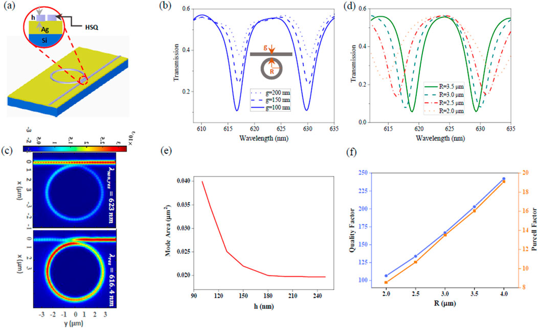
Figure 4. (A) Sketch of the DLSSP-WRR. (B) Transmission spectrum of the HSQ DLSPP-loaded ring-resonator cavity with a 2.5 µm radius, showing spectra for separation gaps of 200 nm, 150 nm, and 100 nm. (C) Full profile of the structure at the resonant wavelength of 616.4 nm and the non-resonant wavelength of 623 nm, for a separation gap of 100 nm. (D) Mode area as a function of HSQ thickness. (E) Calculated mode area as a function of HSQ thickness. (F) Quality factor and Purcell factor as functions of ring radius. In the transmission spectra (B), different ring radii (2.0, 2.5, 3.0, and 3.5 µm) are displayed. The wavelength range from 610 nm to 635 nm is plotted to highlight the transmission characteristics at various separations and ring radii.
Conclusion
We have introduced the design and simulation of a polymer-based Bragg grating cavity with a strip-loaded waveguide. The optimal parameters for this design include a mode volume of
Data availability statement
The raw data supporting the conclusions of this article will be made available by the authors, without undue reservation.
Author contributions
KS: Formal Analysis, Investigation, Methodology, Software, Writing–original draft, Writing–review and editing. FM: Formal Analysis, Investigation, Methodology, Software, Writing–original draft, Writing–review and editing. HS: Conceptualization, Formal Analysis, Funding acquisition, Investigation, Resources, Software, Supervision, Validation, Visualization, Writing–original draft, Writing–review and editing.
Funding
The author(s) declare that financial support was received for the research, authorship, and/or publication of this article. This work was funded by the UKRI Strength in Places Fund programme Smart Nano NI, and the Engineering and Physical Sciences Research Council (EPSRC) under grant number EP/S023321/1.
Conflict of interest
The authors declare that the research was conducted in the absence of any commercial or financial relationships that could be construed as a potential conflict of interest.
Publisher’s note
All claims expressed in this article are solely those of the authors and do not necessarily represent those of their affiliated organizations, or those of the publisher, the editors and the reviewers. Any product that may be evaluated in this article, or claim that may be made by its manufacturer, is not guaranteed or endorsed by the publisher.
References
1. Briegel HJ, Browne DE, Dür W, Raussendorf R, Van den Nest M. Measurement-based quantum computation. Nat Phys (2009) 5:19–26. doi:10.1038/nphys1157
2. Azuma K, Tamaki K, Lo H-K. All-photonic quantum repeaters. Nat Commun (2015) 6:6787. doi:10.1038/ncomms7787
3. Kołodyński J, Máttar A, Skrzypczyk P, Woodhead E, Cavalcanti D, Banaszek K, et al. Device-independent quantum key distribution with single-photon sources. (2018) doi:10.48550/arXiv.1803.07089
4. Giovannetti V, Lloyd S, Maccone L. Advances in quantum metrology. Nat Photon (2011) 5:222–9. doi:10.1038/nphoton.2011.35
5. Meyer-Scott E, Silberhorn C, Migdall A. Single-photon sources: approaching the ideal through multiplexing. Rev Scientific Instr (2020) 91:041101. doi:10.1063/5.0003320
6. Somaschi N, Giesz V, De Santis L, Loredo JC, Almeida MP, Hornecker G, et al. Near-optimal single-photon sources in the solid state. Nat Photon (2016) 10:340–5. doi:10.1038/nphoton.2016.23
7. Siampour H, O’Rourke C, Brash AJ, Makhonin MN, Dost R, Hallett DJ, et al. Observation of large spontaneous emission rate enhancement of quantum dots in a broken-symmetry slow-light waveguide. npj Quan Inf (2023) 9:15. doi:10.1038/s41534-023-00686-9
8. Shandilya PK, Flagan S, Carvalho NC, Zohari E, Kavatamane VK, Losby JE, et al. Diamond integrated quantum nanophotonics: spins, photons and phonons. J Lightwave Technol (2022) 40:7538–71. doi:10.1109/jlt.2022.3210466
9. Siampour H, Kumar S, Davydov VA, Kulikova LF, Agafonov VN, Bozhevolnyi SI. On-chip excitation of single germanium vacancies in nanodiamonds embedded in plasmonic waveguides. Light: Sci and Appl (2018) 7:61. doi:10.1038/s41377-018-0062-5
10. Iles-Smith J, McCutcheon DPS, Nazir A, Mørk J. Phonon scattering inhibits simultaneous near-unity efficiency and indistinguishability in semiconductor single-photon sources. Nat Photon (2017) 11:521–6. doi:10.1038/nphoton.2017.101
11. Hu S, Weiss SM. Design of photonic crystal cavities for extreme light concentration. ACS Photon (2016) 3:1647–53. doi:10.1021/acsphotonics.6b00219
12. Siampour H, Dan Y. Si nanowire phototransistors at telecommunication wavelengths by plasmon-enhanced two-photon absorption. Opt Express (2016) 24:4601–9. doi:10.1364/oe.24.004601
13. Guimbao J, Sanchis L, Weituschat L, Manuel Llorens J, Song M, Cardenas J, et al. Numerical optimization of a nanophotonic cavity by machine learning for near-unity photon indistinguishability at room temperature. ACS Photon (2022) 9:1926–35. doi:10.1021/acsphotonics.1c01651
14. Malkiel I, Mrejen M, Nagler A, Arieli U, Wolf L, Suchowski H. Plasmonic nanostructure design and characterization via Deep Learning. Light: Sci and Appl (2018) 7:60. doi:10.1038/s41377-018-0060-7
15. Piggott AY, Lu J, Lagoudakis KG, Petykiewicz J, Babinec TM, Vučković J. Inverse design and demonstration of a compact and broadband on-chip wavelength demultiplexer. Nat Photon (2015) 9:374–7. doi:10.1038/nphoton.2015.69
16. Siampour H, Nezhad AZ. Revealing the invisible: imaging through non-radiating subspace. J Opt Photon Res (2024). doi:10.47852/bonviewjopr42022785
17. Coste N, Fioretto DA, Belabas N, Wein SC, Hilaire P, Frantzeskakis R, et al. High-rate entanglement between a semiconductor spin and indistinguishable photons. Nat Photon (2023) 17:582–7. doi:10.1038/s41566-023-01186-0
18. Cogan D, Su Z-E, Kenneth O, Gershoni D. Deterministic generation of indistinguishable photons in a cluster state. Nat Photon (2023) 17:324–9. doi:10.1038/s41566-022-01152-2
19. Siampour H, Wang O, Zenin VA, Boroviks S, Siyushev P, Yang Y, et al. Ultrabright single-photon emission from germanium-vacancy zero-phonon lines: deterministic emitter-waveguide interfacing at plasmonic hot spots. Nanophotonics (2020) 9:953–62. doi:10.1515/nanoph-2020-0036
20. Siampour H, Kumar S, Bozhevolnyi SI. Chip-integrated plasmonic cavity-enhanced single nitrogen-vacancy center emission. Nanoscale (2017) 9:17902–8. doi:10.1039/c7nr05675c
21. Liu F, Brash AJ, O’Hara J, Martins LMPP, Phillips CL, Coles RJ, et al. High Purcell factor generation of indistinguishable on-chip single photons. Nat Nanotechnology (2018) 13:835–40. doi:10.1038/s41565-018-0188-x
22. Löbl MC, Söllner I, Javadi A, Pregnolato T, Schott R, Midolo L, et al. Narrow optical linewidths and spin pumping on charge-tunable close-to-surface self-assembled quantum dots in an ultrathin diode. Phys Rev B (2017) 96:165440. doi:10.1103/physrevb.96.165440
23. Dreeßen CL, Oullet-Plamondon C, Tighineanu P, Zhou X, Midolo L, Sørensen AS, et al. Suppressing phonon decoherence of high performance single-photon sources in nanophotonic waveguides. Quan Sci Technology (2019) 4:015003. doi:10.1088/2058-9565/aadbb8
24. Riblet HJ. A mathematical theory of directional couplers. Proc IRE (1947) 35:1307–13. doi:10.1109/jrproc.1947.233573
25. Siampour H, Kumar S, Bozhevolnyi SI. Nanofabrication of plasmonic circuits containing single photon sources. ACS Photon (2017) 4:1879–84. doi:10.1021/acsphotonics.7b00374
26. Mrejen M, Suchowski H, Hatakeyama T, Wang Y, Zhang X. Experimental realization of two decoupled directional couplers in a subwavelength packing by adiabatic elimination. Nano Lett (2015) 15:7383–7. doi:10.1021/acs.nanolett.5b02790
27. Peruzzo A, Shadbolt P, Brunner N, Popescu S, O’Brien JL. A quantum delayed-choice experiment. Science (2012) 338:634–7. doi:10.1126/science.1226719
28. Takagi A, Jinguji K, Kawachi M. Wavelength characteristics of (2*2) optical channel-type directional couplers with symmetric or nonsymmetric coupling structures. J Lightwave Technol (1992) 10:735–46. doi:10.1109/50.143072
29. Kruse KL, Middlebrook CT. Fan-out routing and optical splitting techniques for compact optical interconnects using single-mode polymer waveguides. J Mod Opt (2015) 62:S1–S10. doi:10.1080/09500340.2014.983197
30. Miyatake Y, Toprasertpong K, Takagi S, Takenaka M. Design of compact and low-loss S-bends by CMA-ES. Opt Express (2023) 31:43850–63. doi:10.1364/oe.504866
31. Holmgaard T, Chen Z, Bozhevolnyi SI, Markey L, Dereux A, Krasavin AV, et al. Bend- and splitting loss of dielectric-loaded surface plasmon-polariton waveguides. Opt Express (2008) 16:13585–92. doi:10.1364/oe.16.013585
32. Kumar A, Aditya S. Performance of S-bends for integrated-optic waveguides. Microwave Opt Technology Lett (1998) 19:289–92. doi:10.1002/(sici)1098-2760(199811)19:4<289::aid-mop13>3.0.co;2-y
33. Doughan I, Oyemakinwa K, Ovaskainen O, Roussey M. Strip-loaded Mach–Zehnder interferometer for absolute refractive index sensing. Scientific Rep (2024) 14:3064. doi:10.1038/s41598-024-53326-3
34. Heiblum M, Harris J. Analysis of curved optical waveguides by conformal transformation. IEEE J Quan Electronics (1975) 11:75–83. doi:10.1109/jqe.1975.1068563
35. Holmgaard T, Chen Z, Bozhevolnyi SI, Markey L, Dereux A. Design and characterization of dielectric-loaded plasmonic directional couplers. J Lightwave Technol (2009) 27:5521–8. doi:10.1109/JLT.2009.2031654
36. Chen Z, Holmgaard T, Bozhevolnyi SI, Krasavin AV, Zayats AV, Markey L, et al. Wavelength-selective directional coupling with dielectric-loaded plasmonic waveguides. Opt Lett (2009) 34:310–2. doi:10.1364/ol.34.000310
Keywords: nanophotonics and photonic crystals, quantum, spin qubit, solid-state, optics and photonics
Citation: Snow K, Moradiani F and Siampour H (2024) Strip-loaded nanophotonic interfaces for resonant coupling and single-photon routing. Front. Phys. 12:1475071. doi: 10.3389/fphy.2024.1475071
Received: 02 August 2024; Accepted: 25 September 2024;
Published: 10 October 2024.
Edited by:
Chong Zu, Washington University in St. Louis, United StatesReviewed by:
Wengang Zhang, Beijing academy of quantum information science, ChinaDe-Sheng Li, Hunan Institute of Engineering, China
Copyright © 2024 Snow, Moradiani and Siampour. This is an open-access article distributed under the terms of the Creative Commons Attribution License (CC BY). The use, distribution or reproduction in other forums is permitted, provided the original author(s) and the copyright owner(s) are credited and that the original publication in this journal is cited, in accordance with accepted academic practice. No use, distribution or reproduction is permitted which does not comply with these terms.
*Correspondence: Hamidreza Siampour, aC5zaWFtcG91ckBxdWIuYWMudWs=