 Yijun Li
 Tianye Ma
- School of Electrical and Automation Engineering, Nanjing Normal University and Jiangsu Key Laboratory of 3D Printing Equipment and Manufacturing, Nanjing, China
This article introduces a novel microstrip filtering balun designed using GaAs Integrated-Passive-Device (IPD) technology, aimed at addressing the needs of millimeter-wave communication applications such as Wireless Personal Area Networks (WPAN) and Wireless Local Area Networks (WLAN). The design leverages a wavelength transmission line for phase inversion and coupling structures to enhance frequency selectivity. A prototype was fabricated and tested, demonstrating a center frequency of 45.6 GHz, a relative bandwidth of 59.2%, and a phase difference of 180° (±7.0°) between the output ports. Simulations and measurements confirm the design’s excellent bandwidth and selectivity, showcasing its potential for integration into compact, high-performance communication systems.
1 Introduction
System-level integration and packaging represent some of the most promising technologies due to their potential to enhance performance, reduce size, and reduce costs [1, 2]. The IPD technology is essential for achieving system-level integration [3, 4], offering enhanced manufacturing precision compared to technologies such as Low Temperature Co-fired Ceramic (LTCC) [5], Printed Circuit Boards (PCB) [6]. Numerous IPD designs have been published and integrated into various integrated circuit systems [3–8].
Baluns, which transform electromagnetic waves from balanced to unbalanced transmission lines, or vice versa, are widely utilized in wireless systems. Typically, a balun comprises a power divider and a phase shifter. For example, in [9], a balun based on Marchand structure was introduced in recent study, albeit relatively larger in size. Another study [10] explored an out-of-phase filtering power divider, incorporating a balun filter and a four-port network, achieving a relative bandwidth of 58%. However, its bandwidth and size could be further improved. Additionally, a significant design utilized a multi-layer LTCC structure to achieve good isolation and frequency selectivity while maintaining a relatively small size [11]. Nonetheless, its complex and large structure increased integration costs with semiconductor chips.
This paper presents a novel design of a microstrip filtering balun in GaAs IPD technology, targeting the 50 GHz center frequency to meet the demands of millimeter-wave high-speed communication applications, such as WPAN and WLAN. The proposed design features a unique circuit topology that achieves high integration through IPD technology, realizes phase inversion using a one-wavelength transmission line, and utilizes a U-shaped resonator combined with short-circuited lines to not only expand bandwidth but also introduce two transmission zeros, enhancing frequency selectivity. Simulations and measurements verify the effectiveness of this approach. This new balun design exhibits strengths in size, bandwidth and frequency selectivity, while maintaining a simple structure, thus presenting potential advantages for numerous miniaturized communication systems.
2 Configuration of the proposed microwave filtering balun
Figure 1 illustrates the layout of the proposed microstrip filtering balun, which consists of a feeding microstrip line, two U-shaped microstrip resonators, and an output microstrip line connecting two output ports. The input electromagnetic wave, fed in from Port 1, propagates through the feeding microstrip line with a length of approximately one wavelength. Due to the opposite electric field directions on each half of the transmission line, two U-shaped resonators are excited with opposite phases. A portion of the input signal travels through the wavelength-long microstrip, and then continues to propagate along a quarter-wavelength short-ended line, introducing a transmission zero (TZ) point to improve selectivity. The two U-shaped resonators, excited in opposite phases through coupling, enhance the bandwidth by resonating in multiple modes and transmit signal to the output ports through a coupling microstrip line. Consequently, the device gets filtering, power dividing and phase inversion functions, forming a broadband balun. Figure 2 shows the equivalent circuit of the proposed design, corresponding to the layout in Figure 1.
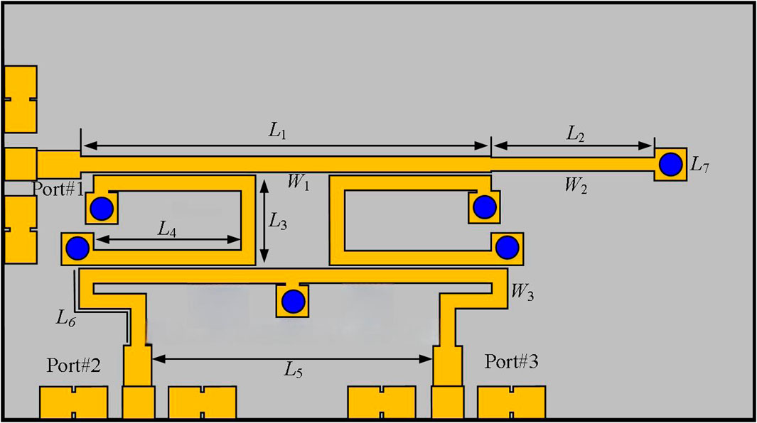
Figure 1. Layout of the proposed filtering balun.
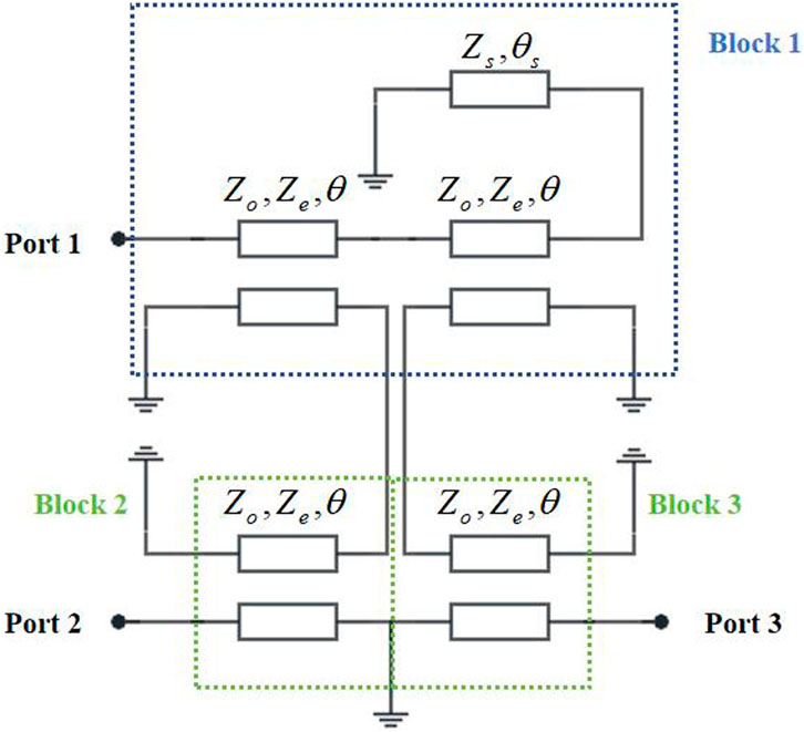
Figure 2. Schematic diagram of the proposed filtering balun.
3 Design and analysis of the proposed microwave filtering balun
As shown in Figure 2, the balun design consists of two U-shaped resonators arranged in a mirror-symmetric configuration. Each resonator forms a section of microstrip coupler with the input microstrip line and another section of microstrip coupler with the output microstrip line. Electromagnetic energy is transferred from the input microstrip line to the output microstrip line via the U-shaped resonators. The design includes a total of four microstrip couplers, each with identical line width, gap width, and length, ensuring complete uniformity among the four couplers. Moreover, each coupler is a symmetric structure, enabling even-/odd-mode analysis method to be applied. Therefore, each coupler can be characterized by its odd-mode impedance
Where the ABCD-matrix of a microstrip coupler can be written as
The Z-matrix of the three-port network, represented as Block 1 in Figure 2, can be expressed as follows:
Where
Therefore, the theoretical response of the proposed structure can be calculated by applying Equations 1–8. Then, the initial value of the balun design can be obtained.
To better analyze the frequency response of the proposed filtering balun, we draw an equivalent circuit diagram, displayed as Figure 3, based on the schematic diagram in Figure 2. Thus, the even-/odd-mode method can be applied to derive the filtering and isolation functions of this out-of-phase power divider [13]. The three-port network in Figure 3 has parameters
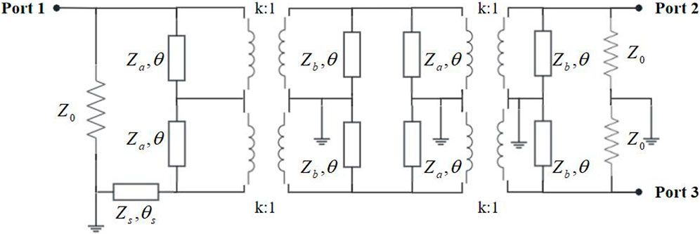
Figure 3. The equivalent circuit diagram of the proposed filtering balun.
Since the differential output of a balun is of interest, the odd-mode equivalent circuit, shown in Figure 4, is analyzed to determine the TZs. The odd-mode equivalent circuit consists of two impedance-matching transmission lines, a short-circuited impedance resonator, three shunt short-circuited stubs and two transformers. In order to obtain the TZs, the input impedances of the shunt stubs, written as follows, must be equal to zero [15, 16].
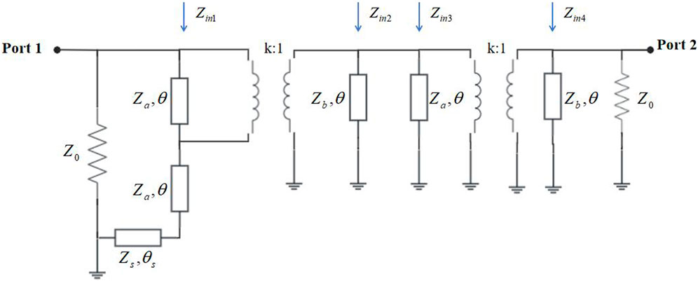
Figure 4. Bisected odd-mode equivalent circuit of the proposed filtering balun.
In this design, the electric length is set to
By intentionally positioning the TZs near the passband, the filtering response of the balun can be further enhanced with improved selectivity. Subsequently, the parameter values of the balun design are slightly adjusted using numerical simulations, to achieve better filtering performance and out-of-phase response. This approach ensures the realization of the desired filtering balun design.
4 Results and discussion
To validate the analysis, a prototype was designed and fabricated on a compound semiconductor substrate. The structure consists of four thin layers of SiN (with respective thicknesses of 3.6 μm, 2.19 μm, 0.83 μm, and 0.376 μm, from top to bottom) deposited on a 100 μm-thick GaAs substrate, with a metal ground plane on its underside. As we are targeting at a center frequency of 50 GHz, the optimized parameters of the balun are as follows (in mm): L1 = 1.01089, L2 = 0.402, L3 = 0.2171, L4 = 0.3623, L5 = 0.6922, L6 = 0.317, L7 = 0.08, W1 = 0.0377, W2 = 0.0328, W3 = 0.0377.
The balun prototype was simulated by Ansys HFSS. The simulated S parameters are depicted in Figure 5, indicating a bandpass center frequency of 50 GHz and a relative bandwidth of 65%. Notably, the TZs are located at 25 GHz and 85 GHz.The prototype and the test setup are shown in Figure 6. The VNA (vector network analyzer) was extended to the desired frequency range using a pair of frequency extension modules. The balun prototype was placed on a probe station, connected to a metallic waveguide via a CPW (coplanar waveguide) probe. The waveguide was then connected to the frequency extension module of the VNA through its waveguide port, enabling the measurement of S parameters. The measured S parameters are shown as Figure 7. Due to the limitation posed by the available measuring equipment, only the S-parameters up to 67 GHz was tested. Figure 7 shows that the measured passband spans from 32.1 GHz to 59.1 GHz, with a relative bandwidth of 59.2%.These measured results validate the filtering performance of this design and affirm the effectiveness of the proposed analysis. Multiple factors may contribute to the difference between measurements and simulations, such as the substrate material, the measurement process and the fabrication error. The measured minimum insertion loss is 0.25 dB (excluding the theoretical 3 dB insertion loss due to power dividing). Furthermore, Figure 8 shows the simulated and measured amplitude imbalance and phase difference, indicating that the measured phase difference between the two output ports is 180°(±7.0°), and the amplitude imbalance is lower than 1.06 dB. Comparisons are made with several previous works in Table 1, showing that our work achieves a broader bandwidth with a good selectivity.
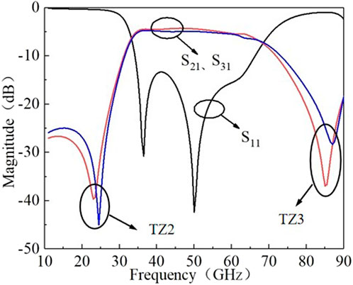
Figure 5. The simulated S parameters of the proposed filtering balun.
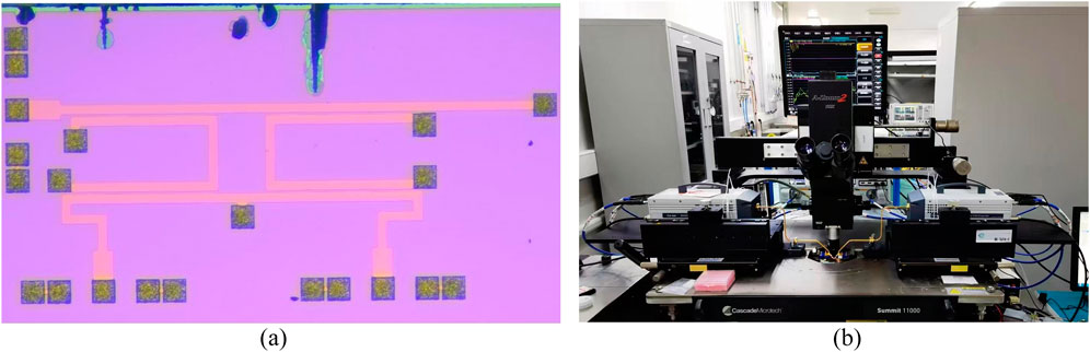
Figure 6. The (a) manufactured balun prototype and (b) the measuring setup picture.
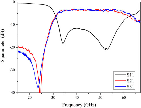
Figure 7. The measured S parameters of the proposed balun.
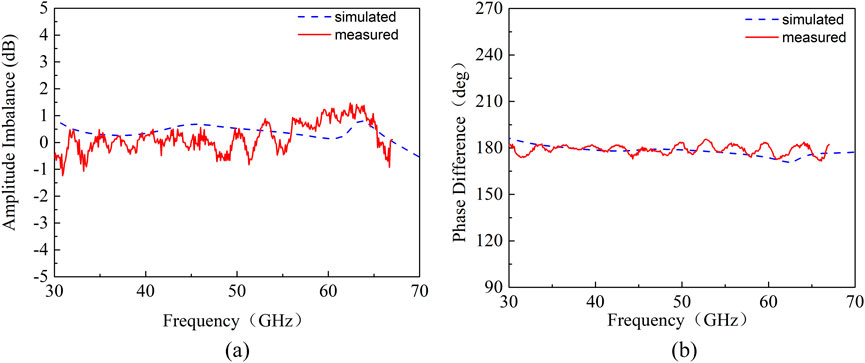
Figure 8. The simulated (a) amplitude and (b) phase difference between two output ports.
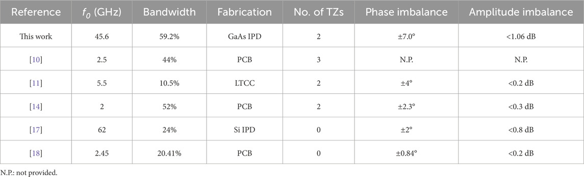
Table 1. Comparisons with previous works.
5 Conclusion
This article presents a novel design of a microstrip filtering balun, introducing a new balun topology that utilizes a wavelength transmission line and coupling structures to achieve phase inversion property and frequency selectivity. The S-parameters and frequency response of the balun were analyzed in detail, and an IPD balun prototype was designed, fabricated and tested on a GaAs substrate. The simulated and measured results confirm that the proposed balun exhibits excellent bandwidth, strong phase inversion properties, and high frequency selectivity. Moreover, the proposed balun realized a higher level of integration by adopting IPD technology, and a combination of wide bandwidth and high selectivity, compared to previous works [10, 11, 15]. This balun, characterized by its compactness, feasibility, ease of integration, broadband performance, and good frequency selectivity, demonstrates significant advantages for modern miniaturized communication systems.
Data availability statement
The raw data supporting the conclusions of this article will be made available by the authors, without undue reservation.
Author contributions
YL: Writing – original draft. JN: Writing – original draft. SL: Writing – original draft. QH: Writing – review and editing. JT: Writing – review and editing. NL: Writing – review and editing. TM: Writing – original draft, Writing – review and editing.
Funding
The author(s) declare that financial support was received for the research and/or publication of this article. This work was supported by the Joint Foundation of Key Laboratory of Shanghai Jiao Tong University-Xidian University, Ministry of Education, under Grant LHJJ/2024-6.
Conflict of interest
The authors declare that the research was conducted in the absence of any commercial or financial relationships that could be construed as a potential conflict of interest.
Generative AI statement
The author(s) declare that no Generative AI was used in the creation of this manuscript.
Publisher’s note
All claims expressed in this article are solely those of the authors and do not necessarily represent those of their affiliated organizations, or those of the publisher, the editors and the reviewers. Any product that may be evaluated in this article, or claim that may be made by its manufacturer, is not guaranteed or endorsed by the publisher.
References
1. Khan MSM, Xi C, Haque MSU, Tehranipoor MM, Asadizanjani N. Exploring advanced packaging technologies for reverse engineering a system-in-package (SiP). IEEE Trans Components, Packaging Manufacturing Technology (2023) 13(9):1360–70. doi:10.1109/tcpmt.2023.3311801
2. Manley M, Victor A, Park H, Kaul A, Kathaperumal M, Bakir MS. Heterogeneous integration technologies for artificial intelligence applications. IEEE J Exploratory Solid-State Comput Devices Circuits (2024) 10:89–97. doi:10.1109/jxcdc.2024.3484958
3. Liu L, Kuo S -M, Abrokwah J, Ray M, Maurer D, Miller M. Compact harmonic filter design and fabrication using IPD technology. IEEE Trans Components Packaging Tech (2007) 30(4):556–62. doi:10.1109/TCAPT.2007.901672
4. Chiang C -W, Wu C -TM, Liu N -C, Liang C -J, Kuan Y -C. A cost-effective W-band antenna-in-package using IPD and PCB technologies. IEEE Trans Components, Packaging Manufacturing Technology (2022) 12(5):822–7. doi:10.1109/tcpmt.2022.3170499
5. Pourzadi A, Adibi A, Mousavi SH, Kouki A. A fast technique for realization of lumped-element values into 3-D physical layout on LTCC. IEEE Trans Components, Packaging Manufacturing Technology (2021) 11(9):1497–505. doi:10.1109/tcpmt.2021.3105867
6. Steele J, Psychogiou D. Compact multilayer PCB-based Marchand baluns with maximized fractional bandwidth. IEEE Access (2024) 12:160982–91. doi:10.1109/access.2024.3487130
7. Chiu T -Y, Li C -H. Low-loss low-cost substrate-integrated waveguide and filter in GaAs IPD technology for terahertz applications. IEEE Access (2021) 9:86346–57. doi:10.1109/access.2021.3089614
8. Cheng J -D, Xia B, Xiong C, Wu L -S, Mao J -F. An unequal wilkinson power divider based on integrated passive device technology and parametric model. IEEE Microwave Wireless Components Lett (2022) 32(4):281–4. doi:10.1109/lmwc.2021.3126850
9. Feng W, Zhu H, Che W, Xue Q. Wideband in-phase and out-of-phase balanced power dividing and combining networks. IEEE Trans Microwave Theor Tech (2014) 62(5):1192–202. doi:10.1109/tmtt.2014.2314441
10. Li L, Mao J, Wu L-S, Tang M, Gu X. A general method for balanced-to-unbalanced filtering out-of-phase power divider design. IEEE Trans Microwave Theor Tech (2019) 67(7):2693–700. doi:10.1109/tmtt.2019.2914107
11. Zhang XY, Liu X-F, Li YC, Zhan W-L, Lu QY, Chen J-X. LTCC out-of-phase filtering power divider based on multiple broadside coupled lines. IEEE Trans Components, Packaging Manufacturing Technology (2017) 7(5):777–85. doi:10.1109/tcpmt.2017.2661997
12. Zhang G, Wang J, Zhu L, Wu W. Dual-mode filtering power divider with high passband selectivity and wide upper stopband. IEEE Microwave Wireless Components Lett (2017) 27(7):642–4. doi:10.1109/lmwc.2017.2711556
13. Mongia RK, Bahl IJ, Bhartia P, Hong JR. RF and microwave coupled-line circuits. Norwood, MA, USA: Artech House (2007).
14. Wang X, Wang J, Shi J, Guo Z -C. Study on packaging of a wideband filtering out-of-phase power divider based on multi-layer stacked striplines. IEEE MTT-S Int Wireless Symp (Iws) (2023). p. 1–4. doi:10.1109/iws58240.2023.10223099
15. Wang X, Wang J, Zhang G, Hong J, Wu W. Design of out-of phase filtering power divider based on slotline and microstrip resonator. IEEE Trans Compon Packag Manuf Technol (2019) 9(6):1094–102. doi:10.1109/tcpmt.2018.2868706
17. Xu L, Sjöland H, Törmänen M, Tired T, Pan T, Bai X. A miniaturized Marchand balun in CMOS with improved balance for millimeter-wave applications. IEEE Microwave Wireless Components Lett (2014) 24(1):53–5. doi:10.1109/LMWC.2013.2288270
Keywords: balun, wideband, integrated-passive-device technology, filtering response, GaAs
Citation: Li Y, Ni J, Li S, Han Q, Tian J, Li N and Ma T (2025) Design of a millimeter-wave wideband filtering balun in GaAs IPD technology. Front. Phys. 13:1555410. doi: 10.3389/fphy.2025.1555410
Received: 04 January 2025; Accepted: 29 May 2025;
Published: 18 June 2025.
Edited by:
Liu Qianwen, Nanjing University of Posts and Telecommunications, ChinaReviewed by:
Zhipeng Xia, Nanjing University of Science and Technology, ChinaYunpeng Lyu, Nanjing University of Posts and Telecommunications, China
Copyright © 2025 Li, Ni, Li, Han, Tian, Li and Ma. This is an open-access article distributed under the terms of the Creative Commons Attribution License (CC BY). The use, distribution or reproduction in other forums is permitted, provided the original author(s) and the copyright owner(s) are credited and that the original publication in this journal is cited, in accordance with accepted academic practice. No use, distribution or reproduction is permitted which does not comply with these terms.
*Correspondence: Tianye Ma, dGlhbnllLm1hQGZveG1haWwuY29t