 Fahad Alghannam
 Nada S. Alharthi
 Mrwan Alayed
- 1Microelectronics and Semiconductors Institute, King Abdulaziz City for Science and Technology (KACST), Riyadh, Saudi Arabia
- 2Advanced Materials Institute, King Abdulaziz City for Science and Technology (KACST), Riyadh, Saudi Arabia
Nd:YAG laser light detection at 1064 nm is widely used in applications requiring high-performance photodiodes to measure low light intensities. This study investigates the impact of light trapping and geometric variations on the responsivity of silicon-based PIN photodiodes at 1064 nm. Simulations using Ansys Lumerical FDTD and CHARGE reveal several key findings. Without diffuse reflectors, the responsivity of the photodiodes aligns with theoretical and literature values of approximately 0.4–0.45 A/W. When rear-side diffuse reflectors are used, larger photodiode dimensions result in higher responsivity, with a peak of 0.58 A/W for photodiodes with a 400 µm thickness. Our simulations suggest that combining light trapping with optimized geometries or side reflectors could surpass the current responsivity ceiling of ∼0.57 A/W, offering a pathway to exceed this limit without sacrificing electrical performance. Also, light trapping reduces the required thickness of Si PIN photodiodes for achieving specific responsivity at 1064 nm. For instance, 100 µm thick photodiodes with diffuse reflectors exhibit a responsivity of approximately 0.31 A/W, compared to 0.28 A/W in 400 µm thick photodiodes without reflectors. However, the enhancement from light trapping diminishes as photodiode thickness increases. Optimal photodiode dimensions for balanced performance are suggested to be a thickness of 200–300 μm and an area of 0.6–2.5 mm2. Experimental validation is recommended to assess texturing-related effects, such as increased dark current or recombination.
1 Introduction
The Nd:YAG laser light (1064 nm wavelength) is critical in various fields, including medicine [1], environmental monitoring [2], spectroscopy [3], and defense and security [4]. Consequently, photodetectors based on different semiconductor materials, such as InGaAsP/InAlAs [5], p-BP/n-PdSe2 [6], InN/GaN [7], TiS3 [8], or silicon [9] have been developed to detect 1064 nm light. The performance of a photodiode in detecting light within a specific wavelength range is primarily determined by its responsivity, defined as the ratio of the photodiode’s output current to the incident optical power [10]. Thus, Silicon-based PIN photodiodes (PDs) are a preferred choice for such near-infrared detection due to their cost-effectiveness, scalability, and seamless integration with Complementary Metal-Oxide-Semiconductor (CMOS) technology and silicon photonics [11]. However, the low absorption coefficient of silicon (∼10 cm−1) in the 1064 nm wavelength range poses a significant challenge for achieving high responsivity, which is essential for applications requiring high sensitivity to low-intensity light, such as environmental sensing or medical diagnostics [12, 13]. To measure low-intensity 1064 nm light using Si photodetectors, a common approach is to employ Si PIN PDs with a thicker substrate and depletion region, increasing the optical path length of the incoming light [12, 14]. However, silicon PIN PDs thicker than 500 µm are impractical due to degraded electrical performance, such as higher noise, slower rise times, and reduced bandwidth [14].
Several strategies have been demonstrated to improve the responsivity of Si PIN PDs at 1064 nm. First, Anti-Reflection Coatings (ARCs) are used to minimize the percentage of reflected light to below 1% (∼30% reflection without ARC) [15]. Second, a rear-side specular reflector can be used to reflect light, thereby extending the optical path length without increasing the thickness of the detector [14]. Third, the optical path length can be maximized without increasing the physical path length, using rear-side texturing to create a diffuse reflector that increases the probability of light being scattered and reabsorbed within the detector, thereby enhancing light trapping [16, 17]. Fourth, the Si PIN photodiode’s temperature can be increased using heat, which increases the silicon’s absorption coefficient [18]. Fifth, the responsivity can be enhanced by optimizing the electrical parameters, such as increasing minority carrier lifetime and diffusion length and operating in full depletion mode (detector thickness Z ≈ depletion region width W) [11, 19]. Lastly, utilizing multiphysics simulation tools, like COMSOL and Ansys, can help in understanding and optimizing the photodiode’s performance by modeling the effects of different designs and operational parameters on electrical and optical characteristics [13, 20].
While techniques like ARCs [15], specular reflectors [14], and texturing [16] could individually enhance responsivity, few studies systematically combine light trapping with geometric optimization (area and thickness) to maximize responsivity at 1064 nm while maintaining electrical performance within practical thickness limits (≤400 μm). This gap drives our study, which uses Ansys Lumerical FDTD and CHARGE to explore the synergistic effects of rear-side diffuse reflectors and dimensional variations, aiming to push responsivity beyond the current ceiling of ∼0.57 A/W reported in the literature [16, 21]. To the best of our knowledge, the combined effects of light trapping and geometric parameters on responsivity at 1064 nm in this context have not been fully addressed in the literature. Thus, we use Ansys Lumerical FDTD and CHARGE to assess how rear-side texturing affects responsivity at 1064 nm across varying Si PIN photodiode dimensions. Therefore, we have incorporated ARCs, rear-side texturing, and full depletion mode in our simulated Si PIN PDs to figure out the maximum achievable responsivity of light detection at 1064 nm due to light trapping optimization. Simultaneously, our Si PIN PDs are designed with dimensional constraints to preserve favorable electrical characteristics, such as low noise, fast response times, and high bandwidth.
In this work, we have investigated how light trapping and geometric parameters of Si PIN PDs affect their responsivity, considering trade-offs in response time, bandwidth, and noise (e.g., dark current). Therefore, in section two, we briefly define the primary optical and electrical characteristics and the impacts of light trapping. Section three describes the setup for three structures of Si PIN PDs and specifies the parameters of the optoelectronic simulation. In section four, we present the findings and discuss the results.
2 Photodiode characteristics
This section outlines the optical and electrical characteristics of silicon PIN PDs critical to interpreting the simulation results at 1064 nm. These properties, such as responsivity, dark current, noise equivalent power (NEP), and rise time, define the performance trade-offs analyzed in this study. Section 2.3 also discusses the feasibility, impact, and fabrication methods of light trapping using specific micro- and nanostructures.
2.1 Optical characteristics
The responsivity is the main optical characteristic of a photodiode, and it describes its ability to convert incident optical power into electrical current and is the primary metric evaluated here. It is expressed as [15]:
Where ηe is the external quantum efficiency, q is the electron charge, h is Planck’s constant, and f is the frequency of the optical signal. f = c/λ where c is the speed of light and λ is the wavelength of the incident light. For silicon at 1064 nm, the R(λ) for a photodiode depends heavily on ηe, as (q, λ, h, and c) are constants. Theoretically, with ηe = 100% (every photon absorbed produces a carrier), the maximum responsivity of a silicon PIN photodiode at 1064 nm would be:
Where Rf is the front reflection (∼35% for bare silicon at 1064 nm, leading to ηe = 0.65 ηi [23], reducible to <1% with ARCs [15]) and ηi is the internal quantum efficiency. The ηi represents the carriers detected within the detector divided by photons entering the front surface. The ηi can be calculated using the following formula [10]:
Where α is the absorption coefficient (α = 10 cm−1 at 1064 nm wavelength for silicon), PD(x) is the carrier detection probability, and x is the thickness of the depletion region. In the ideal case, PD(x) = 1. Thus, the formula can be simplified to [10]:
Thus, a thicker depletion region can substantially enhance the ηi of silicon PDs at 1064 nm. However, increasing the physical thickness beyond 500 µm is impractical due to degradation in essential characteristics like Idark, NEP, and rise time τR [24]. Also, x can be increased directly to be almost equal to the photodiode thickness (Z ≈ x) by operating the photodiode in full depletion condition to achieve higher responsivity. In full depletion condition, the photodiode operates effectively as a photodetector. Thus, by substituting ηe from Equations 2–4 into Equation 1, the responsivity R(λ) at 1064 nm can be estimated using the following formula:
From Equation 5, with ideal front reflection (Rf ≤ 0.01) and physical thickness (Z = 0.5 mm), the responsivity of Si photodiode RA ≈ 0.337 A/W, which is much less than the reported responsivity (≥0.4 A/W) at 1064 nm for state of the art YAG PDs shown in Table 1. Therefore, it is necessary to use reflectors to increase the optical path length of the light within the Si PIN PDs. In full depletion condition, when a rear side specular reflector is used, the responsivity R(λ) at 1064 nm can be estimated using the following formula [10]:
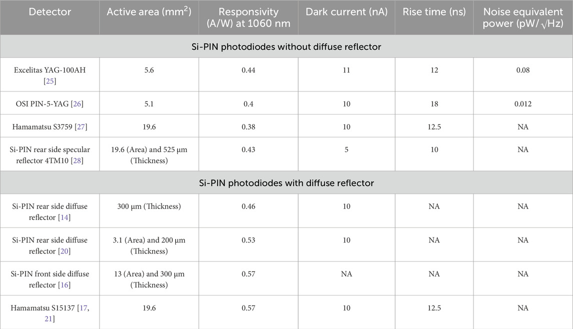
Table 1. Comparison of main features of the reported YAG photodiodes.
However, based on Equation 6, the responsivity does not exceed 0.5 A/W (far below the theoretical maximum responsivity) of a fully depleted Si PIN photodiode with (Rf ≤ 0.01) with an ideal rear side specular reflector (Rr ≈ 0.9) and (Z = 0.5 mm).
2.2 Electrical characteristics
While high responsivity is critical for Si PIN PDs, other electrical characteristics are also essential for performance in low light intensity measurements, such as:
a. Low dark current Idark: In wide depletion regions PDs, dark current is dominated by the recombination-generation current IR-G, which is related to the product of area A and thickness Z, as shown in the equation [19, 29]:
Where ni is the silicon intrinsic concentration (1010 cm−3 at 300K), τ0 is the carrier lifetime, A is the photodiode area, and Z is the photodiode thickness.
b. Low Noise Equivalent Power (NEP): The optical power needed to get a signal-to-noise ratio of 1. The NEP of a photodiode is defined as [30, 31]:
Where q, Idark, and R are electron charge, dark current, and responsivity, respectively.
c. Short Rise time τR and high Bandwidth (BW) represent the photodiode response speed. Bandwidth has an inverse relationship with the rise time according to the following equations [32–34]:
Where BW, tR, tT, and tC are bandwidth, rise time, transit time, and RC time constant, respectively. In full depletion condition:
Where VR and εSi are reverse bias voltage and the absolute permittivity of silicon, respectively. Therefore, most characteristics of Si PIN PDs can be roughly estimated using Equations 7–12. These equations also highlight how geometries directly influence the characteristics of Si PIN PDs.
2.3 Feasibility and impact of light trapping
Light trapping techniques, such as surface texturing, significantly boost the responsivity of silicon PIN PDs up from the baseline range of ∼0.45 A/W at 1064 nm, as shown in Table 1. However, texturing for light trapping may introduce electrical drawbacks, such as surface recombination, elevated noise, increased dark current, and longer response times, necessitating further investigations in fabricated devices [35]. Nevertheless, in the reported silicon PIN PDs, see Table 1, the responsivity at 1064 is improved significantly without degradation of the electrical characteristics [21]. On the other hand, inverted pyramid light-trapping structures, a nanoscale texture often used in black silicon (BSi), can be fabricated via lithography or metal-assisted chemical etching (MACE), with copper-assisted method [35], and Tang et al. highlight their adaptability through temperature-controlled sizing [36]. MACE is a scalable and cost-effective method, with variations like copper-assisted chemical etching being particularly effective for creating these structures [35].
3 Simulation methods
We studied the impacts of rear-side texturing on Si PIN PDs through a two-stage multiphysics simulation process, as explained in [37, 38]. Initially, we simulated the optical properties of the PDs using ANSYS Lumerical Finite-Difference Time Domain (FDTD). Next, we exported the results from ANSYS Lumerical FDTD into ANSYS Lumerical CHARGE to simulate the electrical properties. Figure 1 illustrates the simulation workflow for photodiode devices in this work.
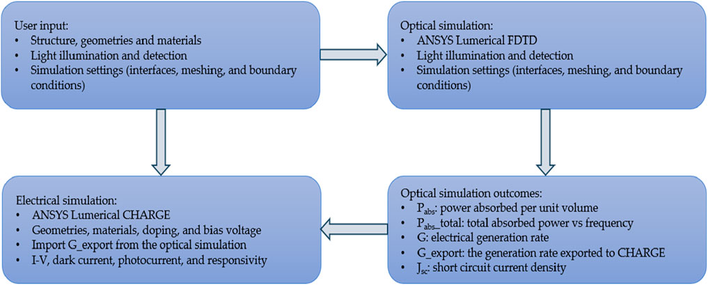
Figure 1. Simulation workflow for photodiodes using ANSYS Lumerical FDTD and CHARGE.
3.1 Photodiode structures
Three distinct Si PIN photodiode configurations were simulated and evaluated:
a. Structure 1: No rear-side reflection (Rr = 0).
b. Structure 2: Specular rear-side reflection using a flat aluminum cathode (Rr≈ 0.85 or 85%).
c. Structure 3: Diffuse rear-side reflection using pyramidal structures (triangle in 2D with 53° angles between sides and base).
For all three structures, simulations were performed with varying areas and thicknesses, as outlined in Table 2. A total of 16 PDs with different geometries were simulated for each structure. The responsivity results from structures 1 and 2 serve to validate the accuracy of our simulation approach and compare them with those of structure 3. The responsivity values are analyzed to evaluate the impact of area, thickness, and light trapping via rear-side diffuse reflection. Each photodiode is labeled according to its geometric dimensions to ensure clarity, as outlined in Table 2.
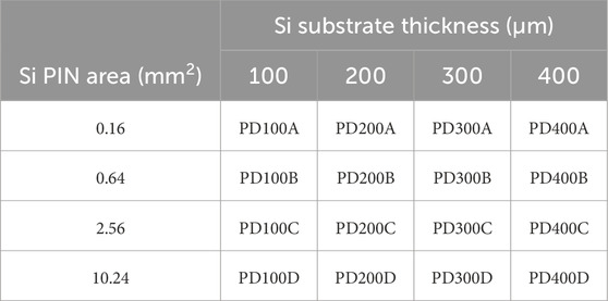
Table 2. Dimensions of the simulated Si PIN photodiodes.
3.2 Optical simulation
The key parameters of the optical simulation include boundary conditions, mesh configuration, and the position of the laser source. First, Perfectly Matched Layer (PML) boundary conditions are applied to absorb incident light with minimal reflection and to match the impedance with surrounding materials, thereby reducing reflections [39]. Second, Conformal Variant 0 is used as the mesh refinement method, leveraging Conformal Mesh Technology (CMT) for the aluminum to ensure better accuracy at the metal interfaces and the complex geometry of the pyramids [40]. Mesh sizes down to 5 nm at interfaces and up to 50 nm in the substrate ensure ±2% photocurrent accuracy [40], though finer meshes (<5 nm) could further reduce errors at a higher computational cost [41]. Third, the light source is positioned at the same height as the highest part of the PIN photodiode, with the anodes 400 nm above the silicon surface (270 nm above the upper layer of the ARC). The simulation setup is illustrated in Figure 2.
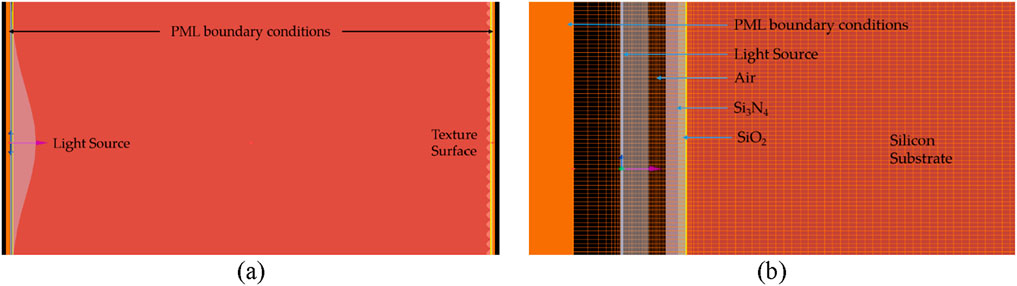
Figure 2. Cross-section of the simulated photodiodes: (a) front and rear side interfaces, and (b) components of the front side interface for all three structures.
3.2.1 Front-side interface
All simulations of the PDs use normal incidence (θ = 0°), a narrow wavelength band (1062 nm–1067 nm), and a Gaussian light source, as shown in Figure 2b. The optical power of the source is adjusted by multiplying the fixed light intensity by the variable areas of the PDs. Therefore, the optical power for PDs A, B, C, and D is 0.16 µW, 0.64 µW, 2.56 µW, and 10.24 µW, respectively. Additionally, the beam diameters correspond to 20% of the PDs width, with values of 80 μm, 160 μm, 320 μm, and 640 µm for PDs A, B, C, and D, respectively. Two layers of Anti-Reflection Coatings (ARCs) have been used in this work. The upper layer is Si3N4, and the lower layer is SiO2, where the thickness is 80 nm and 50 nm, respectively [34]. This ARC assures little reflection of the incoming light at 1064 nm (≤0.1%), as shown in Figure 3a. Moreover, This ARC is tolerant to the variation of layer thicknesses during the fabrication process. Figure 3b demonstrates that the reflection is less than 3% if the total thickness of both layers ranges from (110 nm–150 nm).
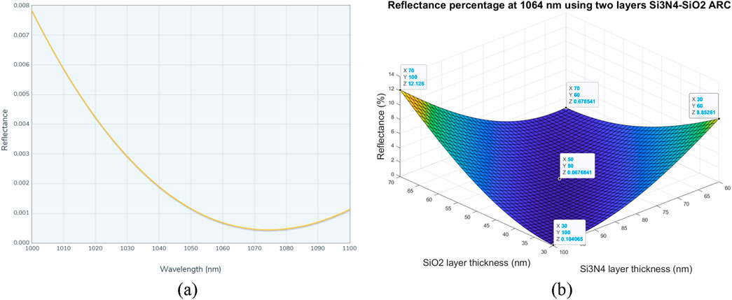
Figure 3. The reflectance percentage at 1064 nm using two layers (a) Si3N4-SiO2 ARC, where Si3N4 is 80 nm, and SiO2 is 50 nm, and (b) Si3N4-SiO2 [Si3N4 80 nm ± 20 nm] and [SiO2 50 nm ± 20 nm].
3.2.2 Rear side interface
For Structure 1, which has no rear-side reflection (Rr = 0), an absorber boundary condition is applied to the rear side, the supposed position of the cathode, to prevent light reflection, as shown in Figure 4a. In Structure 2, where the rear-side reflection is Rr = 0.85, a flat aluminum cathode covers the entire rear side of the photodiode, with a thickness of 400 nm, as depicted in Figure 4b. For Structure 3, the PDs feature textured rear surfaces with aluminum pyramids (∼0.66 µm height) on the flat aluminum cathode (0.4 µm thickness). These textures have been formed using aluminum pyramids (triangles in 2D with 53° angles between sides and base), as illustrated in Figure 4c. This pyramid structure was selected because it can be fabricated using black silicon methods, as mentioned in Section 2.3, and subsequent metallization techniques [42–44]. Specifically, inverted pyramid arrays can be created on the rear side of a silicon wafer through etching methods described in the literature [45], and the inverted pyramids can be filled with highly reflective metals, such as aluminum, via metallization. Figure 4 shows the cross-sectional views of the rear-side setups for all three photodiode configurations.
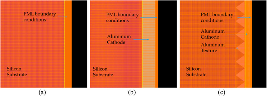
Figure 4. Cross-sectional views of the rear-side structures of the photodiodes: (a) no rear side reflection (Structure 1), (b) rear side specular reflection using flat surface of the aluminum cathode (Structure 2), and (c) rear side with texture aluminum pyramids layer as a diffuse reflector (Structure 3).
3.3 Electrical simulation
Before conducting the electrical simulation, certain parameters need to be established to optimize silicon PIN PDs for detecting Nd:YAG light and to align their electrical characteristics with those of the PDs listed in Table 1. The preliminary estimated results are displayed in Figure 5.
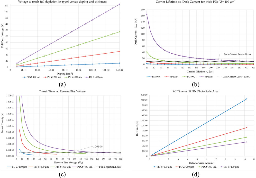
Figure 5. Parameters of the simulated photodiodes: (a) required bias voltage to operate in full depletion mode versus the doping levels of the intrinsic region NB for Si PIN photodiodes with thicknesses ranging from 100 µm up to 400 μm, (b) dark current values for photodiodes vs carrier lifetime of the silicon substrate, (c) transit time vs reverse voltage, and (d) RC time vs photodiode area.
First, the doping concentration of the [n-type] intrinsic region NB in a silicon PIN diode for 1064 nm detection should be kept low, around 1012, to ensure full depletion mode at low reverse bias voltage, achieve high quantum efficiency and minimize dark current and recombination [13]. Figure 5a illustrates the relationship between the bias voltage required for full depletion and the NB for the selected thicknesses in this study. Furthermore, Figure 5a also demonstrates that the NB must be low enough to ensure full depletion and allow the depletion region to extend through the entire intrinsic region when a reverse bias is applied. Since we aim to unify all parameters for all PDs’ structures, an intrinsic doping concentration of NB = 1.1 × 1012 cm−3 was selected, tailored for PDs up to 0.4 mm thickness and 10.24 mm2 area. For instance, at this NB, the required reverse bias voltage to reach full depletion for PD400 (W = 0.4 mm thickness) is approximately 140V, which can be estimated using the equation [46]:
Where W is the depletion width, the silicon permittivity ɛSi = 10−12 F/cm, and the built-in voltage Vbi = 0.7 V. Therefore, based on Equation 13, the chosen NB allows Si PIN PDs to achieve full depletion mode at practical reverse bias voltage levels (≤140 V). Additionally, this NB doping improves thermal stability at elevated temperatures (up to 60°C), which is essential for reliability in harsh environments, as increased NB mitigates the effect of rising intrinsic carrier concentration ni. The ni represents the number of thermally generated electron-hole pairs in an undoped semiconductor and is described by Equation 14 [46]:
Where, for silicon, B is the material constant
Second, the required carrier lifetime of silicon to achieve a dark current as low as the reported PDs in Table 1 (IDark ≤ 10 nA). As shown in Figure 5b, our analysis indicates that the required carrier lifetimes for photodiodes PD400A, PD400B, PD400C, and PD400D are greater than 5 µs, 20 µs, 80 µs, and 320 µs, respectively. Third, the impact of the operating reverse bias voltage and area of the PDs on the rise time to be tR ≤ 13 ns. Thus, transit time (tT), RC time constant (tC), and rise time (tR) have been calculated, and Figures 5c, d illustrate the variation of the components of the rise time (transit time and the RC time constant). As shown in Figure 5c, the transit time is the dominant factor contributing to the rise time. However, by increasing the reverse bias voltage, the transit time can be significantly reduced to below 10 ns, thereby achieving the desired rise time of tR ≤ 13 ns.
Lastly, the Si PIN PDs, modeled electrically using ANSYS Lumerical CHARGE, shared the same structural design, with electrical parameters such as doping levels and applied bias voltage on the anodes incorporated into the simulation. The p-type and n-type doping regions were modeled using a Gaussian diffusion profile with a doping concentration of 5 × 1018 cm−3 doping level. The junction width was set to 0.5% of the PDs thickness for both the p-type and n-type regions, while the intrinsic [n-type] region occupied up to 99% of the PDs thickness, with a doping concentration of 1.1 × 1012 cm−3. Figure 6 illustrates the doping distribution used in this study.
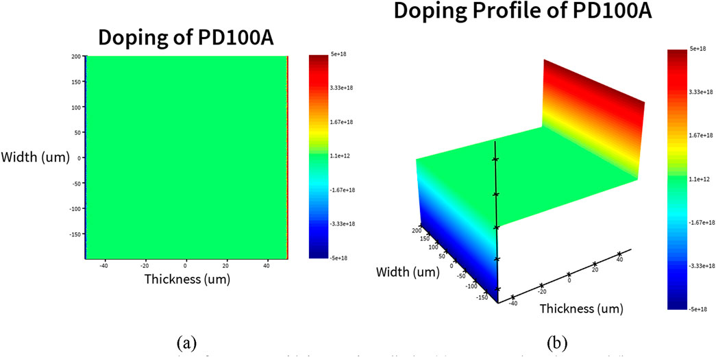
Figure 6. Doping distribution for 100 µm thickness photodiode: (a) cross-section view, and (b) angle view.
3.4 Simulation parameters
A sensitivity analysis was conducted by varying the thickness (100–400 μm) and area (0.16–10.24 mm2) while keeping other parameters constant, as summarized in Table 3. This approach demonstrates how changes in input variables (thickness or area) impact the output of the simulation (responsivity of the photodiodes).
Table 3. Key simulation parameters for silicon PIN PDs at 1064 nm.
4 Results and discussion
This section presents the responsivity versus dimensions for all three photodiode structures. The calculated responsivity values, estimated using Equations 5, 6, are compared with the simulated responsivity for each photodiode structure. Then, we analyze the light-trapping effects on responsivity and explore the optimal geometries for PDs with rear-side diffuse reflectors. Figure 7 illustrates how the optical path length in the PDs increases and how the light scatters due to the impacts of the rear-side diffuse reflectors on the incoming light and, subsequently, enhancing responsivity.
Figure 7. Optical simulation of the electrical generation rate (charge pairs/m3/s) in PD100A with various structures: (a) Structure 1, (b) Structure 2, (c) Structure 3, and (d) Structure 3 with side reflection.
4.1 Responsivity comparison of the photodiodes
Figure 8 compares the simulated responsivity of all three photodiode structures with values calculated using Equations 5, 6. For Structure 1 (no rear-side reflection), Figure 8a shows that simulated responsivity aligns closely with calculations from Equation 5, regardless of area variations. This agreement validates the simulation methodology and indicates that responsivity in Structure 1 depends primarily on thickness, with the area having a negligible impact. In addition, Figure 8b presents the responsivity for PDs with rear-side specular reflectors (Structure 2). The differences between the calculated responsivity (using Equation 6) and the simulated responsivity are minimal (<5%), even with varying photodiode areas. This validates the simulation approach and shows that the responsivity of PDs with specular reflectors depends mainly on thickness, not area. On the other hand, Figure 8c depicts the responsivity for PDs with rear-side diffuse reflectors (Structure 3). In this structure, the differences between the calculated and simulated responsivity are more significant due to the increased optical path length, which is influenced by both the area and thickness of the PDs. The maximum responsivity reaches up to 0.58 A/W, aligning with reported responsivities at 1064 nm for several PDs, as shown in Table 1 [16, 21, 43].
Figure 8. Simulated responsivity for: (a) PDs without rear-side reflector versus calculated responsivity using Equation 5, (b) PDs with specular reflector versus calculated responsivity using Equation 6, and (c) PDs with rear-side diffuse reflector versus calculated responsivity using Equation 6.
4.2 Optimal geometries for photodiodes with rear-side diffuse reflectors
Each of the 16 Si PIN PDs has been simulated in all three structures, and the responsivity values are compared in Figure 9a. The percentages of responsivity enhancement for PDs with diffuse reflectors (Structure 3) versus PDs without rear-side reflection (Structure 1) and with specular reflectors (Structure 2) are presented in Figure 9b.
Figure 9. Comparison of PDs with diffuse reflector vs PDs with specular reflector and PDs without reflector (a) Responsivity values, (b) Percentage of responsivity enhancement.
As seen in Figure 9a, the responsivity of PD200C, 200 µm thickness, with diffuse reflectors surpasses those of PDs with rear-side specular reflectors, 400 µm thickness (∼0.45 A/W vs. ∼0.43 A/W). Also, PD400D achieves the highest responsivity of 0.58 A/W at 1064 nm, slightly outperforming PD400C at 0.56 A/W and PD400B at 0.52 A/W. Put differently, expanding the area by 1600% (from ∼0.64 mm2 to ∼ 10.24 mm2) boosts responsivity by only ∼10%, an improvement outweighed by the resulting decline in electrical performance, notably increased dark current and NEP. Thus, the ceiling of the maximum achievable responsivity of Si PIN PDs at 1064 nm is ∼0.6 A/W as a result of using light trapping. On the other hand, Figure 9b shows that the enhancement in responsivity due to light trapping increases with larger areas but decreases with greater thickness. Thus, increasing the thickness enhances the responsivity, especially for larger PDs. However, the average responsivity enhancement diminishes to less than 10% when the thickness increases from 300 μm to 400 µm for PDs with diffuse reflectors, as shown in Figures 8c, 9b.
Overall, the dimensions of custom-made Si PIN PDs with light trapping should be chosen considering the optical and electrical characteristics trade-off to meet the desired responsivity without degrading the electrical characteristics. Also, the dimensions can be selected either to enhance responsivity while maintaining good electrical characteristics or to enhance electrical characteristics while maintaining good responsivity. For example, the photodiode PD300C, 300 µm thickness, and 2.56 mm2 area achieved a responsivity up to 0.53 A/W, surpassing state-of-the-art Si PIN PDs reported in the literature.
Another explored approach to optimize the performance of Si PIN PDs is to use side reflectors to maximize the responsivity with much smaller thicknesses and areas, which are favorable for better electrical characteristics. The benefits of the side reflector are maximized for small area PDs where the percentage of responsivity enhancement is ∼25% and 11% for 0.64 and 2.56 mm2 PDs, respectively, as shown in Figure 10. In our case, we used 50 µm SiO2 to reflect the light and maximize the optical path length without the necessity to enlarge the area of the PD elements. Filling the inter-element gaps in Si PIN PD elements in a photodetector array or quadrant with SiO2 prevents electrical crosstalk between adjacent photodiode elements, and it causes scattering or reflection of the light due to refractive index mismatch with silicon.
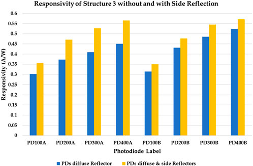
Figure 10. Responsivity comparison of Structure 3 PDs without and with side reflector.
5 Conclusion
In this work, we have investigated the impact of light trapping on the responsivity of silicon-based PIN PDs for light detection at 1064 nm. Thus, Ansys Lumerical FDTD and CHARGE have been utilized to simulate Si PIN PDs and obtain their optical and electrical characteristics versus varying dimensions. The following conclusions were obtained:
• When there are no diffuse reflectors, the optical characteristics, such as responsivity, of the simulated PIN PDs agree with the theoretical calculations and the reported values in the literature, as shown in Table 1.
• When there are diffuse reflectors, larger dimensions of the PDs lead to higher responsivity values, which agree with the reported results in Table 1. Results show that Si PIN PDs with rear-side diffuse reflectors significantly enhance responsivity, reaching up to 0.58 A/W for 400 µm thick PDs. However, additional methods should be investigated to be used alongside light trapping to enhance the responsivity up toward the maximum theoretical responsivity, 0.85 A/W, at 1064 nm.
• The light trapping increases responsivity values significantly in thin PIN PDs. For instance, thin PDs (100 µm thickness) with diffuse reflectors exhibit a higher responsivity (∼0.31 A/W) compared to thicker PDs (400 µm) without rear-side reflectors (∼0.28 A/W). However, the percentage of responsivity enhancement due to the light trapping decreases significantly in thicker PDs.
• There is a trade-off between the characteristics of optical and electrical properties. For instance, while PDs with the largest area and thickness showed the highest responsivity, they also exhibited the highest dark current and noise equivalent power, potentially limiting their utility in low-light or high-speed applications. Therefore, the optimal dimensions to realize high responsivity and low dark current (≤5 nA) are found to be 0.2–300 µm thickness and 0.6–2.5 mm2 area to form quadrant or array photodetectors.
• Filling the gaps between Si PIN photodiode elements with SiO2 can be used to optimize optical and electrical characteristics, such as achieving higher responsivity for smaller-size PD elements. Also, it provides electrical isolation, reducing electrical and optical crosstalk between adjacent elements.
• Simulations omit texturing side effects like high electric fields and interface defects, which could increase dark current (e.g., from 10 nA to 50 nA) and noise. Fabrication trials or advanced simulations (e.g., with defect modeling) are needed to quantify these impacts.
Data availability statement
The original contributions presented in the study are included in the article/supplementary material, further inquiries can be directed to the corresponding author.
Author contributions
FA: Conceptualization, Investigation, Methodology, Supervision, Validation, Writing–review and editing. NA: Conceptualization, Data curation, Formal Analysis, Methodology, Resources, Software, Validation, Writing–original draft. MA: Conceptualization, Data curation, Formal Analysis, Resources, Software, Validation, Writing–original draft, Writing–review and editing.
Funding
The author(s) declare that no financial support was received for the research and/or publication of this article.
Acknowledgments
The authors would like to express their sincere appreciation for the ongoing and invaluable support provided by King Abdulaziz City for Science and Technology (KACST).
Conflict of interest
The authors declare that the research was conducted in the absence of any commercial or financial relationships that could be construed as a potential conflict of interest.
Generative AI statement
The author(s) declare that no Gen AI was used in the creation of this manuscript.
Publisher’s note
All claims expressed in this article are solely those of the authors and do not necessarily represent those of their affiliated organizations, or those of the publisher, the editors and the reviewers. Any product that may be evaluated in this article, or claim that may be made by its manufacturer, is not guaranteed or endorsed by the publisher.
References
1. Penberthy WT, Vorwaller CE. Utilization of the 1064 Nm wavelength in photobiomodulation: a systematic review and meta-analysis. J Lasers Med Sci (2021) 12:e86. doi:10.34172/JLMS.2021.86
2. Yu X, Li Y, Gu X, Bao J, Yang H, Sun L. Laser-induced breakdown spectroscopy application in environmental monitoring of water quality: a review. Environ Monit Assess (2014) 186:8969–80. doi:10.1007/s10661-014-4058-1
3. Carp SA, Tamborini D, Mazumder D, Wu K-C, Robinson MR, Stephens KA, et al. Diffuse correlation spectroscopy measurements of blood flow using 1064 Nm light. J Biomed Opt (2020) 25:097003–15. doi:10.1117/1.jbo.25.9.097003
4. Affan Ahmed S, Mohsin M, Zubair Ali SM. Survey and technological analysis of laser and its defense applications. Defence Technology (2021) 17:583–92. doi:10.1016/j.dt.2020.02.012
5. Ma Y, Zhang Y, Gu Y, Shi Y, Chen X, Ji W, et al. Electron-initiated low noise 1064 Nm InGaAsP/InAlAs avalanche photodetectors. Opt Express (2018) 26:1028. doi:10.1364/oe.26.001028
6. Afzal AM, Dastgeer G, Iqbal MZ, Gautam P, Faisal MM. High-performance p-BP/n-PdSe2 near-infrared photodiodes with a fast and gate-tunable photoresponse. ACS Appl Mater Inter (2020) 12:19625–34. doi:10.1021/acsami.9b22898
7. Imran A, Sulaman M, Yang S, Bukhtiar A, Qasim M, Elshahat S, et al. Molecular beam epitaxy growth of high mobility InN film for high-performance broadband heterointerface photodetectors. Surf Inter (2022) 29:101772. doi:10.1016/j.surfin.2022.101772
8. Guan X, Yu X, Periyanagounder D, Benzigar MR, Huang JK, Lin CH, et al. Recent progress in short-to long-wave infrared photodetection using 2D materials and heterostructures. Adv Opt Mater (2021) 9:1–24. doi:10.1002/adom.202001708
9. Li Z, Chen C, Wang X, Zhang Y, Zhang H, Shen Z, et al. Photoelectric performance degradation of millisecond laser-irradiated silicon photodiodes. 2nd Int Symp Laser Interaction Matter (LIMIS 2012) (2013) 8796:87960R. doi:10.1117/12.2011267
10. Hicks C, Kalatsky M, Metzler RA, Goushcha AO. Quantum efficiency of silicon photodiodes in the near-infrared spectral range. Appl Opt (2003) 42:4415. doi:10.1364/ao.42.004415
11. Arshad TSM, Othman MA, Yasin NYM, Taib SN, Ismail MM, Napiah ZAFM, et al. Comparison on IV characteristics analysis between silicon and InGaAs PIN photodiode proc. Of 2013 3rd int. Conf. On instrumentation, communications, information technol., and biomedical engineering: science and technol. for improvement of health, safety, and environ. (2013) 70–5. doi:10.1109/ICICI-BME.2013.6698467
12. Eppeldauer GP, Larason TC, Houston JM, Vest RE, Arp U, Yoon HW. IR-enhanced Si reference detectors for one-step scale transfers from 300nm to 1000nm. Metrologia (2014) 51:S252–7. doi:10.1088/0026-1394/51/6/S252
13. Kaur H, Kaur HJ, Hooda MK, Gupta L. Electrical characteristics analysis of PIN detector with different doping concentration levels of N and P-type materials. Mater Today Proc (2020) 28:1879–86. doi:10.1016/j.matpr.2020.05.295
14. Wang K, Liu S, Li J, Wu S, Xia J, Chen J, et al. Enhancing the light absorptance of stain-etched black silicon decorated by TiN nanoparticles. J Mater Sci Mater Electronics (2021) 32:11503–10. doi:10.1007/s10854-021-05724-w
15. Guo X, Liu Q, Zhou H, Luan X, Li C, Hu Z, et al. High-responsivity Si photodiodes at 1060 Nm in standard CMOS technology. IEEE Electron Device Lett (2018) 39:228–31. doi:10.1109/LED.2017.2787147
16. Zhong H, Guo A, Guo G, Li W, Jiang Y. The enhanced light absorptance and device application of nanostructured black silicon fabricated by metal-assisted chemical etching. Nanoscale Res Lett (2016) 11:322. doi:10.1186/s11671-016-1528-0
17. Sakamoto A, Iida T, Yamamoto K, Kazuhisa Yamamura TN Semiconductor light-detecting element, 2 (2016).
18. Nguyen HT, Rougieux FE, Mitchell B, Macdonald D. Temperature dependence of the band-band absorption coefficient in crystalline silicon from photoluminescence. J Appl Phys (2014) 115. doi:10.1063/1.4862912
19. Photodiodes HS. Reduction of leakage current of large-area high-resistivity silicon p-i-n photodiodes for detection at 1.06 μm. IEEE Trans Electron Devices (1981) 28 (4) 412–416. doi:10.1109/t-ed.1981.20356
20. Zhong H, Ilyas N, Song Y, Li W, Jiang Y. Enhanced near-infrared absorber: two-step fabricated structured black silicon and its device application. Nanoscale Res Lett (2018) 13:316. doi:10.1186/s11671-018-2741-9
21. Hamamatsu. Si PIN photodiode for visible to infrared photometry (2024). Available online at: https://www.hamamatsu.com/eu/en/product/optical-sensors/photodiodes/si-photodiodes/S15137.html (accessed on June 11, 2024).
23. Korotcenkov G Porous silicon: from formation to applications: optoelectronics, microelectronics, and energy technology applications (2016).
24. Yamamoto K, Sakamoto A, Nagano T, Fukumitsu K. NIR sensitivity enhancement by laser treatment for Si detectors. Nucl Instrum Methods Phys Res A (2010) 624:520–3. doi:10.1016/j.nima.2010.03.128
25. Excelitas. Long wavelength enhanced silicon avalanche photodiodes (2024). Available online at: https://www.excelitas.com/product-category/yag-enhanced-photodiodes (accessed on June 11, 2024).
26. Osioptoelectronics 1064nm optimized photodetectors (2024). Available online at: https://www.osioptoelectronics.com/products/photodetectors/1064nm-nd-yag-photodiodes (accessed on 11 June 2024).
27. Hamamatsu. Hamamatsu photonics K.K., S.S.D. Technical note Si photodiodes (2024). Available online at: https://www.hamamatsu.com/content/dam/hamamatsu-photonics/sites/documents/99_SALES_LIBRARY/ssd/si_pd_kspd9001e.pdf (accessed on October 15, 2024).
28. Węgrzecki M, Piotrowski T, Puzewicz Z, Bar J, Czarnota R, Dobrowolski R, et al. New silicon photodiodes for detection of the 1064nm wavelength radiation. Electron Technology Conf (2016) 10175:101750Y. doi:10.1117/12.2257557
29. Li Z, Wang X, Shen Z, Lu J, Ni X. Numerical simulation of millisecond laser-induced damage in silicon-based positive-intrinsic-negative photodiode. Appl Opt (2012) 51:2759–66. doi:10.1364/AO.51.002759
30. Wang L, Luo H, Zuo H, Tao J, Yu Y, Yang X, et al. Highly sensitive narrowband Si photodetector with peak response at around 1060 nm. IEEE Trans Electron Devices (2020) 67:3211–4. doi:10.1109/TED.2020.3001245
31. Pelella A, Grillo A, Faella E, Luongo G, Askari MB, Di Bartolomeo A. Graphene-silicon device for visible and infrared photodetection. ACS Appl Mater Inter (2021) 13:47895–903. doi:10.1021/acsami.1c12050
32. Ahmad W, Ali MU, Laxmi V, Syed AS. Simulation and characterization of PIN photodiode for photonic applications. Asian J Nanoscience Mater (2018) 1:122–34.
33. Scagliotti M, Salvato M, De Crescenzi M, Boscardin M, Castrucci P. Influence of the contact geometry on single-walled carbon nanotube/Si photodetector response. Appl Nanoscience (Switzerland) (2018) 8:1053–8. doi:10.1007/s13204-018-0720-1
34. Park KS, Yoon YS, Park JM, Kang JY, Kim BW, Hwang IG, et al. Estimates of the photo-response characteristics of a non-fully-depleted silicon p-i-n photodiode for the near infrared spectral range and the experimental results. J Korean Phys Soc (2007). 50:1156–62. doi:10.3938/jkps.50.1156
35. Alsolami A, Hussain H, Noor R, AlAdi N, Almalki N, Kurdi A, et al. Recent advances in black silicon surface modification for enhanced light trapping in photodetectors. Appl Sci (Switzerland) (2024). 14:9841. doi:10.3390/app14219841
36. Tang Q, Shen H, Yao H, Jiang Y, Li Y, Zhang L, et al. Formation mechanism of inverted pyramid from sub-micro to micro scale on c-Si surface by metal assisted chemical etching temperature. Appl Surf Sci (2018). 455:283–94. doi:10.1016/j.apsusc.2018.05.023
37. Lumerical. Optoelectronic modeling (2012). Available online at: https://www.lumerical.com/learn/whitepapers/optoelectronic-modeling/(accessed on June 20, 2024).
38. Optics ansys. ANSYS germanium-on-silicon lateral photodetector (2024). Available online at: https://optics.ansys.com/hc/en-us/articles/360042828913-Germanium-on-Silicon-lateral-photodetector (accessed on March 5, 2025).
39. Ansys. Ansys Canada ltd PML boundary conditions in FDTD and MODE (2024). Available online at: https://optics.ansys.com/hc/en-us/articles/360034382674-PML-boundary-conditions-in-FDTD-and-MODE (accessed on June 20, 2024).
40. ANSYS Selecting the Best Mesh Refinement Option in the FDTD Simulation Object (2024). Available online at: https://optics.ansys.com/hc/en-us/articles/360034382614-Selecting-the-best-mesh-refinement-option-in-the-FDTD-simulation-object (accessed on March 7, 2025).
41. ANSYS Understanding the Non-Uniform Mesh in FDTD (2024). Available online at: https://optics.ansys.com/hc/en-us/articles/360034382634-Understanding-the-non-uniform-mesh-in-FDTD (accessed on March 12, 2025).
42. Fan Z, Cui D, Zhang Z, Zhao Z, Chen H, Fan Y, et al. Recent progress of black silicon: from fabrications to applications. Nanomaterials (2021) 11:41–26. doi:10.3390/nano11010041
43. Zhao JH, Li XB, Chen QD, Chen ZG, Sun HB. Ultrafast laser-induced black silicon, from micro-nanostructuring, infrared absorption mechanism, to high performance detecting devices. Mater Today Nano (2020) 11:100078. doi:10.1016/j.mtnano.2020.100078
44. Zhao Z, Zhang Z, Jing J, Gao R, Liao Z, Zhang W, et al. Black silicon for near-infrared and ultraviolet photodetection: a review. APL Mater (2023) 11. doi:10.1063/5.0133770
45. Zhao S, Yuan G, Wang Q, Liu W, Wang R, Yang S. Quasi-hydrophilic black silicon photocathodes with inverted pyramid arrays for enhanced hydrogen generation. Nanoscale (2020) 12:316–25. doi:10.1039/c9nr06635g
Keywords: silicon PIN photodiode, responsivity, near-infrared light, black silicon, light trapping, numerical simulation
Citation: Alghannam F, Alharthi NS and Alayed M (2025) Enhancing responsivity of silicon PIN photodiodes at 1064 nm via light trapping and geometry optimization: a simulation study. Front. Phys. 13:1563838. doi: 10.3389/fphy.2025.1563838
Received: 20 January 2025; Accepted: 20 March 2025;
Published: 11 April 2025.
Edited by:
Lu Liu, Harbin Engineering University, ChinaReviewed by:
Kun Liao, Peking University, ChinaWei Ren, Xi’an University of Posts and Telecommunications, China
Copyright © 2025 Alghannam, Alharthi and Alayed. This is an open-access article distributed under the terms of the Creative Commons Attribution License (CC BY). The use, distribution or reproduction in other forums is permitted, provided the original author(s) and the copyright owner(s) are credited and that the original publication in this journal is cited, in accordance with accepted academic practice. No use, distribution or reproduction is permitted which does not comply with these terms.
*Correspondence: Mrwan Alayed, bWFsYXllZEBrYWNzdC5lZHUuc2E=