 Ahmed Fathi Salem1,2
 Mohamed Farhat. O. Hameed
3,4*
Mohamed Farhat. O. Hameed
3,4*
 Hamdy Abdelhamid
5*Sanaa M. El-Rabaie1
Hamdy Abdelhamid
5*Sanaa M. El-Rabaie1
 S. S. A. Obayya
2,4*R. El-Bashar6
S. S. A. Obayya
2,4*R. El-Bashar6
- 1 Physics and Engineering Mathematics Department, Faculty of Electronic Engineering, Menoufia University, Menouf, Egypt
- 2 Centre for Photonics and Smart Materials, Zewail City of Science, Technology and Innovation, Giza, Egypt
- 3 Center for Nanotechnology, Zewail City of Science, Technology and Innovation, Giza, Egypt
- 4 Faculty of Engineering, University of Mansoura, Mansoura, Egypt
- 5 Electrical Engineering Department, College of Engineering and Information Technology, Ajman University, Ajman, United Arab Emirates
- 6 National Institute of Laser Enhanced Sciences (NILES), Cairo University, Giza, Egypt
The development of wide-bandgap perovskite materials has enabled new opportunities for highly efficient tandem solar cell applications. In this study, the optical and electronic performance of a single junction dome-shaped nanostructured wide-bandgap perovskite (MA0.9Cs0.1Pb(I0.6Br0.4)3) is studied for all-perovskite tandem solar cell (SC) applications. The optical performance of the proposed design is studied using finite difference time domain. The introduction of the dome-shaped (Al2O3) antireflective layer improves the light absorption to 90.1% relative to 77.1% for the PSC without antireflective coating (ARC). Therefore, the maximum power conversion efficiency (PCE) of 15.3% is reported for the optimized structure (Eg = 1.82 eV) with an enhancement of 19.5% compared to the reference cell. When the defect density is increased to 1018 cm-3, the PCE is dropped to 7.7% with a reduction of 49.7% relative to the studied good practical defect density of 1015 cm-3. Furthermore, the impact of the perovskite bandgap on the electrical parameters of the perovskite solar cells (PSCs) device is analyzed. The optimized structure with a bandgap of 1.9 eV shows the highest PCE of 16.1% with a JSC of 18.1 mA/cm2. The results show that the presence of Al2O3 ARC enhances the performance of PSC, which can be useful for tuning wide-bandgap perovskite in tandem photovoltaic systems.
1 Introduction
The photovoltaic effect is used by solar cells (SCs) to transform light energy into electrical energy. Solar cells are generally categorized into different generations based on the underlying technology used in their fabrication [1–3]. Because of their superior stability and high conversion efficiencies, crystalline silicon solar cells (the first generation of photovoltaic technology) control over 90% of the PV market, making them the most popular photovoltaic devices [4]. Their high production costs and intricate construction procedure, however, restrict their applicability for a range of uses. Second-generation solar cells were fabricated by cheaper technologies compared to the first-generation solar cells [5] Nevertheless, they failed to achieve the efficiencies of first-generation solar cells. The benefits of first- and second-generation PVs are combined in third-generation devices. The most popular types of third-generation photovoltaics include dye-sensitized solar cells (DSSCs), organic solar cells (OSCs), quantum dot solar cells (Qdot SCs), and perovskite solar cells (PSCs) [1, 6, 7]. PSCs are considered to be of special importance owing to their ability to convert visible light into electricity efficiently [8–10]. Therefore, in this research, we will focus on currently emerging perovskite-based solar cell technology.
The growing attention toward halide perovskite (HP) solar cells has grown significantly because of their higher power conversion efficiency. Single junction PSCs’ PCE has increased from 3.8% to 25.2% in just over 10 years [11, 12]. In this structure, the A-site is occupied by a monovalent cation (e.g., methylammonium, MA), the B-site by a metal cation (e.g., lead, Pb), and the X-site by a halide anion (e.g., iodine, I). Accordingly, halide perovskites (HPs) follow the general chemical formula ABX3. Typically, HPs have high absorption coefficients, large carrier diffusion lengths, high carrier mobilities, and tunable bandgaps [8–10, 13]. Moreover, perovskite thin-film SCs offer unique advantages over traditional semiconductor thin-film SCs, such as solution processability and mechanical flexibility [14, 15]. Nevertheless, monovalent cation perovskites such as MAPbI3 suffer from instability [2]. Therefore, organic–inorganic mixed-cation and mixed-halide perovskite compounds were developed to mitigate stability issues [16]. Mixed-cation and mixed-halide perovskite MAxCs1-xPb(IxBr1-x)3 is gaining a lot of attention due to its higher bandgap and consequently higher voltage, stability, and broad-spectrum absorption [17]. MAxCs1-xPb(IxBr1-x)3 thin film was developed to increase the chemical stability of the light-absorbing material without the additional encapsulation [18]. In this regard, Chang et al. [18] fabricated an efficient and stable MA0.8Cs0.2Pb(I0.8Br0.2)3 thin film SC, which results in a power conversion efficiency (PCE) of 10.0% with short circuit current (JSC) of 14.15 mA/cm2. Further, MAxCs1-xPb(IxBr1-x)3 is a suitable top sub-cell to develop a multijunction SC. In this respect, Rajagopal et al. [19] fabricated perovskite/perovskite tandem solar cell with MA0.9Cs0.1Pb(I0.6Br0.4)3 and MAPb0.5Sn0.5I3 as a top and bottom cell absorber material, respectively. The authors achieved an interesting PCE of 18.5%.
Enhancing light trapping and absorption in thin absorber layers requires extending the photon propagation path length beyond the traditional Lambertian limit [20]. To achieve this, plasmonic nanostructures have been integrated into solar cells, utilizing near-field enhancement and efficient light scattering to boost optical absorption [21–23]. Furthermore, nanowire architectures have emerged as promising alternatives to thin-film solar cells, offering superior performance while significantly reducing material consumption [23–25]. In this concern, Mohammadi et. al [23]. employed three-dimensional simulations to investigate the light-trapping effects of plasmonic core/shell nanorod arrays on PSC performance. By optimizing nanorod geometry and materials-specifically using Ag cores with CuSCN shells—the device achieved enhanced absorption and carrier generation, resulting in a PCE of 19.33% with a JSC of 23.12 mA/cm2 and VOC of 1 V. Furthermore, antireflection attached to front side of the glass substrate can improve the optical transmittance [22, 24] and light tapping inside the active material. Further, Wu et al. [22] found that incorporating irregularly shaped silver nanomaterials into the electron transport layer of PSC can enhance both light trapping and carrier extraction through combined far-field scattering and near-field plasmonic effects. This strategy improved device performance significantly, increasing the PCE from 19.52% to 22.42%. Despite these advances, reflection losses at the air–top electrode interface remain a major challenge, as they reduce the amount of light reaching the active layer. Therefore, achieving effective index matching at this interface is crucial during the device design process. This can be realized by introducing textured antireflective coatings (ARCs), which enable a gradual refractive index transition from the transparent electrode to air [26–29]. In this regard, Tavakoli et al. [29] show that the nanocone-based array antireflection film can enhance the optical transmittance and introduce superhydrophobicity, improving the PCE from 12.1% to 13.14%. In 2021, Shahiduzzaman et al. [26] proved that incorporating a nanostructured ARC significantly boosts light coupling, improving the top subcell’s JSC from 20.5 mA/cm2 (without ARC) to 23.6 mA/cm2 (with textured ARC). Furthermore, a PSC structure with an Al2O3 pyramid anti-reflection layer was proposed by Liu et al. [28]. The authors found that the textured Al2O3 ARC can contribute to photon management in PSCs through improved light coupling. Compared with the flat PSC, the efficiency of the PSC with an Al2O3 ARC increased from 14.01% to 17.19%. A combination of back-reflector nanostructures and surface gratings resulted in enhanced absorption in thin-film Si solar cells [27]. The absorption can be improved for shorter wavelengths via antireflection effects of surface grating, whereas the longer wavelengths are enhanced through plasmon interactions of the back-reflector nanostructures. Lately, Chen et al. [30] introduced a UV-resistant sticker-type nanostructured acrylic resin antireflective film to enhance the light-trapping and stability of PSCs, reducing average reflectance by 4.06% and increasing PCE from 20.77% to 22.1%. Additionally, the resin antireflective film demonstrated excellent durability under prolonged UV exposure and was successfully applied to large-area CIGS solar cells, highlighting its potential for commercial photovoltaic applications.
The ARC has a significant effect on both the top and the bottom sub-cells of tandem solar cells. It minimizes the front-surface Fresnel losses, allowing more light to enter the tandem stack and couple effectively into the wide-bandgap perovskite top cell. This not only boosts absorption in the top cell but also helps more light reach the bottom cell. For the 2-Terminal (2-T) tandem SCs, the ARC boosts the photon absorption in the top cell at shorter wavelengths. Additionally, it allows more longer-based wavelengths to reach and be absorbed by the bottom cell as well. Further, the ARC can be optimized to enhance the JSC and decrease the current mismatch between the two sub-cells [31]. Shahiduzzaman et al. [26] demonstrated that adding a nanostructured MgF2 ARC significantly enhances light coupling in both the top and bottom cell. At shorter wavelengths (around 550 nm), more photons are absorbed in the top cell, while at longer wavelengths (around 730 nm), the photons penetrate deeper and are absorbed by both cells, resulting in a noticeable increase in absorption within the bottom cell. In contrast, for 4-terminal (4-T) tandem solar cells, the overall conversion efficiency is simply the sum of the independently measured efficiencies of the two sub-cells. Unlike 2-T tandem cells, there is no current-matching requirement between the sub-cells. Therefore, increasing the JSC of the top cell using an ARC is beneficial; however, it does not influence the performance of the bottom sub-cell.
In this work, we examine the optical and electronic performance of a single-junction dome-shaped nanostructured wide-bandgap perovskite solar cell, focusing on the MA0.9Cs0.1Pb(I0.6Br0.4)3 composition, which is suitable for tandem architectures. The mixed-cation, mixed-halide MAxCs1-xPb(IxBr1-x)3 thin film was developed to address stability issues [17]. Therefore, MA0.9Cs0.1Pb(I0.6Br0.4)3, possessing a band gap of 1.82 eV, is selected in this study. Furthermore, this specific composition is chosen since experimental optical data are available. Different textured AR designs using MgF2 and Al2O3 layers are proposed to enhance light management and overall device efficiency. The optoelectronic performance of the suggested PSC structure is evaluated using the SILVACO TCAD. In this regard, the FDTD is initially employed for a precise investigation of the optical simulation. Electrical simulation depends on the finite element method (FEM), in which the Poisson and drift-diffusion equations are computed, considering both bulk and interface recombination mechanisms. In this research, incorporating dome-shaped (Al2O3) antireflective structures led to a significant enhancement in light absorption, increasing it to 90.1% compared to 77.1% for the PSC without ARC. This improvement in optical performance translated to a PCE of 15.3%, representing an enhancement of 19.5% over the conventional structure without ARC. The PCE dropped to 7.7% when the defect density was increased to 1018 cm-3, which represents a 49.7% decrease in comparison to the practical defect density of 1015 cm-3. These results provide important novel insights for designing nanostructured wide-bandgap perovskites that will improve efficiency in tandem photovoltaic applications.
2 Design considerations and simulation methodology
The 3D schematic diagram for the suggested PSC configuration with the dome-shaped nanostructure is shown in Figure 1. As depicted in Figure 1, the proposed architecture consists of multiple functional layers, including the MgF2 AR coating, transparent conducting oxide (ITO), hole transport layer (NiO), active perovskite absorber (MA0.9Cs0.1Pb(I0.6Br0.4)3), electron transport layer (C60), and metallic electrode (Ag). In this regard, the studied unit cell in 3D is shown in a gray dashed line. Figure 1b presents the perovskite solar cell (PSC) structure featuring a dome-shaped antireflective (AR) grating, simulated using the SILVACO tool (DevEdit) in the X–Y plane. The dome-shaped geometry is defined by the period (p), the dome height (h1), and the bottom AR layer thickness (h2), with the dome height measured from the top of the grating structure. The simulation domain for optical modeling is depicted in Figure 1c. To analyze the impact of this dome-shaped AR structure on light management and device performance, electromagnetic interactions are examined using the FDTD method, which is integrated with the ATLAS device simulation tool for a comprehensive electro-optical assessment. To minimize computational cost, the simulation considers a single unit cell along the x-axis, using periodic boundary conditions (PBCs), while perfectly matched layers (PMLs) are applied along the positive y-axis. A perfect electric conductor (PEC) is used along the negative y-axis to represent the back metallic reflector, which blocks light transmission. In this work, the absorption edge is set at 680 nm, aligning with the bandgap of MA0.9Cs0.1Pb(I0.6Br0.4)3, which is approximately 1.82 eV [19]. Simulations are performed by applying a normal-incidence plane wave under AM1.5G conditions, with an input power density of 0.1 W/cm2 to represent standard one-sun illumination. The J–V characteristics are analyzed using the AM1.5G spectrum data provided by the National Renewable Energy Laboratory (NREL) [32]. The perovskite absorber is initially set to a thickness of 190 nm [19], with the hole and electron transport layers (HTL and ETL) fixed at 30 nm and 50 nm, respectively [19]. The complex optical refractive indices of all layers are sourced from existing literature [19]. Considering realistic conditions such as resistance paths, reflection at the front contact (ITO), and various recombination mechanisms, including Shockley-Read-Hall (SRH), radiative, and Auger recombination. Carrier mobility concentration dependence and bandgap narrowing (BGN) effects are also considered [33, 34]. A summary of the electrical parameters for the different layers is provided in Table 1, as well as the work functions of the ITO and Ag electrodes, as 4.3 eV and 5.0 eV, respectively [19]. This design approach and simulation framework enable a rigorous evaluation of the optical and electronic performance enhancements achieved through the dome-shaped AR structure. In this work, both optical and electrical simulations are employed to study the performance of the reported PSC device. In optical simulation, the finite-difference time-domain (FDTD) method is employed to calculate the generation rate (Equation 1), which is used as an input for the electrical simulation. Furthermore, electrical simulation in ATLAS is based on the numerical solution of basic equations of charge transport, including Poisson’s equation, the continuity equations, and transport equations [35, 36]. These fundamental equations were solved on the finite element mesh (FEM) grid points, allowing the calculation of the current density of electrons and holes, and the current density–voltage (J−V) characteristic of the photovoltaic cell. Figure 2 depicts a flowchart summarizing the optical and electrical simulation steps in SILVACO TCAD, along with the principal equations solved in the ATLAS device simulator. The utilized materials are defined by the complex refractive index of each layer and illuminated under the AM1.5G spectrum. In this regard, the optical input is modeled using FDTD to calculate the spatial generation rate. This generation profile is then coupled into the ATLAS device simulator, where continuity, Poisson, and transport equations are solved to describe carrier dynamics, recombination, and electrostatics. The combined method enables precise prediction of photovoltaic performance, yielding key outputs such as J–V characteristics and EQE. The photogeneration rate is given by:
where |E| 2 is the electric field intensity, η is the quantum yield, defined as the fraction of absorbed photons that are converted to photogenerated electron-hole pairs, ℎ is Planck’s constant, λ is the wavelength, c is the speed of light, and α is the absorption coefficient. To analyze and evaluate the optical performance in the context of photovoltaic performance, an average weighted absorption to the AM1.5G solar spectrum [37]. Solar weighted average absorption (Aav) and reflection (Rav) can be calculated from Equations 2, 3, respectively:
where λg is the cut-off wavelength corresponding to the band gap of the perovskite material utilized. I(λ) is the solar irradiance at AM1.5G [32, 38].

Figure 1. (a) Schematic diagram of perovskite solar cell structure with a grated antireflective layer, and (b) Cross-sectional simulation model with PML and periodic boundary conditions. (c) Geometrical parameters of the grating unit cell.

Table 1. The electrical parameters of the simulated structure used in the PSC.
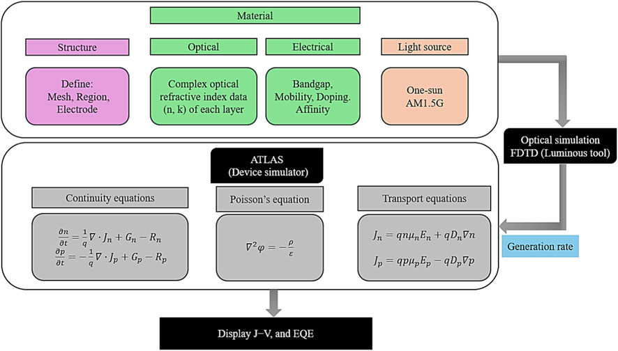
Figure 2. A flowchart of optical and electrical simulation.
The power conversion efficiency (PCE) can be calculated as given by Equation 4 using [2],
where Pi is the average solar power density (∼100 mW/cm2), and Po is the output PSC power density. FF is the fill factor, and JSC here takes the recombination effects into account. FF quantifies how closely the device’s performance approaches the ideal product of VOC and JSC [39].
3 Results and discussion
3.1 Model validation and initial study
Initially, the wide-bandgap MA0.9Cs0.1Pb(I0.6Br0.4)3 PSC without the proposed AR surface [19] is analyzed to validate the simulation framework used in this study. In this respect, the structural schematic diagram established in SILVACO Atlas is shown in Figure 3a, which consists of an ITO front contact, NiO hole transport layer (HTL), the mixed-halide wide-bandgap perovskite absorber (MA0.9Cs0.1Pb(I0.6Br0.4)3), C60 electron transport layer (ETL), and an Ag back electrode. Further, the energy-level alignment of the PSC layers is shown in Figure 3b, highlighting the conduction and valence band positions and illustrating the built-in potential that drives carrier separation and extraction. Figure 3c shows the J–V simulation results of the suggested model compared to the experimental results. The close agreement between the simulation (blue circles) and experimental data (red line) highlights the accuracy of the model. This consistency confirms the reliability of the chosen optical and electrical parameters, including defect states, recombination mechanisms, and carrier mobility models. Table 2 shows the electrical parameters of the studied PSC versus the data provided for the published experimental work [19]. Similarly, Figure 3d shows the external quantum efficiency (EQE) spectrum, where the simulated curve closely matches the experimentally measured data. The excellent correspondence between the simulated and experimental results across both J–V and EQE measurements validates the accuracy of the simulation methodology. This provides confidence in extending the validated simulation approach to explore and optimize advanced device architectures, such as the proposed dome-shaped antireflective structures PSC design.

Figure 3. (a) The structural schematic diagram, (b) energy-level band diagram of PSC, (c) Current density–voltage (J–V) curve and (d) external quantum efficiency (EQE) of the planar PSC structure compared with experimental data [19].

Table 2. The short-circuit current density (JSC), open-circuit voltage (VOC), filling factor (FF) and power conversion efficiency (PCE) of the simulated and experimental PSC.
Figure 4 provides a comparative analysis of the considered PSC structure with the suggested dome-shaped (MgF2) versus the conventional planar ARC layer and without ARC. The periodicity is set at 400 nm, and the total ARC thickness of the surface dome-shaped is fixed at 500 nm (h1 = 300 nm, h2 = 200 nm) for a fair comparison as in Figure 4b. In this regard, absorption spectra, EQE and the corresponding J–V behavior are presented in Figures 4a,c,d, respectively. One can notice that the absorption spectra of the structure with ARC are nearly enhanced over the corresponding solar spectrum of the studied PSC, attributed to improved light coupling and reduced reflection losses. The average optical efficiency of the studied PSC with the flat ARC is enhanced to 81.3% versus 77.1% without using the ARC layer. With using the surface dome-shaped ARC layer, the optical efficiency is elevated to 83.8% with an enhancement of 3.1% and 8.6% versus the structure with and without using the planar ARC. Figure 3b shows that the dome-shaped ARC consistently enhances EQE compared to both the planar ARC and no-ARC structures. With taking the electrical parameters into consideration, we notice that the suggested PSC structure offers the highest J–V characteristic, further confirming the performance gains offered by the dome-shaped surface AR layer. The short circuit current density (JSC) and the corresponding PCE for the dome-shaped design are increased to 16.7 mA/cm2 and 13.8%, respectively, relative to 16.3 mA/cm2 and 13.4% for the structure with a planar ARC, and 15.6 mA/cm2 and 12.8% for the structure without the ARC. Overall, these results confirm that integrating the dome-shaped ARC grating enhances light harvesting and carrier collection, leading to significant performance improvements in the PSC structure-demonstrating the effectiveness of the dome-shaped design in addressing optical limitations compared to planar configurations.
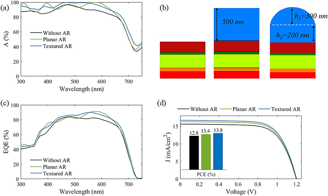
Figure 4. (b) The studied PSC schematic structures with and without the suggested planar and dome-shaped ARC (MgF2) at period of 400 nm, the corresponding (a) absorption spectra, (c) EQE and the (d) J–V curve and PCE.
3.2 Influence of the antireflective coating parameters
Figure 5 illustrates the contour plot of the JSC of the suggested PSC with an MgF2 anti-reflection coating as a function of the period (P) and height (h). Specifically, the graph shows how JSC varies as a function of the grating period (p) for three different dome heights (h1 = 300 nm, 400 nm, and 500 nm), while keeping the ARC base layer thickness (h2) constant at 200 nm. The color bar minimum corresponding to the JSC the conventional flat ARC structure studied. Across all cases, the textured ARC demonstrates superior performance to the flat structure. With the configuration using h1 = 500 nm (i.e., h2 = zero) at periodicity of 600 nm, the offered dome-shaped nanostructure yields the highest current densities, exceeding 16.8 mA/cm2. The observed performance enhancement results are due to the increased light coupling and reduced reflectance owing to the dome-shaped texture. This structure effectively increases light trapping and thus the photon absorption within the perovskite layer [26]. Light scattering is strongest when structural dimensions match the incident wavelength. Given that the solar spectrum’s center wavelength is near 600 nm, surfaces structured with a 600 nm period achieve maximum optical absorption [40]. As a result, JSC peaks at a 600 nm period, which is therefore consistently adopted for the structured surface design in this study. These findings emphasize the critical importance of precisely adjusting the ARC dome’s height and periodicity to optimize light harvesting and enhance the photovoltaic performance of wide-bandgap PSCs.
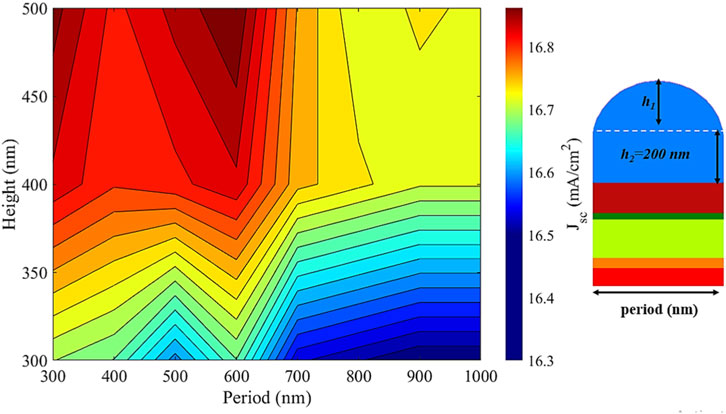
Figure 5. The short circuit current density of PSC as a function of period (p) and height (h1) of textured MgF2 ARC.
The MgF2 has a low refractive index (∼1.38), traditionally suitable for air/glass interfaces. However, its index is slightly high compared to the top ITO contact layer utilized. Generally, for typical ITO films, the refractive index is in the range of 1.6–2.2 [41]. Comparatively, Al2O3 has a higher refractive index of ∼1.75 at 632 nm [42, 43], which may provide a better refractive index gradient in nanostructured or textured geometries when transitioning from air to the underlying ITO layer [41, 44]. In this respect, a comparative study is performed using Al2O3 as an alternative ARC material. Figure 6 presents a comparative study between MgF2 and Al2O3 as dome-shaped antireflective coatings in the optimized PSC architecture. After identifying the ideal geometry for the textured ARC, these two dielectric materials were evaluated for their optical and electrical performance enhancements.
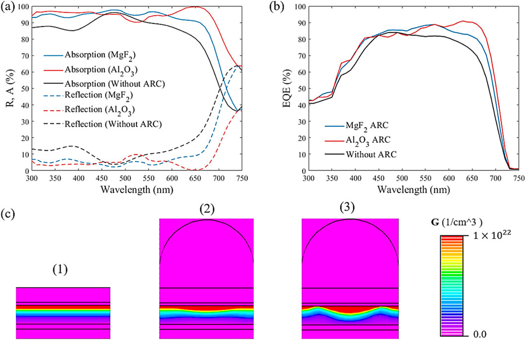
Figure 6. (a) Absorption and reflection spectra, and (b) EQE of the proposed dome-shaped design using MgF2 and Al2O3 ARC relative to reference PSC. (c) Generation profile for 1) PSC without ARC, 2) PSC with MgF2 ARC, and 3) PSC with Al2O3 ARC.
Figure 6 displays the absorption (A) and reflection (R) spectra of the PSCs equipped with MgF2 (blue) and Al2O3 (red) suggested domes. It is evident that the Al2O3-coated PSC exhibits higher broadband light absorption, especially from 600 to 700 nm. Therefore, a significant reduction in reflection losses compared to MgF2 is observed at the aforementioned range from 600 to 700 nm as shown in Figure 6a. This enhanced light-coupling is attributed to the low refractive index contrast between nanostructured dome-shaped Al2O3 and air, providing a better impedance match at the front interface. Furthermore, the enhanced light-coupling due to the small refractive index difference between the Al2O3 layer and top ITO contact layer air, provides a better impedance match at the front interface. The ITO acts as an intermediate optical medium between the ARC and the perovskite absorber (∼2.5–2.7). Therefore, the use of a higher-index ARC such as Al2O3 contributes to reduced reflectance and improved light in-coupling in the interested wavelength range from 600 nm to 700 nm. Although the absorption spectrum is reduced from the wavelength of 450–580 nm, the photogenerated carriers is improved. The average absorption (Aaᵥ) and reflection (Raᵥ) over the considered spectral range are shown in Table 3. The Al2O3-based structure shows an average absorption of 91.1%, significantly higher than 84.2% for MgF2. Conversely, the average reflection is reduced from 15.8% (MgF2) to 8.9% (Al2O3), confirming the superior antireflective performance of the Al2O3 coating. Figure 5b presents the external quantum efficiency (EQE) of the two configurations, where the Al2O3-coated PSC consistently outperforms Al2O3, particularly in the 600–700 nm wavelength range, indicating better photo-generated carrier collection due to improved light harvesting. This performance boost arises not only from the overall enhancement in optical absorption but also because it covers the solar spectrum’s peak photon flux at nearly 670 nm [45].

Table 3. The Average absorption (Aav) and reflection (Rav) of the studied dome-shaped design using MgF2 relative to Al2O3 ARC.
The ARC plays a crucial role in suppressing PSC reflection and increasing the light absorption [46]. The ARC affects the light coupling and reflectance through its refractive index and thickness. This depends on decreasing the refractive index mismatch between air and the device with better light coupling and reduced Fresnel reflection. When the ARC refractive index with quarter-wave thickness is properly chosen, reflectance will be minimized [47]. This will increase the light coupling into the absorber with improved device performance. However, this occurs at a certain wavelength. To increase the absorption wavelength range, grading structures have been widely used [2, 48, 49]. Figure 6a and (b) illustrates the absorption and reflection spectra for the PSC without ARC, PSCs with a dome-shaped MgF2, and Al2O3 ARCs structures. It may be seen that the PSC with ARC has a small reflection spectrum with broadband higher light absorption compared to the reference cell. Further, the overall light absorption is improved using the high refractive index Al2O3 relative to the MgF2 one. To better understand this behavior, the generation rate profiles of all the studied structures are examined. Figure 6c compares the generation profiles for the three studied cases. It is evident that the ARC significantly increases the generation rate intensity relative to the flat PSC. Further, Figure 6c(3) shows that the PSC with the high-index ARC (Al2O3) exhibits a higher generation rate than the PSC with the lower-index ARC Figure 6c(2). This improvement results not only from the top-index grating, which enhances light coupling from air, but also from the refractive index of Al2O3 being closer to that of the underlying ITO. As a result, the impedance mismatch is reduced, enabling more efficient light coupling into the ITO layer. Consequently, the high-index Al2O3 ARC facilitates deeper light penetration and enhances absorption within the PSC.”
Figure 7a illustrates the output electrical power density as a function of voltage for the studied designs. The dome-shaped with MgF2 reference structure achieves a JSC of 16.9 mA/cm2 and a PCE of 13.9%. In contrast, the nanostructure with suggested Al2O3 material attains enhanced performance, with a JSC of 17.5 mA/cm2 and an efficiency of 14.5%, as shown in Figure 7b. This improvement is attributed to the dome-shaped structure which provides a smoother refractive index transition between air and the device surface, resulting in better optical impedance matching. In addition, the close refractive index of Al2O3 and the ITO layer provide a better light coupling to the perovskite material, followed by the ITO layer. These findings highlight the effectiveness of the dome-shaped grating based on the Al2O3 nanostructure material in enabling high-efficiency solar cell designs. These improvements are in line with recent reports demonstrating the effectiveness of high-index AR layers like Al2O3 in minimizing optical losses and boosting photovoltaic performance [50, 51].
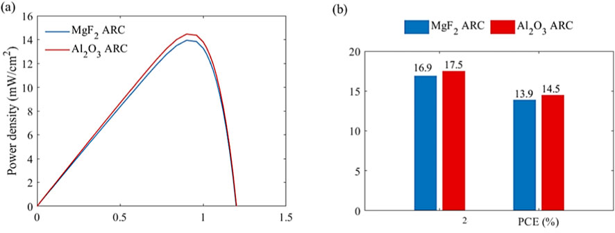
Figure 7. (a) Power density-voltage characteristics of the suggested dome-shaped and (b) the corresponding JSC and PCE for the MgF2 and the Al2O3 ARC materials of the PSC.
3.3 Influence of absorber layer thickness
The thickness of the active layer is responsible for controlling the diffusion length and, consequently, the carrier lifetime of the charge carriers [52]. Therefore, in this study, we investigate the thickness-dependent performance of the wide-bandgap (WBG) perovskite system MA0.9Cs0.1Pb(I0.6Br0.4)3. As shown in Figure 8a, the JSC increases with active layer thickness due to enhanced light absorption, particularly within the visible spectrum, but reaches saturation beyond approximately 450 nm, in accordance with the Beer–Lambert Absorbance law [53]. For WBG perovskites [17], with bandgaps in the range of 1.8–2.0 eV that primarily absorb higher-energy photons, thinner layers (∼200–400 nm) are sufficient to maximize JSC. With the increase of the active layer thickness up to 250 nm, the light absorption and thus the current density is improved, and therefore the open-circuit voltage (VOC) is slightly improved to 1.2 V [54]. The inherently higher VOC of WBG perovskites (theoretically ∼1.2–1.5 V) remains advantageous for tandem integration [55]. If the thickness is further increased, the VOC exhibits a slight decline, as in Figure 8b, as a result of the bulk recombination increase and the reduced electric field strength [2].
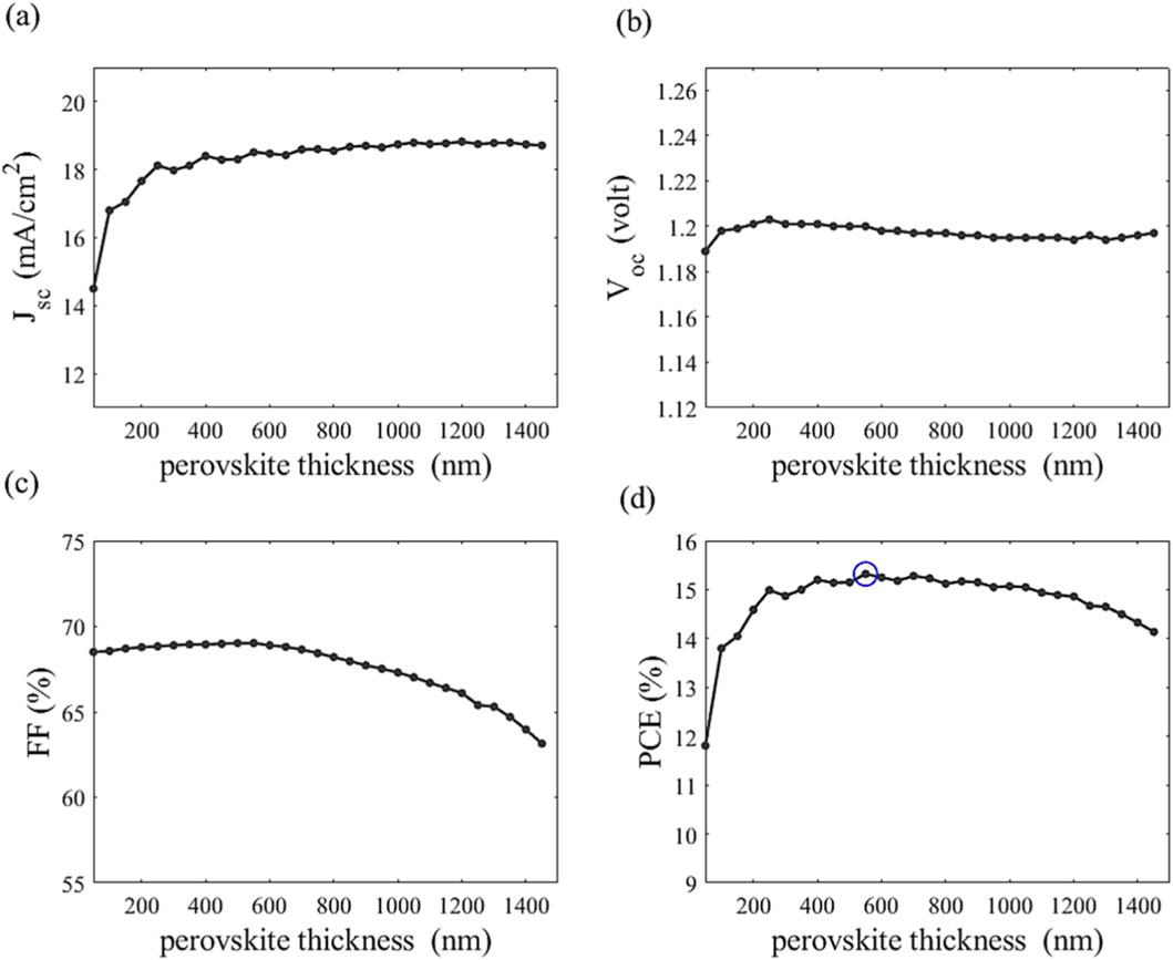
Figure 8. Variation of (a) JSC (b) VOC and (c) FF and (d) PCE versus the active layer thickness for PSC with Al2O3 ARC.
The fill factor is an important metric for figuring out PSCs’ conversion efficacy. Charge transport rates compete with recombination rates, making it essential to minimize recombination to enable efficient carrier extraction and maintain a high fill factor (FF). Lower than the thickness of 500 nm, we observe that the charge transport is good, compatible with the VOC curve behavior. When the thickness is increased above this value, the charge transport is highly affected by the recombination-based thickness. FF deteriorates, as in Figure 8c, due to increased series resistance and carrier recombination, although the superior charge-carrier mobility in WBG perovskites may partially offset these losses, provided interfacial defects such as halide segregation are effectively passivated [56]. Figure 8d shows the corresponding PCE versus the active material thickness from 300 nm to 1400 nm. The maximum PCE of 15.3% can be obtained at the active material thickness of 550 nm. Such a value represents an optimal trade-off between the JSC, VOC, and FF of 18.5 mA/cm2, 1.2 V, and 69%, respectively, for working as an optimum single junction solar cell. In contrast, within tandem cell architectures, precise tuning of the wide-bandgap (WBG) perovskite thickness is essential to maximize overall efficiency while ensuring spectral current matching with the bottom subcell [57]. If the thickness is increased to 1400 nm, the PCE is slightly lessened to 14.1%. Notably, the mixed-cation (Cs/MA) and mixed-halide (I/Br) composition in this WBG system offers improved phase stability compared to MAPbI3, reducing defect densities and enhancing operational durability. Overall, these findings highlight the critical role of thickness optimization, nanostructuring, in advancing high-performance WBG perovskite subcells for efficient tandem solar cell architectures.
To understand the growth behavior of the JSC with the cell thickness, the light absorption spectrum and the corresponding EQE are studied for the proposed PSC as presented in Figure 9. In this study, optoelectronic behaviors are shown at different thicknesses from 50 nm followed by the optimum thickness of 550 nm to a large thickness of 1400 nm. The absorption spectra (Figure 9a) demonstrate a clear thickness-dependent behavior, exhibiting significantly enhanced light absorption across the visible spectrum (400–700 nm) due to increased photon capture. In particular, the 700 nm-thick device exhibits an absorption spectrum nearly identical to that of the 550 nm-thick optimal device, which is consistent with the intrinsically high absorption coefficients of perovskite materials. The average absorption of the thickness of 700 nm is equal to 90.7% relative to 90.1% for the 550 nm-thick value. This means that the active material absorbs nearly all the light penetrated for the spectrum range higher than its bandgap. The average absorption of the suggested PSC at different device thicknesses is presented in Table 4. If the thickness is decreased to 200 nm and 50 nm, the absorption of low photon energy is reduced. Therefore, the average absorption is reduced to 87.8% for the cell thickness of 50 nm, with a reduction of 2.6% versus the absorption-based optimum thickness. If the thickness is further increased to 1000 nm and 1400 nm, the average absorption is increased to 92.7% and 95.7% for the width of 1000 nm and 1400 nm, respectively, with an enhancement of 2.9% and 6% against the optimum thickness absorption. This is owing to the increase in the path length, which enhances the absorption spectra for wavelengths above 700 nm, as shown in Figure 9a.
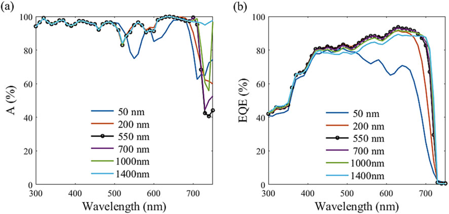
Figure 9. (a) Total absorption spectra and (b) EQE of PSC for PSC with Al2O3 ARC.

Table 4. Average light absorption of the offered PSC device with different active layer thicknesses.
Figure 9b shows the corresponding EQE for the offered dome-shaped PSC with the different active layer thicknesses. The reduced blue response is primarily due to surface recombination at the front interface. In contrast, the diminished red response is attributed not only to rear surface recombination but also to the limited carrier diffusion length and the weaker absorption of longer wavelengths [58]. Interestingly, the EQE of the ultrathin 50 nm layer declines sharply beyond 500 nm wavelength, underscoring the trade-off between optical absorption and carrier collection efficiency in thin films. This may be attributed to the insufficient thickness of the absorber layer, dominating the diffusion current relative to the depletion region drift current [59]. If the active layer is too thin to establish a robust drift field or if recombination dominates, the overall collection (including drift) can be poor. Moreover, the light absorption is located near the electrodes, thus the carriers are likely recombined at the electrode’s surfaces [3]. At a wavelength of 670 nm, the peak solar photon flux wavelength [45], as a reference, the EQE drops to approximately 61% at this wavelength. In contrast, the EQE spectra (Figure 9b) reflect similar increase trends, with a thicker active layer till the 700 nm-thick value. This may be attributed to the small defect density of 1015 cm-3, making it not effective at the EQE (i.e., the short circuit current) test [2]. At the thicknesses of 550 nm and 700 nm, the EQE is saturated at nearly 93% at the wavelength of 670 nm. If the thickness is further increased to 1400 nm, the average absorption still increases to 95.7%. However, we notice that their corresponding EQEs above 400 nm start decreasing, affected by the studied defect density of 1016 cm-3. The corresponding EQE is decreased to approximately 87% at the reference wavelength.
To figure out the light-trapping effect involved in the proposed structure, Figure 10 depicts the electric field (E-field) profiles of the PSC with textured ARC at a period of 600 nm (Figures 10a–c) and 300 nm (Figures 10d–f). E-field profiles are shown for monochromatic illumination of 300 nm, 550 nm, and 700 nm. For short wavelengths of 300 nm, most of the incident light is absorbed by the ARC (Al2O3) and ETL (TiO2), and only a small fraction of light is absorbed by the perovskite layers as shown in Figures 10a,d. For the wavelength of 550 nm, the incident light is effectively absorbed by the absorber and does not interact with the back contact as illustrated in Figures 10b,e. As the incident light wavelength increased to 700 nm, the incident photons having higher energies reached the rear contact to form a standing wave in the active layer. Figure 10c, f) shows the electric field distributions for the wavelength of 700 nm at periods of 300 nm and 600 nm, respectively. For the case of 300 nm period, where the period is smaller than the wavelength, a standing wave is formed, without diffraction, in the active layer as shown in Figure 10f. On the other hand, the incident light is diffracted at a period of 600 nm, as depicted in Figure 10c, since the period is comparable to the incident wavelength of 700 nm [2, 60]. Additionally, the separation between successive maxima is calculated by
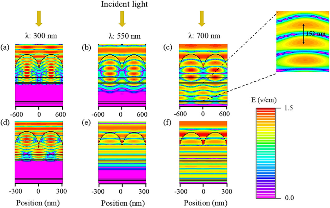
Figure 10. Electric field profiles of the suggested PSC with Al2O3 ARC for an incident wavelength of (a,d) 300 nm, (b,e) 550 nm, and (c,f) 700 nm, respectively. The absorber layer has a thickness of 550 nm.
3.4 Influence of defect density of the absorber
In this respect, the proposed studies integrate defect density analysis with the J–V characteristics, as shown in Figure 11. One can notice that the JSC remains relatively constant at approximately 18.5 mA/cm2 for defect densities below 1016 cm-3, suggesting efficient carrier collection in low-defect films. However, the JSC declines markedly at higher defect concentrations, indicating that bulk recombination becomes dominant beyond this critical threshold [54]. The PCE shown in Figure 11b exhibits a similar behavior of the JSC. When the defect density is increased to 1 × 1017 cm-3 and 1 × 1018 cm-3, the PCE is dropped to from 15.3% to 14.6% and 7.7%, respectively, highlighting the detrimental influence of defects on overall device performance. Figure 11c shows that the VOC is nearly constant under 1016 and slightly decreases to 1.19 at the defect density of 1 × 1019 cm-3. Further, Figure 11c displays heightened sensitivity of the fill factor (FF) and open-circuit voltage (VOC) to defect density. Specifically, the FF decreases significantly from approximately 69%–42.2% as the defect density increases from 1016 to 1018 cm-3. This reflects intensified defect-assisted non-radiative recombination, which limits charge extraction efficiency and consequently reduces both JSC and PCE [54, 62]. These trends are further validated by the J–V curves in Figure 11d, where higher defect densities manifest as reduced JSC, VOC, FF, and thus the PCE due to increased recombination losses. The electrical output of the proposed PSC at different defect densities is shown in Table 5. At the defect density of 1018 |1019 cm-3, the PCE dropped to 2.6% and 1.8%, with a reduction of 83.0% | 88.2% relative to the good defect density of 1016 cm-3, due to the decrease of the JSC and FF to 15 mA/cm2 |4.6 mA/cm2 and 42.2% |33.1%, respectively. Even though the Al2O3 ARC efficiently increases light coupling and reduces optical losses, under high-defect scenarios, its optical advantages are negated by significant electrical losses. These results highlight how crucial it is to use defect suppression approaches to maintain high PCEs in PSCs [63], such as compositional engineering, interfacial passivation, or perovskite crystallization optimization.

Figure 11. Variation of (a) JSC (b) PCE and (c) FF and VOC versus the defect density and (d) J–V curve at different defect densities for PSC with Al2O3 ARC.
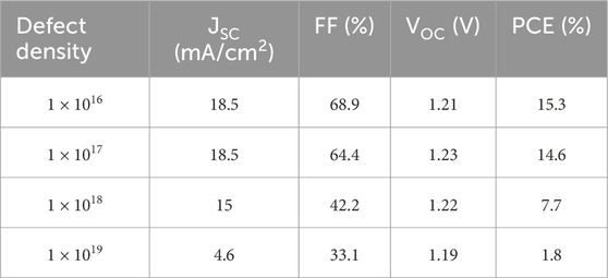
Table 5. The electric results of the proposed PSC device at different defect densities.
3.5 Influence of the absorber bandgap
The bandgap of the absorber layer is a very crucial parameter in solar cell design. Therefore, the effect of the bandgap of MA0.9Cs0.1Pb(IxBr1-x)3 on the electrical parameters is investigated. Zang et al. [64] succeeded in fine-tuning the bandgap by reducing the [Br] content from 1 to 0, corresponding to an absorption spectrum edge tweaked from red to green. In this regard, the optoelectronic characteristic of the suggested design is investigated by tuning the bandgap from 1.53 to 2.24 eV [64]. This study is operated while maintaining the other layers’ parameters at the values listed in Table 1. The extinction coefficient curves of different bandgaps are achieved by fitting the reference k-curve with an Urbach tail [65] at the corresponding cut-off wavelength, as shown in Figure 12. In this study, the extinction coefficient k(λ) of the proposed MA0.9Cs0.1Pb(I0.6Br0.4)3 with bandgap of 1.82 eV is used as a reference. The extinction coefficient was modeled with an exponential Urbach tail from the absorption edge to analyze the absorption tail variation with cut-off wavelength. The absorber layer bandgap effect on the electrical solar cell performance is depicted in Figure 13. Consistent with the average absorption trend shown in Figure 12, the JSC attains its maximum value at lower bandgaps and declines markedly with increasing the bandgap, as illustrated in Figure 13a. On the other hand, the VOC increases due to the increase of the material bandgap as presented in Figure 13b. The results show that the FF (Figure 13c) is increased from 26% to 79% with the increase of the bandgap from 1.53 to 1.9. Therefore, the PCE is improved from 12.1% to a maximum value of 16.1% as visualized in Figure 13d. If the bandgap is further increased above 1.9, the FF and therefore PCE are decreased to 42% and 5% at the bandgap of 2.24, respectively. In this regard, the optimal bandgap value at 1.9 eV yields a PCE of 16.1%, FF of 67.8%, VOC of 1.32 V, and JSC of 18.1 mA/cm2.
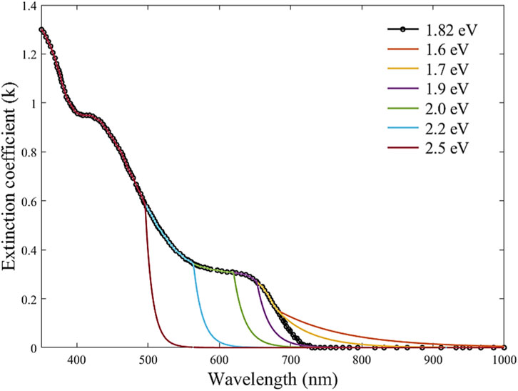
Figure 12. Extinction coefficient for different bandgaps.
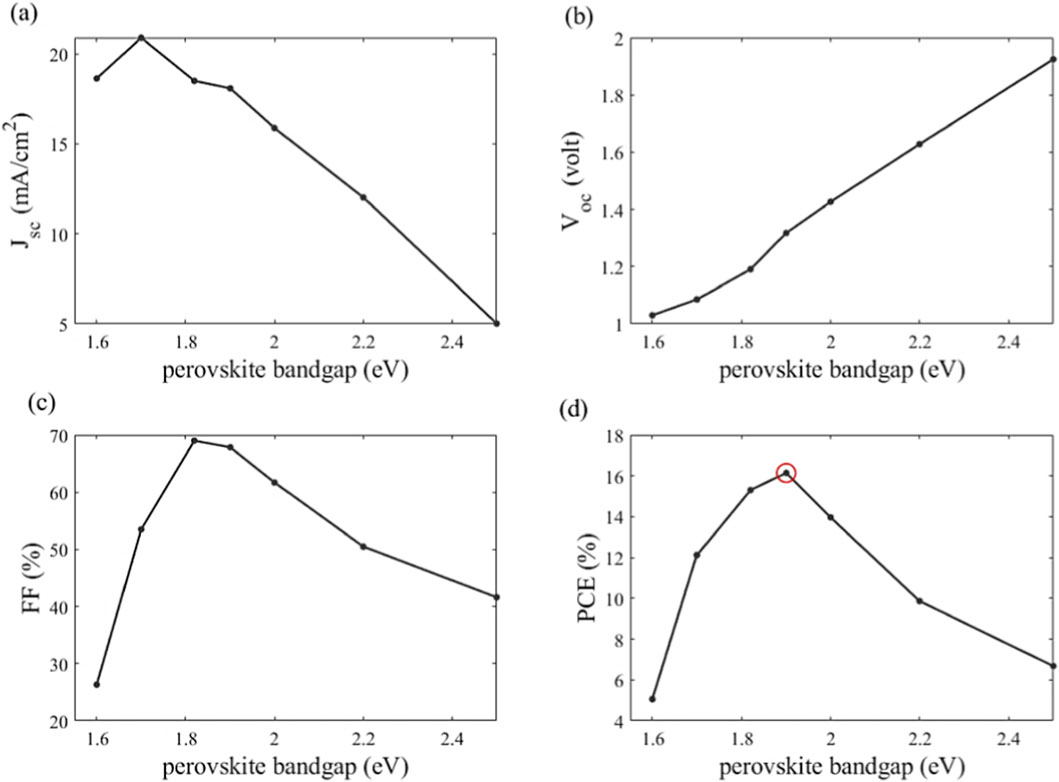
Figure 13. Variation of (a) JSC (b) VOC and (c) FF and (d) PCE versus the bandgap for PSC with Al2O3 ARC.
Table 6 compares the performance of WBG PSCs with various compositions. It is observed that MA0.9Cs0.1Pb(I0.6Br0.4)3 PSC exhibits a relatively lower JSC compared to other PSCs listed in Table 6; however, it delivers a high VOC of 1.21 V. In addition, the MA-based wide-bandgap perovskite exhibits a stable phase compared to FA-based mixed-halide systems, which usually show a portion of the yellow phase when exposed to ambient conditions [66, 67]. Matondo et al. [67] developed Cesium–Methylammonium (CsMA)–based perovskite solar cells with large grain size, less grain boundaries, and high crystallinity, especially in MA0.9Cs0.1Pb(I0.6Br0.4)3 films. It can be seen that the extracted JSC from the (FAPbI3)0.85(MAPbBr3)0.2 perovskite is higher than that of the reported MA0.9Cs0.1Pb(I0.6Br0.4)3 cell. This enhancement can be attributed to its relatively low band gap value of 1.67 eV, which enables absorption of a wider portion of the solar spectrum and thus offers a higher JSC.
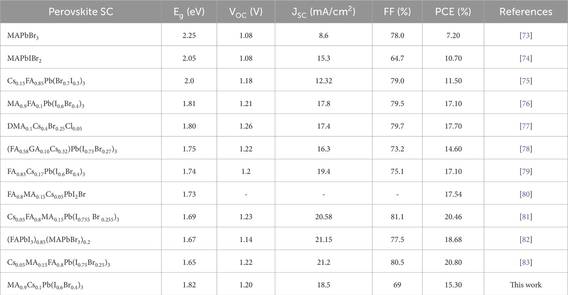
Table 6. A comparison between the reported WBG organic–inorganic PSC and those reported previously in the literature.
4 Suggested fabrication methodology
The proposed device fabrication is assumed to begin with the precise deposition of a 55 nm ITO thin film onto a glass substrate, serving as the transparent conductive electrode. A NiOx (30 nm) precursor solution is then spin-coated onto the cleaned ITO surface. Subsequently, the (550 nm) perovskite precursor solution was spin-coated using a two-step spin program. After film formation, a C60 (50 nm) layer is thermally evaporated onto the perovskite. Finally, a 150 nm-thick silver (Ag) electrode is deposited under high vacuum as the rear contact [19]. The fabrication of the textured antireflective coating (ARC) is achieved by casting a nanostructured film onto a patterned silicon master using advanced semiconductor processing techniques [26, 68]. UV Nanoimprint Lithography (UV-NIL) technique can be introduced to fabricate nanostructured Al2O3 as reported in [68]. Nanoimprint lithography (NIL) has various advantages such as large area coverage, high throughput, and a cost-effective patterning process [68–70]. Additionally, NIL is a simple and fast process for forming nanostructures [68]. Figure 14 depicts a schematic diagram of the process steps for the fabrication of nanostructured Al2O3 using a Polydimethylsiloxane (PDMS) mold. Initially, nanostructured Si master stamps are utilized to transfer the nanostructure pattern to the PDMS mold (Figure 14a). After preparing the resin and mold, the Al2O3 dispersion resin is left on the PDMS mold. Then, spin-coating is performed at 3000 rpm for 30 s (Figure 14b). After spin coating, the substrate is covered on a resin-coated PDMS mold (Figure 14c). To ensure uniform transfer, a pressure of 5 bar is applied while the PDMS mold and substrate are exposed to UV light (365 nm, 4500 mW/cm2) for 20 min (Figure 14d). During this step, the Al2O3 resin is cured to form the nanostructures on the glass substrate. Finally, the PDMS mold is slowly detached from the Al2O3 nanostructure (Figure 14e). At the end of the above process, textured Al2O3 ARC is well formed on the glass substrate.
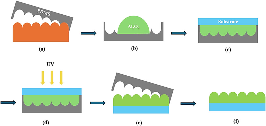
Figure 14. Schematic diagram of the suggested fabrication process of the Al2O3 nanostructure by UV-NIL. (a) Demolding (b) drop the Al2O3 and spin coating (c) put down a on spin-coated PDMS (d) exposure UV and press (e) detach the PDMS (f) Al2O3 pattern.
5 Conclusion
In summary, we have demonstrated that integrating a dome-shaped antireflective nanostructure into a wide-bandgap MA0.9Cs0.1Pb(I0.6Br0.4)3 perovskite absorber markedly enhances light harvesting and device performance. Compared to a PSC without ARC, the textured Al2O3 ARC with optimized thickness boosts the optical absorption from 77.1% to 90.1%, with a peak PCE of 15.3% and an improvement of 19.5% over the initial flat design. Furthermore, we investigated the effect of defect density in the absorber layer. We found that increasing the defect density to 1018 cm-3 reduces the PCE to 7.7%. However, low defect densities (<1016 cm-3) maintain high efficiency, underscoring the critical importance of precise materials and interface engineering. The impact of the perovskite bandgap on the PSC is also investigated. The best efficiency of 16.1% is achieved with a bandgap of 1.9 eV. These results not only validate the effectiveness of dome-shaped AR architectures for maximizing photon utilization in wide-bandgap perovskites but also provide clear guidelines on thickness, geometry, and defect control for their deployment in high-efficiency tandem solar cells. Future work will focus on experimental realization, long-term stability testing, and the integration of these nanostructures into full tandem modules to fully leverage their potential in next-generation photovoltaics.
Data availability statement
The original contributions presented in the study are included in the article/supplementary material, further inquiries can be directed to the corresponding authors.
Author contributions
AS: Conceptualization, Formal Analysis, Methodology, Validation, Writing – original draft. MH: Conceptualization, Formal Analysis, Project administration, Resources, Supervision, Writing – review and editing. HA: Project administration, Resources, Writing – review and editing, Funding acquisition. SE-R: Writing – review and editing. SO: Writing – review and editing, Conceptualization, Formal Analysis, Project administration, Resources, Supervision. RE-B: Conceptualization, Formal Analysis, Investigation, Supervision, Writing – review and editing.
Funding
The author(s) declared that financial support was received for this work and/or its publication. This work is partially funded by Ajman University, UAE, Project number: 2024-IRG-ENIT-18. The authors also acknowledge the Foreign Expert Project of Ministry of Human Resources and Social Security (H20251011), China.
Conflict of interest
The author(s) declared that this work was conducted in the absence of any commercial or financial relationships that could be construed as a potential conflict of interest.
The reviewer MZ declared a past co-authorship with the author(s) HA, SO to the handling editor.
Generative AI statement
The author(s) declared that generative AI was not used in the creation of this manuscript.
Any alternative text (alt text) provided alongside figures in this article has been generated by Frontiers with the support of artificial intelligence and reasonable efforts have been made to ensure accuracy, including review by the authors wherever possible. If you identify any issues, please contact us.
Publisher’s note
All claims expressed in this article are solely those of the authors and do not necessarily represent those of their affiliated organizations, or those of the publisher, the editors and the reviewers. Any product that may be evaluated in this article, or claim that may be made by its manufacturer, is not guaranteed or endorsed by the publisher.
References
1. Shah N, Shah AA, Leung PK, Khan S, Sun K, Zhu X, et al. A review of third generation solar cells. Processes (2023) 11(6):1852. doi:10.3390/pr11061852
2. Salem AF, El-Bashar R, El-Rabaie SM, Abdelhamid H, Hameed MFO, Obayya SSA. Nanoscale grating-based perovskite solar cell with improved efficiency. Phys Scr (2024) 99(11):115504. doi:10.1088/1402-4896/ad7dc1
3. El-Bashar R, Hussein M, Hegazy SF, Badr Y, Rahman BMA, V Grattan KT, et al. Electrical performance of efficient quad-crescent-shaped Si nanowire solar cell. Sci Rep (2022) 12(1):48. doi:10.1038/s41598-021-03597-x
4. Sopian K, Cheow SL, Zaidi SH. An overview of crystalline silicon solar cell technology: past, present, and future, AIP Conf Proc 1877 1, 020004. Melville, NY: AIP Publishing LLC (2017). doi:10.1063/1.4999854
5. Schmid M. Revisiting the definition of solar cell generations. Adv Opt Mater (2023) 11(20):2300697. doi:10.1002/adom.202300697
6. Eswaramoorthy N, Syamsai R, Nallusamy S, Pitchaiya S, Venkatraman MR. Recent progress of carbonaceous materials in third generation solar cells: DSSCs. Handbook Porous Carbon Mater (2023) 165–88. doi:10.1007/978-981-19-7188-4_7
7. Li F, Liu K, Dai J. Flexible pin perovskite solar cell with optimized performance by KBF4 additive. Opt Express (2023) 32(1):366–78. doi:10.1364/OE.503856
8. Absorber OTP. Electron-hole diffusion lengths exceeding 1 micrometer in an. Science (2013) 342(6156):341–344. doi:10.1126/science.1243982
9. Qin P, Tanaka S, Ito S, Tetreault N, Manabe K, Nishino H, et al. Inorganic hole conductor-based lead halide perovskite solar cells with 12.4% conversion efficiency. Nat Commun (2014) 5(1):3834. doi:10.1038/ncomms4834
10. Patel PK. Device simulation of highly efficient eco-friendly CH3NH3SnI3 perovskite solar cell. Sci Rep (2021) 11(1):3082. doi:10.1038/s41598-021-82817-w
11. Kojima A, Teshima K, Shirai Y, Miyasaka T. Organometal halide perovskites as visible-light sensitizers for photovoltaic cells. J Am Chem Soc (2009) 131(17):6050–1. doi:10.1021/ja809598r
12. Green MA, Dunlop ED, Hohl-Ebinger J, Yoshita M, Kopidakis N, Hao X. Solar cell efficiency tables (version 56). Prog Photovoltaics: Res Appl (2020) 28(7):629–38. doi:10.1002/pip.3303
13. Duan C, Zhang X, Du Z, Chen J, El-Bashar R, Obayya SSA, et al. Perovskite interface defect passivation with poly (ethylene oxide) for improving power conversion efficiency of the inverted solar cells. Opt Express (2023) 31(12):20364–76. doi:10.1364/OE.489290
14. Bi C, Chen B, Wei H, DeLuca S, Huang J. Efficient flexible solar cell based on composition-tailored hybrid perovskite. Adv Mater (2017) 29(30):1605900. doi:10.1002/adma.201605900
15. Yang D, Yang R, Ren X, Zhu X, Yang Z, Li C, et al. Hysteresis-suppressed high-efficiency flexible perovskite solar cells using solid-state ionic-liquids for effective electron transport. Adv Mater (2016) 28(26):5206–13. doi:10.1002/adma.201600446
16. Imani R, Borca CH, Pazoki M, Edvinsson T. Excited-state charge polarization and electronic structure of mixed-cation halide perovskites: the role of mixed inorganic–organic cations in CsFAPbI 3. RSC Adv (2022) 12(39):25415–23. doi:10.1039/d2ra04513c
17. Marwaha S. Numerical analysis to investigate the influence of various HTLs on MA 0.9 Cs 0.1 Pb (I 0.6 Br 0.4) 3 based perovskite solar cells. In: 2024 international conference on intelligent systems and advanced applications (ICISAA). IEEE (2024) 1–6.
18. Chang SH, Tseng P-C, Chiang S-E, Wu J-R, Chen Y-T, Chen C-J, et al. Structural, optical and excitonic properties of MAxCs1-xPb (IxBr1-x) 3 alloy thin films and their application in solar cells. Solar Energy Mater Solar Cells (2020) 210:110478. doi:10.1016/j.solmat.2020.110478
19. Rajagopal A, Yang Z, Jo SB, Braly IL, Liang P, Hillhouse HW, et al. Highly efficient perovskite–perovskite tandem solar cells reaching 80% of the theoretical limit in photovoltage. Adv Materials (2017) 29(34):1702140. doi:10.1002/adma.201702140
20. Han SE, Chen G. Toward the Lambertian limit of light trapping in thin nanostructured silicon solar cells. Nano Lett (2010) 10(11):4692–6. doi:10.1021/nl1029804
21. Zhang Q, Zhao M, Li Y, Bian A, El-Bashar R, Abdelhamid H, et al. Polarization dependent exciton-plasmon coupling in PEA2PbI4/Al and its application to perovskite solar cell. Opt Express (2024) 32(14):25327–42. doi:10.1364/OE.529605
22. Wu Y, Sun X, Dai S, Li M, Zheng L, Wen Q, et al. Broad-band-enhanced plasmonic perovskite solar cells with irregular silver nanomaterials. ACS Appl Mater Inter (2022) 14(14):16269–78. doi:10.1021/acsami.2c01759
23. Mohammadi MH, Fathi D, Eskandari M. Light trapping in perovskite solar cells with plasmonic core/shell nanorod array: a numerical study. Energy Rep (2021) 7:1404–15. doi:10.1016/j.egyr.2021.02.071
24. El-Bashar R, Eissa A, Hameed MFO, Abdelhamid H, Obayya SSA. Diamond-shaped nanowires solar cell for light absorption enhancement. 2025 42nd Natl Radio Sci Conf (Nrsc) (2025) 1:229–35. doi:10.1109/nrsc65659.2025.11018536
25. El-Bashar R, Hussein M, Hegazy SF, Badr Y, Hameed MFO, Obayya SSA. Efficient silicon nanowires solar cell. In: 2021 international applied computational electromagnetics society symposium (ACES). IEEE (2021) 1–2.
26. Shahiduzzaman M, Hossain MI, Visal S, Kaneko T, Qarony W, Umezu S, et al. Spray pyrolyzed TiO 2 embedded multi-layer front contact design for high-efficiency perovskite solar cells. Nanomicro Lett (2021) 13:1–17. doi:10.1007/s40820-020-00559-2
27. Lin H-Y, Kuo Y, Liao C-Y, Yang CC, Kiang Y-W. Surface plasmon effects in the absorption enhancements of amorphous silicon solar cells with periodical metal nanowall and nanopillar structures. Opt Express (2012) 20(S1):A104–A118. doi:10.1364/oe.20.00a104
28. Liu L, Liu W, Fu W, Yi Z, Yi Y, Zhang J, et al. Enhancing the overall performance of perovskite solar cells with a nano-pyramid anti-reflective layer, Photonics (2024) 11 8:715. doi:10.3390/photonics11080715
29. Tavakoli MM, Tsui K-H, Zhang Q, He J, Yao Y, Li D, et al. Highly efficient flexible perovskite solar cells with antireflection and self-cleaning nanostructures. ACS Nano (2015) 9(10):10287–95. doi:10.1021/acsnano.5b04284
30. Chen B, Yao D, Dong P, He J, Su J, Ma B, et al. UV-Resistant nanostructured anti-reflective film for achieving efficiency enhancement of perovskite solar cells and potential of fabricating large-scale Cu (in, Ga) Se2 solar cells. ACS Appl Mater Inter (2025) 17(6):9266–77. doi:10.1021/acsami.4c18588
31. Zhao Y, Datta K, Phung N, Bracesco AEA, Zardetto V, Paggiaro G, et al. Optical simulation-aided design and engineering of monolithic perovskite/silicon tandem solar cells. ACS Appl Energy Mater (2023) 6(10):5217–29. doi:10.1021/acsaem.3c00136
32. Air Mass 1.5 Solar Spectra. National Renewable Energy Laboratory (NREL). Available online at: https://www.nrel.gov/grid/solar-resource/spectra-am1.5.html (Accessed December 23, 2025).
33. Hima A, Lakhdar N, Benhaoua B, Saadoune A, Kemerchou I, Rogti F. An optimized perovskite solar cell designs for high conversion efficiency. Superlattices Microstruct (2019) 129:240–6. doi:10.1016/j.spmi.2019.04.007
34. Boukortt NEI, Patanè S, AlAmri AM, AlAjmi D, Bulayyan K, AlMutairi N. Numerical investigation of perovskite and u-CIGS based tandem solar cells using silvaco TCAD simulation. Silicon (2023) 15(1):293–303. doi:10.1007/s12633-022-01960-9
35. Fakhri N, Salay Naderi M, Gholami Farkoush S, SaeidNahaei S, Park S-N, Rhee S-B. Simulation of perovskite solar cells optimized by the inverse planar method in SILVACO: 3D electrical and optical models. Energies (Basel) (2021) 14(18):5944. doi:10.3390/en14185944
36. Silvaco International (2004). ATLAS User’s Manual: Device simulation software (PDF). Available online at: https://www.eng.buffalo.edu/∼wie/silvaco/atlas_user_manual.pdf.
37. Spence M, Hammond R, Pockett A, Wei Z, Johnson A, Watson T, et al. A comparison of different textured and non-textured anti-reflective coatings for planar monolithic silicon-perovskite tandem solar cells. ACS Appl Energy Mater (2022) 5(5):5974–82. doi:10.1021/acsaem.2c00361
38. Standard solar spectra | PVEducation. Available online at: https://www.pveducation.org/pvcdrom/appendices/standard-solar-spectra (Accessed December 23, 2025).
39. El-Broullesy SM, El-Bashar R, Ramadan MRI, Aboul-Enein S, Ibrahim A, Wood DH, et al. Broadband absorption of modified conical nanowires for photovoltaic applications. Optik (Stuttg) (2022) 271:170245. doi:10.1016/j.ijleo.2022.170245
40. Zhang Y, Xuan Y. Comprehensive design of omnidirectional high-performance perovskite solar cells. Sci Rep (2016) 6(1):29705. doi:10.1038/srep29705
41. Refractive index of In2O3-SnO2 (indium tin oxide, ITO) - konig. Available online at: https://refractiveindex.info/?shelf=other&book=In2O3-SnO2&page=Konig (Accessed December 23, 2025).
42. Hendriks W, Dijkstra M, van Emmerik CI, Hegeman I, García-Blanco SM. High refractive index low-loss aluminium oxide waveguides. In: Eur. Conf. Integr. Opt. (2020) 1 2–4.
43. Malitson IH, Dodge MJ. Refractive index and birefringence of synthetic sapphire. J Opt Soc Am (1972) 62(11):1405.
44. Konig TAF, Ledin PA, Kerszulis J, Mahmoud MA, El-Sayed MA, Reynolds JR, et al. Electrically tunable plasmonic behavior of nanocube–polymer nanomaterials induced by a redox-active electrochromic polymer. ACS Nano (2014) 8(6):6182–92. doi:10.1021/nn501601e
45. Kumar P, You S, Vomiero A. Recent progress in materials and device design for semitransparent photovoltaic technologies. Adv Energy Mater (2023) 13(39):2301555. doi:10.1002/aenm.202301555
46. Seo K-H, Biswas S, Eun J, Kim H, Bae J-H. Numerical study on overcoming the light-harvesting limitation of lead-free Cs2AgBiBr6 double perovskite solar cell using moth-eye broadband antireflection layer. Nanomaterials (2023) 13(23):2991. doi:10.3390/nano13232991
47. Kim K-H, Park Q-H. Perfect anti-reflection from first principles. Sci Rep (2013) 3(1):1062. doi:10.1038/srep01062
48. Qarony W, Hossain MI, Dewan R, Fischer S, Meyer-Rochow VB, Salleo A, et al. Approaching perfect light incoupling in perovskite and silicon thin film solar cells by moth eye surface textures. Adv Theor Simul (2018) 1(8):1800030. doi:10.1002/adts.201800030
49. Hossain MI, Hongsingthong A, Qarony W, Sichanugrist P, Konagai M, Salleo A, et al. Optics of perovskite solar cell front contacts. ACS Appl Mater Inter (2019) 11(16):14693–701. doi:10.1021/acsami.8b16586
50. Zahid MA, Khokhar MQ, Cui Z, Park H, Yi J. Improved optical and electrical properties for heterojunction solar cell using Al2O3/ITO double-layer anti-reflective coating. Results Phys (2021) 28:104640. doi:10.1016/j.rinp.2021.104640
51. Aida MN, Khokhar MQ, Yousuf H, Chu M, Rahman RU, Alamgeer K, et al. Development of LiFx/Al2O3/ITO multilayer antireflection coatings for reflectance reduction in silicon heterojunction solar cells. physica Status Solidi (a) (2025) 222:2500245. doi:10.1002/pssa.202500245
52. Marwaha S. Performance optimization of MA0.9Cs0.1Pb(I0.6Br0.4)3 based perovskite solar cells through numerical simulations. In: 2024 IEEE region 10 symposium (TENSYMP) (2024) 1–5.
53. Lin Q, Armin A, Nagiri RCR, Burn PL, Meredith P. Electro-optics of perovskite solar cells. Nat Photon (2015) 9(2):106–12. doi:10.1038/nphoton.2014.284
54. El-Bashar R, El-Broullesy SM, Ramadan MRI, Aboul-Enein S, Ibrahim A, Abdelhamid H, et al. Electrical characteristics of modified conical-frustum nanowires solar cell. Opt Quan Electron (2025) 57(4):233. doi:10.1007/s11082-025-08137-9
55. Song Z, Chen C, Li C, Awni RA, Zhao D, Yan Y. Wide-bandgap, low-bandgap, and tandem perovskite solar cells. Semicond Sci Technol (2019) 34(9):093001. doi:10.1088/1361-6641/ab27f7
56. Tress W. Perovskite solar cells on the way to their radiative efficiency limit–insights into a success story of high open-circuit voltage and low recombination. Adv Energy Mater (2017) 7(14):1602358. doi:10.1002/aenm.201602358
57. Alanazi TI, Eid OI, Okil M. Numerical study of flexible perovskite/Si tandem solar cell using TCAD simulation. Opt Quan Electron (2023) 55(13):1152. doi:10.1007/s11082-023-05320-8
58. Quantum efficiency | PVEducation. Available online at: https://www.pveducation.org/pvcdrom/solar-cell-operation/quantum-efficiency (Accessed December 23, 2025).
59. Apaydın DH, Yıldız DE, Cirpan A, Toppare L. Optimizing the organic solar cell efficiency: role of the active layer thickness. Solar Energy Materials Solar Cells (2013) 113:100–5. doi:10.1016/j.solmat.2013.02.003
60. Hossain MI, Qarony W, Ma S, Zeng L, Knipp D, Tsang YH. Perovskite/silicon tandem solar cells: from detailed balance limit calculations to photon management. Nanomicro Lett (2019) 11:1–24. doi:10.1007/s40820-019-0287-8
61. Pathi P, Peer A, Biswas R. Nano-photonic structures for light trapping in ultra-thin crystalline silicon solar cells. Nanomaterials (2017) 7(1):17. doi:10.3390/nano7010017
62. Bi P, Zhang S, Chen Z, Xu Y, Cui Y, Zhang T, et al. Reduced non-radiative charge recombination enables organic photovoltaic cell approaching 19% efficiency. Joule (2021) 5(9):2408–19. doi:10.1016/j.joule.2021.06.020
63. Duan C, Zhao M, El-Bashar R, Obayya SSA, Hameed M, Dai J. Bottom interface passivation with benzylamine thiocyanate for improving the performance of inverted perovskite solar cells. Solid State Electron (2023) 210:108799. doi:10.1016/j.sse.2023.108799
64. Zhang Y, Liu Y, Li Y, Yang Z, Liu SF. Perovskite CH 3 NH 3 Pb (br x I 1−x) 3 single crystals with controlled composition for fine-tuned bandgap towards optimized optoelectronic applications. J Mater Chem C Mater (2016) 4(39):9172–8. doi:10.1039/c6tc03592b
65. Rai RC. Analysis of the urbach tails in absorption spectra of undoped ZnO thin films. J Appl Phys (2013) 113(15):153508. doi:10.1063/1.4801900
66. Chen Q, Zhou L, Zhang J, Chen D, Zhu W, Xi H, et al. Recent progress of wide bandgap perovskites towards two-terminal perovskite/silicon tandem solar cells. Nanomaterials (2024) 14(2):202. doi:10.3390/nano14020202
67. Matondo JT, Malouangou MD, Bai L, Yang Y, Zhang Y, Mbumba MT, et al. Improving the properties of MA-based wide-bandgap perovskite by simple precursor salts engineering for efficiency and ambient stability improvement in solar cells. Solar Energy Mater Solar Cells (2022) 238:111617. doi:10.1016/j.solmat.2022.111617
68. Park J, Sung YH, Son S, Jun J, Huh D, Lee H. Fabrication of Al2O3 nano-micro patterns by Al2O3 dispersion resin using UV imprint lithography. Thin Solid Films (2018) 660:428–33. doi:10.1016/j.tsf.2018.05.028
69. Guo LJ. Nanoimprint lithography: methods and material requirements. Adv Materials (2007) 19(4):495–513. doi:10.1002/adma.200600882
70. Moon S, Choi H-J, Jun J, Huh D, Kim C, Lee H-C, et al. Direct patterning process for tungsten trioxide nano-to-micro structures. Appl Spectrosc Rev (2016) 51(7–9):582–91. doi:10.1080/05704928.2016.1166372
71. Liu H, Xiong W, Zhu Y, Zhou L, Yang Y, Li S. Optoelectronic coupling of perovskite/silicon heterojunction tandem solar cell by SCAPS simulation. Mater Today Commun (2024) 40:109740. doi:10.1016/j.mtcomm.2024.109740
72. Kumar D, Bansal NK, Dixit H, Kulkarni A, Singh T. Numerical study on the effect of dual electron transport layer in improving the performance of perovskite–perovskite tandem solar cells. Adv Theor Simul (2023) 6(3):2200800. doi:10.1002/adts.202200800
73. Heo JH, Im SH. CH3 NH3 PbBr3-CH3 NH3 PbI3 perovskite-perovskite tandem solar cells with exceeding 2.2 V open circuit voltage. Adv Mater (2015) 28(25):5121–5. doi:10.1002/adma.201501629
74. Zhou Y, Yang M, Game OS, Wu W, Kwun J, Strauss MA, et al. Manipulating crystallization of organolead mixed-halide thin films in antisolvent baths for wide-bandgap perovskite solar cells. ACS Appl Mater Inter (2016) 8(3):2232–7. doi:10.1021/acsami.5b10987
75. Forgacs D, Perez-del-Rey D, Avila J, Momblona C, Gil-Escrig L, Dänekamp B, et al. Efficient wide band gap double cation–double halide perovskite solar cells. J Mater Chem A Mater (2017) 5(7):3203–7. doi:10.1039/c6ta10727c
76. Xie Y, Zeng Z, Xu X, Ma C, Ma Y, Li M, et al. FA-assistant iodide coordination in organic–inorganic wide-bandgap perovskite with mixed halides. Small (2020) 16(10):1907226. doi:10.1002/smll.201907226
77. Wen J, Zhao Y, Liu Z, Gao H, Lin R, Wan S, et al. Steric engineering enables efficient and photostable wide-bandgap perovskites for all-perovskite tandem solar cells. Adv Mater (2022) 34(26):2110356. doi:10.1002/adma.202110356
78. Stoddard RJ, Rajagopal A, Palmer RL, Braly IL, Jen AK-Y, Hillhouse HW. Enhancing defect tolerance and phase stability of high-bandgap perovskites via guanidinium alloying. ACS Energy Lett (2018) 3(6):1261–8. doi:10.1021/acsenergylett.8b00576
79. McMeekin DP, Sadoughi G, Rehman W, Eperon GE, Saliba M, Hörantner MT, et al. A mixed-cation lead mixed-halide perovskite absorber for tandem solar cells. Science (2016) 351(6269):151–5. doi:10.1126/science.aad5845
80. Park Y, Nishikubo R, Pylnev M, Shimomura R, Saeki A. Trivalent metal chloride doping for interfacial passivation and enhanced charge transfer in wide bandgap perovskite solar cells. ACS Appl Energy Mater (2024) 7(24):11818–26. doi:10.1021/acsaem.4c02157
81. Liu J, De Bastiani M, Aydin E, Harrison GT, Gao Y, Pradhan RR, et al. Efficient and stable perovskite-silicon tandem solar cells through contact displacement by MgF x. Science (1979) (2022) 377(6603):302–6. doi:10.1126/science.abn8910
82. Kim CU, Yu JC, Jung ED, Choi IY, Park W, Lee H, et al. Optimization of device design for low cost and high efficiency planar monolithic perovskite/silicon tandem solar cells. Nano Energy (2019) 60:213–21. doi:10.1016/j.nanoen.2019.03.056
Keywords: finite-difference time-domain, grating structure, perovskite solar cell, Silvaco TCAD, tandem solar cell
Citation: Salem AF, Hameed MFO, Abdelhamid H, El-Rabaie SM, Obayya SSA and El-Bashar R (2026) Dome-shaped nanostructured wide-bandgap perovskite for tandem solar cell applications. Front. Phys. 13:1754822. doi: 10.3389/fphy.2025.1754822
Received: 26 November 2025; Accepted: 10 December 2025;
Published: 08 January 2026.
Edited by:
Tongjun Liu, Yale University, United StatesReviewed by:
Feng Chen, Nanjing Tech University, ChinaMinglin Zhao, Jiangsu University of Science and Technology, China
Copyright © 2026 Salem, Hameed, Abdelhamid, El-Rabaie, Obayya and El-Bashar. This is an open-access article distributed under the terms of the Creative Commons Attribution License (CC BY). The use, distribution or reproduction in other forums is permitted, provided the original author(s) and the copyright owner(s) are credited and that the original publication in this journal is cited, in accordance with accepted academic practice. No use, distribution or reproduction is permitted which does not comply with these terms.
*Correspondence: Mohamed Farhat. O. Hameed, bWZhcmhhdEB6ZXdhaWxjaXR5LmVkdS5lZw==; Hamdy Abdelhamid, aC5oYW1lZEBham1hbi5hYy5hZQ==; S. S. A. Obayya, c29iYXl5YUB6ZXdhaWxjaXR5LmVkdS5lZw==