 Megan J. Cordill
 Oleksandr Glushko1
 Barbara Putz
- 1Erich Schmid Institute of Materials Science, Austrian Academy of Sciences, Leoben, Austria
- 2Department of Material Physics, Montanuniversität Leoben, Leoben, Austria
The use of flexible electronics has increased in recent years. In order to have robust and long lasting flexible displays and sensors, the combined electro-mechanical behavior needs to be assessed. The most common method to determine electrical and mechanical behavior of conductive thin films used in flexible electronics is the fragmentation test or uniaxial tensile straining of the film and substrate. When performed in situ, fracture and deformation behavior can be determined. The use of in situ electrical resistance measurements can be informative about the crack onset strain of brittle layers, such as transparent conductors, or the stretchability of metal interconnects. The combination of in situ electrical measurements with in situ X-ray or confocal laser scanning microscopy can provide even more information about the failure mechanisms of the material systems. Lattice strains and stresses can be measured with X-rays, while cracking and buckle delaminations can be studied with confocal laser scanning microscopy. These new combinations of in situ methods will be discussed as well as methods to quantify interfacial properties of conductive thin films on polymer substrates. The combined techniques provide valuable correlated electrical and mechanical data needed to understand failure mechanisms in flexible devices.
Introduction
Due to the rapid growth of flexible devices and sensors, the assessment and analysis of the interfacial, mechanical, and electrical properties of thin films on compliant polymer substrates is increasingly important. Metal and ceramic films are being deposited onto polymer substrates not only using traditional deposition methods but also with advanced roll-to-roll (Ahn and Guo, 2008; Dupont et al., 2012) and inkjet printing (Forrest, 2004; Gamerith et al., 2007) techniques. Due to the large differences in the elastic moduli of the ceramics, metals, and polymers used to fabricate flexible devices, large strains (>10% and even up to 100%) can be achieved with proper device design (Wagner and Bauer, 2012). In order to assess the failure mechanisms of flexible systems, electro-mechanical testing methods are needed. Uniaxial tensile testing, also known as fragmentation testing, is a popular method employed to investigate new materials or deposition processes to be used in the development of flexible electronics. During fragmentation testing, the film-substrate system is strained in tension causing cracks to form perpendicular to the straining direction and the cracks continue to form until the saturation crack spacing, λ, is reached. When the saturation crack spacing is reached, the film will often delaminate between the crack fragments. These buckle delaminations can be utilized to measure the adhesion of the film-substrate interface (Cordill et al., 2010). Initially, the technique was used by Agrawal and Raj (1989) to examine transparent ceramic films on copper and nickel substrates (hard on compliant systems), and the ideas have been extended to ceramic films on polymers (Leterrier et al., 1997; Andersons et al., 2009; Tarasovs et al., 2010; Vellinga et al., 2011) and metal films on polymers (Huang and Spaepen, 2000; Cordill et al., 2010, 2012; Lohmiller et al., 2010; Cordill and Marx, 2013a; Taylor et al., 2013).
With the fragmentation test, the fracture properties of hard films on compliant substrates can be evaluated by determining the interfacial shear strength (τIFSS). The τIFSS is a statistical analysis of the film or coating strength and depends on the fracture geometry at saturation (Eq. 1),
where h is the film thickness, K is a constant, which is dependent on the saturation crack spacing, λ, and σf is the fracture stress. The fracture stress is often determined with Hooke’s Law (σf = Eϵf) with E the elastic modulus of the film and ϵf is the fracture strain or crack onset strain (COS) when cracks are first observed during an in situ experiment (Agrawal and Raj, 1989; Taylor et al., 2011, 2012). Equation 1 is based on the shear lag theory where the shear stress transfer along the film–substrate interface is limited by τIFSS (Cox, 1952; Kelly and Tyson, 1965).
For flexible electronics, the crucial reliability parameter for the characterization of brittle films or layers on polymer substrates is the COS, the strain at which cracks are first observed. Assuming that cracking results in immediate device failure, it is important that mechanical strains, which may occur during the fabrication process (e.g., in a roll-to-roll setup) or during use (flexing, stretching, or bending) of a flexible electronic device stay well below the COS. For fast and precise measurements of COS, the appearance of cracks during a tensile test should be detected using in situ monitoring techniques. For instance, a tensile test could be performed under the optical light microscope (OLM) or inside the scanning electron microscope (SEM) (Cordill et al., 2011, 2012; Vellinga et al., 2011). The straining is typically performed in small steps (e.g., 1% steps) separated by holding times of 2–5 min for focusing and image acquisition. An in situ optical example showing the same area of 100-nm thick indium tin oxide (ITO) film on polyethylene terephthalate (PET) at different strains is given in Figures 1A–C. It can be clearly seen that at 1% strain (Figure 1A), no cracks are observed within the viewing area whereas at 2% strain (Figure 1B) many cracks are observed. At 10% strain, a very dense network of cracks and buckles has formed in the film (Figure 1C). For the exact determination of the COS, one would need to use very small steps between 1 and 2% strain, which is very time consuming or to use continuous straining with fast video acquisition, which can be a costly solution. An additional problem is that during the holding times relaxation of the viscoelastic substrate occurs, which may lead to the errors in COS determination (Glushko et al., 2014). The COS can be measured in much more reliable way if the electrical resistance of the sample can be recorded during straining. In situ four-point probe (4PP) resistance measurements are very useful when investigating films on polymer substrates (Lu et al., 2009; Peng et al., 2011; Glushko and Cordill, 2014b; Glushko et al., 2014). The electrical properties as a function of strain can be studied, and the exact value of the critical strain at which cracks start to affect the electrical conductivity can be obtained more accurately from in situ 4PP resistance measurements. The relation of the electrical response as a function of strain is theoretically described in Eq. 2,
where R is the measured instantaneous resistance, R0 is the initial resistance, L is the measured instantaneous length between probes, L0 the original gage length, and ϵ the engineering strain (Lu et al., 2007). A steep increase of relative resistance, R/R0, indicates a critical crack density that affects the measured resistance, or the COS. This could also be related to the propagation of the first cracks across the whole width of the sample. Figure 1D shows the dependence of the relative resistance ratio on the applied strain. Different curves depict the resistance of three samples with the same loading parameters. Using this method, one could exactly measure the COS of 1.1% strain since rapid increase of the electrical resistance is caused by the crack propagation. It is important that the 4PP experimental setup be robust and that the same electrical conditions can be repeated. Therefore, it is best to incorporate the 4PP into the grips of the straining device and to correct for any parasitic resistance that is present in the grips (Glushko and Cordill, 2014b). Another significant parameter to measure with in situ 4PP is the electrical response of the film during unloading. The unloaded resistance is the “real” value for a device after it has been unrolled, stretched, or bent into the application shape. It takes into account any grain growth, crack bridging, or viscoelastic recovery of the substrate (Glushko and Cordill, 2014a; Glushko et al., 2014; Putz et al., 2015).
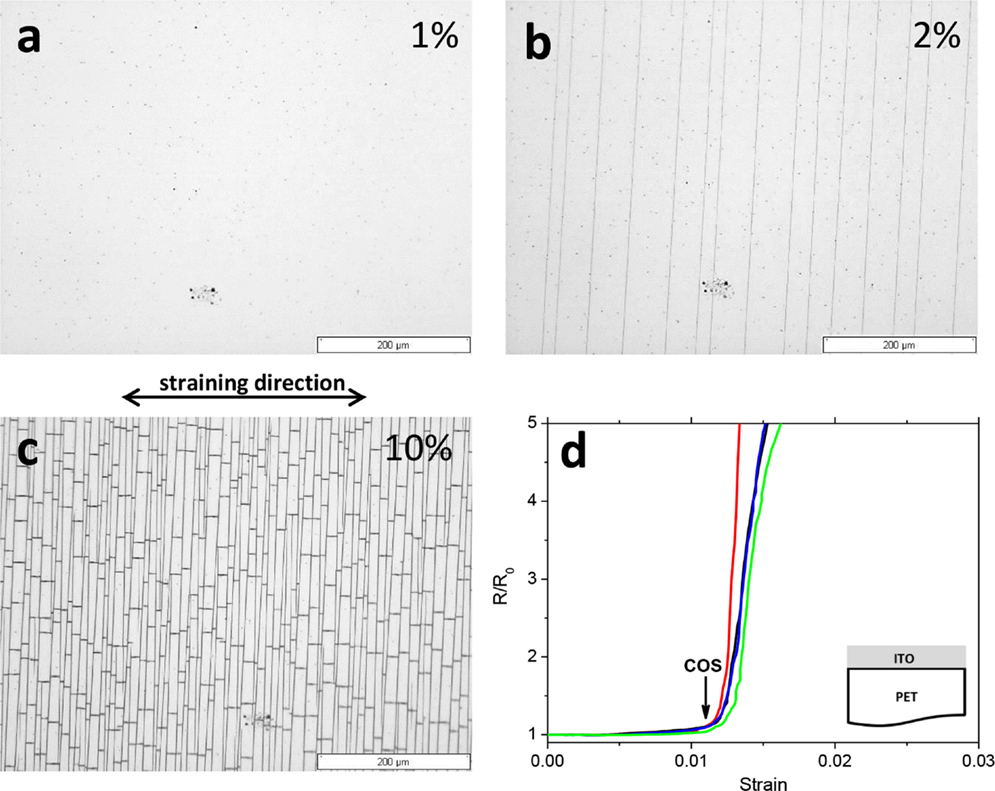
Figure 1. Tensile testing of a 100-nm thick ITO films on PET. (A–C) Optical images of the same surface area taken in situ at different applied strain values. (D) Electrical resistance of three ITO samples measured in situ during straining.
Using OLM or SEM, in situ methods provide information about the COS, crack spacing evolution, and even the buckling strain of brittle films. Other techniques have also been utilized to examine ductile and brittle film behavior. For example, in situ atomic force microscopy (AFM), X-ray diffraction (XRD), or confocal laser scanning microscopy (CLSM) provide further insight into the deformation mechanisms and buckling phenomena, which occur during straining. In situ AFM studies have been used to better compare ductile deformation with brittle fracture with the use of the deformation spacing and through thickness crack spacing (Cordill and Marx, 2013a,b) as well as buckle growth (Jin et al., 2011; Marx et al., 2015a). XRD studies have been fruitful in the investigation of microstructure effects, thickness, and even the role of interlayers (Olliges et al., 2008; Gruber et al., 2009; Marx et al., 2015b). The use of in situ CLSM imaging is a relatively new in situ method and delivers information in three dimensions similar to AFM without height or scanning area restrictions. This in situ imaging method is useful when studying interface adhesion with tensile-induced delaminations.
As it has been discussed, in situ fragmentation testing is valuable method for conductive thin films. However, the use of only one in situ observation method gives limited information on the electrical or mechanical behavior. More knowledge is learned about the combined electro-mechanical behavior through the use of multiple in situ techniques, such as AFM and 4PP, and has brought new insight about how the mechanical damage affects the electrical response of ductile films (Cordill et al., 2014a). New combinations of in situ fragmentation methods and the valuable information that can be obtained for conductive films will be the focus of this study. First, the combination of in situ XRD and 4PP provide precise fracture and buckling stresses as well as the crucial data about how stresses develop in multilayers. CLSM and 4PP can also be combined to study the connection between crack propagation and electrical behavior as well as for the study of interface adhesion.
Materials and Methods
To demonstrate the difference between ductile and brittle electro-mechanical behavior, Au and Cr films on polyimide are utilized. First, a 300-nm sputter deposited Au film on 50 μm thick PI was compared to the same 300-nm Au film with a 200-nm sputtered Cr overlayer. The Cr overlayer is used to aid in the delamination of the Au–PI interface when strained (Cordill et al., 2014b). The Au films were deposited using the working gas (Ar) pressure of 7.5 × 10⁻³ Torr at a power of 75 W DC as described by Yeager and Bahr (2010), and the Cr overlayer was deposited with an Ar working gas pressure of 1.5 × 10⁻³ Torr at 250 W DC power. A third film system consisting of a 50-nm Au film with a 10-nm Cr adhesion layer on PI was also deposited using the similar sputtering parameters but using 100-W DC power. This film system has been studied with other ex situ and in situ techniques and more information can be found in Putz et al. (2015, 2016). To demonstrate different adhesion theories, the 300-nm Au film with the 200-nm Cr overlayer was utilized as well as to two other gold systems. The first has a 10-nm Ta adhesion layer between the Au and PI while the second system has a 10-nm Ti adhesion layer between the Au and PI with an additional 200-nm Cr overlayer. The adhesion layers were sputter deposited before the 300-nm Au film without breaking vacuum (Yeager et al., 2008). The Cr overlayer was deposited after breaking vacuum in a different sputtering chamber using the parameters for Cr stated above. The film thicknesses were measured with focused ion beam cross-sections (not shown) after deposition.
Rectangular samples used for tensile straining were cut with a scalpel to the dimensions of approximately 7 mm × 35 mm. For in situ XRD experiments, samples were strained continuously to a maximum strain of 15% with a rate of 0.1 mm/min and then unloaded to a force F = 0 N with the same rate using an Anton Paar TS600 straining stage with 4PP resistance measurement incorporated into the grips. At the maximum strain, a hold period of 5 min was applied. The in situ synchrotron radiation measurements were carried out on the KMC-2 beamline (Erko et al., 2000) at BESSY II, Helmholtz-Zentrum Berlin für Materialien und Energie (HZB). The resistance probes were incorporated into the grips of the Anton Paar straining stage in a similar manner as described in Glushko and Cordill (2014b). These experiments were employed to measure the lattice strains, which develop in the Au films during continuous tensile straining. The tensile device was positioned so that the sample surface was in the reflection geometry to the incoming synchrotron X-ray beam. In situ XRD measurements were continuously performed with a beam size of 300 μm in diameter and a beam wavelength of 0.177 nm. The (111) reflections of the Au layer were recorded simultaneously with a Brucker VÅNTEC detector and an exposure time of 5 s at five different Ψ angles. Lattice strains were measured with the sin2 Ψ method (Spieß et al., 2005) [sin2 Ψ range 0–0.6 (−)]. A Pearson fit was applied to determine peak positions and peak widths. Film stresses were calculated using X-ray elastic constants (XECs) (1/2 S2) (Noyan and Cohen, 2013) for untextured (111) Au reflections. XECs were calculated from single-crystal elastic constants assuming the Hill model with the software ElastiX (Wern et al., 2002). Prior to and after the tensile experiment, residual lattice strains were measured with high resolution using 11 different Ψ angles. The lattice strain in the Cr overlayer was not analyzed because the Cr (110) peak overlaps with the Au (200) peak (see Figure S1 in Supplementary Material) and the response could not be separated, therefore, only the lattice strains which developed in the Au layers will be discussed. It was only possible to perform one experiment for the Au and Au with Cr overlayer samples due to the fact that they were performed at a synchrotron source. However, several experiments on similar samples have been performed and compare well to those presented.
More recently, CLSM has been utilized for in situ fragmentation testing of flexible electronic materials. CLSM is a 3D imaging technique that uses a scanned laser and precise stage movements to generate 3D images. It is similar to AFM, but imaging times are significantly shorter and larger areas can be accessed. Other advantages of CLSM are that there is no limitation in the z-direction (height) as with AFM, and the technique is ideal for transparent coatings. As an example, a 100-nm ITO film on PET that was mechanically bent under compression to form cracks and buckles is shown in Figure 2. With CLSM, the cracks as well as the buckles that formed at the crack fronts can be assessed (Figure 2B). In situ CSLM and 4PP experiments were also made using the same sample dimension and the Anton Paar TS 600 straining stage with the resistance measurements incorporated into the grips. CLSM imaging was performed with an Olympus LEXT OLS4100 during straining at a rate of 0.6 mm/min. The straining was stepwise so that an image could be obtained at each straining step during a 2-min hold period. From the obtained images, the crack spacing, λ, as a function of strain was measured using the software Image J (Abràmoff et al., 2004). All experiments were repeated at least once and the presented results illustrate representative behavior.
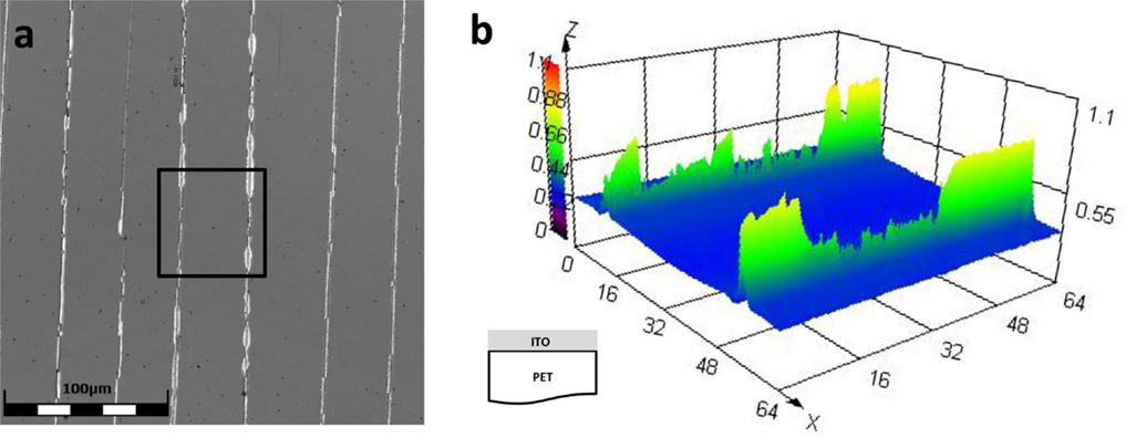
Figure 2. (A) CLSM laser image of 100-nm ITO film on PET after mechanical testing. (B) Color 3D height image of the box in (A) demonstrating the capabilities of CLSM with transparent conductors. The units in (B) are in microns (color online).
Results and Discussion
Combined X-Ray Diffraction and Electrical Resistance Fragmentation Testing
As it has been shown by many research groups (Gruber et al., 2008; Frank et al., 2009; Marx et al., 2015b), in situ XRD tensile straining can provide useful information on how thin film or coating thickness, microstructure, and deposition methods influence mechanical stresses and strains of flexible electronic materials. From the evolution of the lattice strains during straining, clear ductile or brittle material behavior is determined. With in situ 4PP, ductile and brittle films also have distinct electrical responses. When ductile films, such as Cu or Au, are strained, the response follows the theory (Eq. 2) and the film is said to have good “stretchability.” On the other hand, brittle films, like ITO (Figure 1D) deviate from theory, and the resistance dramatically increases. The combination of XRD and 4PP allows for the direct correlation between the COS and fracture stress, σf.
Figure 3A shows the ductile mechanical behavior of the 300-nm Au film on PI. The lattice strains increase to a maximum and then level off. The maximum lattice strain is equivalent to the stress of 400 MPa. Upon unloading, the lattice strains decrease into the compressive regime (−400 MPa). This is due to the fact that the film plastically deformed during straining (Figure 3B) and is now slightly longer than the PI substrate, which leads to the compressive behavior. The error bars arise from the linear fit of peak shift. The electrical response also illustrates ideal ductile behavior as the R/R0 follows the theoretical curve up to the maximum applied strain. When the load is removed, the R/R0 falls below the theoretical curve. The final R/R0 is about 8% higher than the original R/R0. The exact cause of the lower electrical response during unloading is still under investigation but could be due to the formation of localized thinned areas (necks) or grain growth as observed by some groups (Glushko and Cordill, 2014a; Cordill et al., 2016). Poststraining SEM (Figure 3B) only indicates some localized thinning and possible short through thickness cracks. With the current setup, it was not possible to strain higher than 15%. It would be beneficial to strain to 30–40% strain and to determine the COS of the Au film and the corresponding film lattice strains and stresses. However, the 300-nm Au film could be considered as a highly stretchable material and very suitable for flexible electronics because of its ideal electro-mechanical behavior.
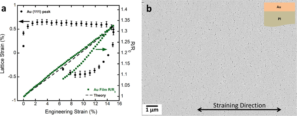
Figure 3. (A) In situ XRD and 4PP results of the 300-nm Au film on PI illustrating ductile film electro-mechanical behavior. Black circles are the lattice strains and green squares the electrical resistance. (B) SEM micrograph of the Au film surface after straining to 15% showing areas of localized thinning and possible through thickness cracks.
In contrast, the Au film with the Cr overlayer behaves in a brittle manner. As shown in Figure 4A of the in situ XRD and 4PP results, the lattice strains increase to a maximum, peak lattice strain and then rapidly decreases to a lower plateau at 6% strain. The peak lattice strain is approximately when the R/R0 deviates from theory. The sample broke at about 11% applied strain and the unloading of the sample was not recorded. From the combined experiment, the fracture stress, σf, of the Au film can be calculated from the peak lattice strain and is 540 MPa, slightly higher than the single Au film. The plateau of the lattice strains is related to the crack spacing saturation and delamination as known from other studies (Marx et al., 2015b). Once cracks form in the multilayer, the lattice strain (or stress) in the film is relieved, which causes the decrease. From Figure 4B, it can be observed that the Cr overlayer cracks which in turn causes cracks to form in the normally ductile Au film. The overlayer also aids the formation of buckles which can be utilized to evaluate the adhesion of the Au–PI interface and will be discussed in Section “Adhesion Measurements of Films on Polymer Substrates.”
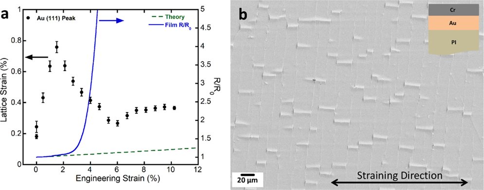
Figure 4. (A) In situ XRD and 4PP results of the 300-nm Au film with a 200-nm Cr overlayer on PI illustrating brittle film electro-mechanical behavior. (B) SEM micrograph after straining to 11% illustrating that cracks formed through both the Cr and Au films along with buckles.
What can be drawn from in situ XRD and 4PP experiments is a more precise measurement of the fracture stress necessary to determine the τIFSS as well as the correlation between the stress–strain response of individual films and the electrical response. These experiments also provide vital information about the behavior of multilayers as well as the fracture and deformation response. It has been demonstrated that the combination of ductile and brittle metal layers leads to very brittle electro-mechanical behavior. This is an important concept for flexible electronic devices. The influence of brittle overlayers and adhesion layers has been studied for metal films with in situ XRD (Cordill et al., 2014b; Marx et al., 2015b; Putz et al., 2015). However, further examination of how the brittle transparent conductors and encapsulation layers affect the metal conductors is necessary to determine how these brittle layers influence the electro-mechanical behavior of a flexible electronic device. It should be noted that in situ XRD studies can only be utilized for crystalline materials. As many transparent conductors are amorphous, stress analyzes with X-rays are not possible. However, Raman spectroscopy has been successfully employed to study stresses in diamond-like carbon (DLC) films and is an alternative to XRD for transparent coatings (Ahmed et al., 2011).
In situ Fragmentation Testing with Confocal Laser Scanning Microscopy
As an example of in situ CSLM and 4PP fragmentation testing, a 50-nm Au film with a 10-nm Cr adhesion layer on PI is shown in Figure 5. Here, the combination of CSLM and 4PP allows for the further examination of how cracks influence the electrical behavior. As shown in Figure 5, the film does not crack until about 2% strain. After this point, the R/R0 deviates from theory and continues to increase until the maximum applied strain of 14%. The crack spacing decreases until reaching a plateau at approximately 7–8% when no further cracks form. Interestingly, when the load is removed, the R/R0 is reduced to 4 from the maximum R/R0 of 32 (red triangle in Figure 5D). That indicates the closing of cracks allowing current to flow again. It is clearly observed that the normally ductile Au film cracks like a brittle film due to the presence of the Cr adhesion layer. This is a further example of how the use of brittle layers detrimentally affects the stretchability of ductile materials. Additionally, in Figure 5A, the first appearance of cracks is along a diagonal to the straining direction. These cracks are a consequence of scratches in the substrate and illustrate that proper preparation of the substrate is also a crucial factor affecting the COS and stretchability of flexible electronic devices. Finally, with the combination of CLSM (or OLM) and 4PP a better understanding of how the crack density and electrical response are related. For example, when the R/R0 deviates from theory, many cracks are present in the film (Figure 5A), and it is not one crack that causes the resistance to increase. It is also of interest as to why the R/R0 continues to increase even after the crack saturation is reached. An improved understanding of the crack density and R/R0 would be beneficial for metal thin films and transparent conductors.
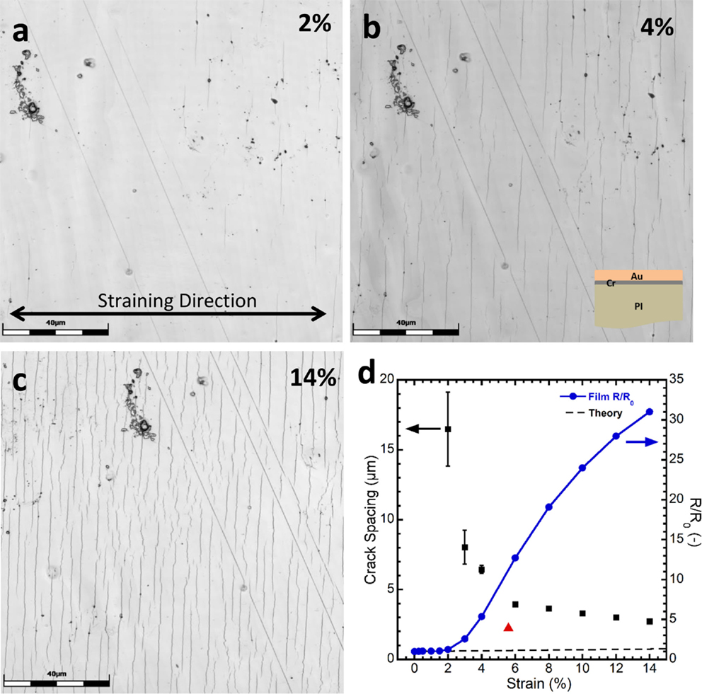
Figure 5. Example of an in situ fragmentation test with CLSM and 4PP on a 50-nm Au film with a 10-nm Cr adhesion layer. (A) At 2% strain, cracks have initiated and caused an increase in the resistance. (B) Same area of film after 4% strain, (C) after 14% strain and crack saturation. (D) Corresponding crack spacing (black squares) and R/R0 response (blue circles, connecting line has no mathematical meaning) illustrating the correlation between crack spacing and COS as well as resistance recovery upon unloading (red triangle). Scale bars in (A–C) are 40 μm (color online).
Confocal laser scanning microscopy also allows for the examination of the crack fragment shape and buckle formation during straining. As an example, the same 300-nm Au film with the 200-nm Cr overlayer from Figure 4 was also strained in situ with CLSM and three straining steps are shown in Figures 6A–C. Because CLSM obtains 3D surface images, further information about how stress is transferred across the film fragments and buckle propagation is obtained. In order to apply the shear lag theory to determine the τIFSS, the theory assumes that the interface between the film and substrate remains coplanar. This occurs for ceramic films on metal substrates (Agrawal and Raj, 1989) but is not always true for metal and ceramic films on polymer substrates. Instead, the film fragments bend or curve between the through thickness crack (Figure 6D) and has thus far only been observed with in situ AFM fragmentation (Douville et al., 2011; Taylor et al., 2012) and finite element modeling (Toth et al., 2013). This phenomena have not been experimentally studied much due to the complicated and time consuming in situ AFM testing method. This out of plane deflection can lead to a deviation of the mechanical predictions due to the assumptions in the shear lag theory. When the interface is coplanar to the loading axis, the load can be transferred to the film through shear at the interface. However, loading at the interface causes the film fragment to curve and the amount of curvature depends on the elastic modulus of the film and substrate. Polymer substrates generally have small elastic moduli compared to metal substrates and this is why the film fragment curvature is visible. The curving of the film fragments complicates the mechanics of the whole system and greatly influences the resulting crack density due to the fact that now not only shear stresses but also bending stresses are present (Taylor et al., 2012). With CLSM, the nature and curvature of the film fragments can be better studied as a function of applied strain, crack density, and film thickness.
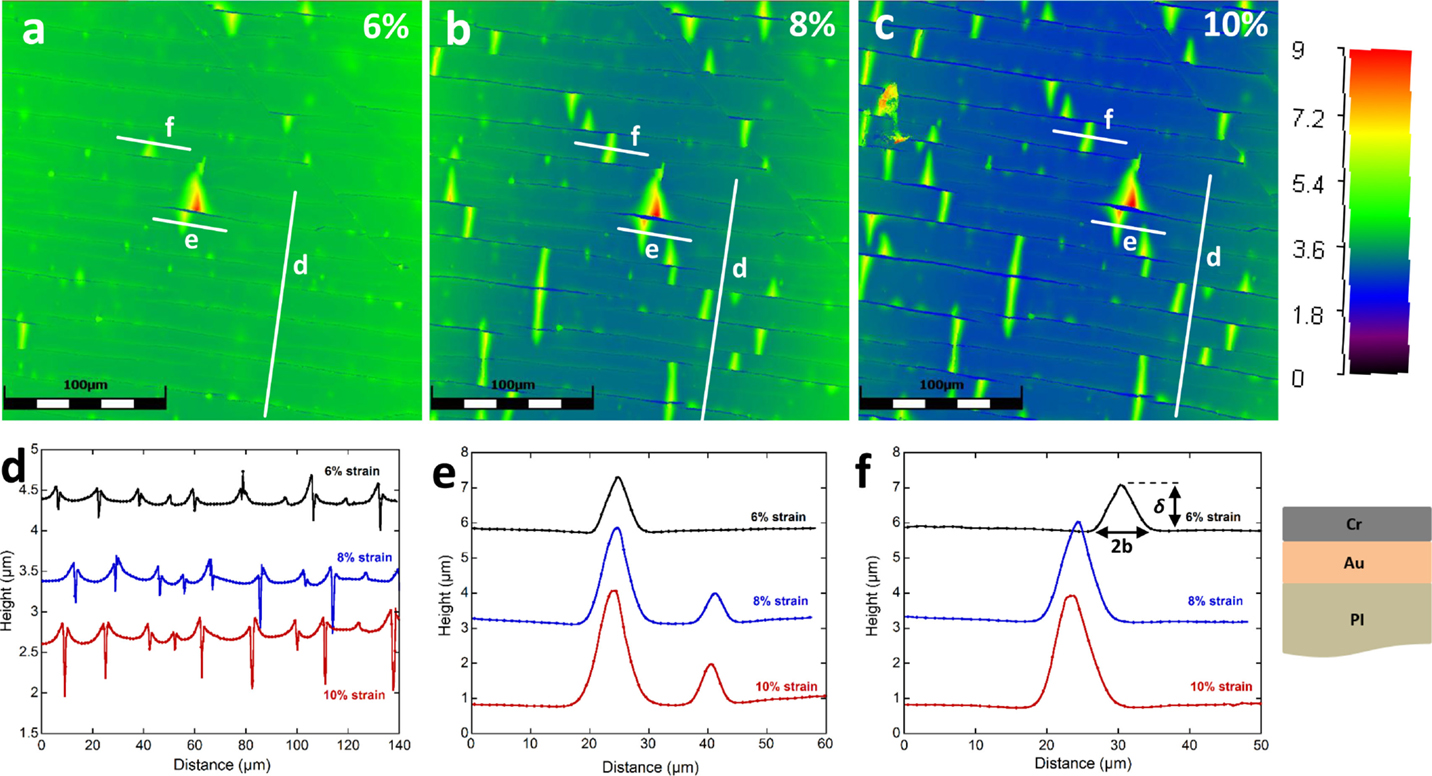
Figure 6. CLSM color height images (color scale at right in μm) of the 300-nm Au film with 200-nm Cr overlayer at (A) 6% strain, (B) 8% strain, and (C) 10% strain [scale bar in (A)–(C) is 100 μm]. (D) Height profiles perpendicular to the cracks illustrating that the film fragments curve between the cracks. Buckle growth can also be studied with CLSM as shown in (E,F) (color online).
Buckle delamination can also be examined in depth with in situ CLSM. Using the height information, the buckle growth can be observed as a function of strain. Examples of buckle growth are shown in Figures 6E,F. The buckles increase their height and width with increasing strain, and in Figure 6E, the growth and propagation of a second buckle can be analyzed. The addition of height information also identifies where buckles may be more susceptible to initiate and may also shed light on why buckles tend to form in clusters. With this new experimental approach, researchers will be able to address these issues and provide predictive models to better understand delamination failure.
Adhesion Measurements of Films on Polymer Substrates
There are two main models used to quantitatively measure the interfacial adhesion of thin films on polymer substrates. The well-known Hutchinson and Suo (1992) model has been mostly applied to buckles, which form spontaneously on rigid substrates and the tensile-induced delamination model, which was developed especially for hard films on compliant polymer substrates (Cordill et al., 2010). The Hutchinson and Suo model utilizes buckle delaminations that form spontaneously or due to an applied compressive stress (Coupeau et al., 1999; Cleymand et al., 2000; Parry et al., 2005). As has been previously shown, compressive stresses can arise in a film during unloading of a tensile strain for some film-substrate systems (see Figure 3A). For example, a 300-nm Au film with a 10-nm Ta adhesion layer on PI was strained to incrementally larger maximum engineering strains and unloaded to a load of 0 N with in situ CLSM (Figure 7). At the maximum applied strains and unloaded strains, images were made of the film surface. After applying 4% strain and unloading to 0 N, buckles formed perpendicular to the straining direction, as shown in Figure 7B. With increased strains, the buckles continued to propagate across the width of the sample. With the height images, the half buckle width, b, and the buckle height, δ, can be measured and used to calculate the mixed mode adhesion energy of the Ta–PI interface,
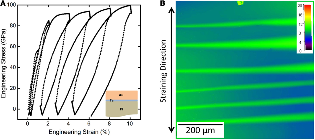
Figure 7. (A) Tensile loading curve of a 300-nm Au film with a 10-nm Ta adhesion layer on PI. (B) When the load was removed (decreased to 0 N) buckles form perpendicular to the straining direction and can be used to calculate the adhesion energy of the interface.
In Eq. 3, h is the film thickness, E is the elastic modulus of the film, υ is the Poisson’s ratio of the film, σd is the driving stress, σb is the buckling stress, and Ψ is the phase angle of loading. Formulations for the driving and buckling stresses can be found in references (Hutchinson and Suo, 1992; Cordill et al., 2004). Using the Hutchinson and Suo model, the adhesion energy was calculated to be Γ(Ψ) = 9.8 ± 2.8 Jm−2. The adhesion measurement would not have been possible without CLSM because the buckle heights are between 4 and 7 μm, greater than what a commercial AFM could measure. In addition, the areas that can be observed are also much larger compared to what can easily be imaged with the AFM and provide more buckle measurements for valuable statistics.
The second model used to measure the adhesion of films on polymer substrates is tensile-induced delamination. This method is based on fragmentation testing and can produce well-defined areas of delamination between the crack fragments as shown in Figures 4B, 6A–C, and 8A. Once the crack spacing has reached the saturation regime, the films can delaminate between the crack fragments in the form of buckles (Figure 8A). These induced buckles can be utilized to measure the adhesion energy of the interface (Cordill et al., 2010). In the example shown in Figure 8A, a 200-nm Cr overlayer on a 300-nm Au film with a 10-nm Ti adhesion layer on PI was strained and imaged with CLSM. Again, using the height images of the surface, the buckle dimensions (b and δ) can be measured and plotted as the as a function of (b/h), where h is the total film thickness (Figure 8B). The data is fit using Eq. 4 and a minimum α value to the minimum data,
and
where modified elastic modulus is and Γ is the adhesion energy (Cordill et al., 2010). In this case, the modified elastic modulus was thickness weighted to take into account the Cr and Au properties (Cordill et al., 2014b). For this film system and buckles, an α = 0.000015 was used to calculate an adhesion energy of Γ = 1.9 ± 0.7 Jm−2 (Figure 8B). The standard deviation is from small changes in α (±0.000005). Further information on the model can be found in Cordill et al. (2010, 2014b). As a comparison, the Hutchinson and Suo model (Hutchinson and Suo, 1992) was also employed due to the fact that the buckles had an ideal shape similar to spontaneously delaminated buckles. Using the same buckle measurements and Eq. 3, an adhesion energy of Γ(Ψ) = 1.1 ± 0.5 was calculated. The two models achieve similar adhesion values indicating that either model could be employed for these buckles. With the quantitative measurement of the adhesion, it can be concluded that a Ta adhesion layer is better at improving the adhesion of Au to PI than a Ti adhesion layer. The Ta adhesion layer increased the interfacial energy by almost a factor of 10 compared to the Ti adhesion layer. These results follow that of Yeager et al. (2008) who used four point bending to measure the adhesion of TiW–PI and Ta–PI interface.
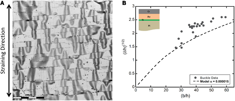
Figure 8. (A) CLSM laser image of the delaminated Cr/Au/Ti film from PI. (B) Using the tensile-induced delamination model and a minimum α-values of 0.00015, the adhesion energy was determined to be Γ = 1.9 ± 0.7 Jm−2.
In order to apply these adhesion models, especially tensile-induced delamination, it is best to use the first buckles that form (Cordill et al., 2010). The initial buckles have a more rounded shape as required by the model and are not cracked at the buckle apex. With further straining, the buckles tend to become more pointed and tent-like because a crack forms at the buckle apex to relieve stress. An example can be viewed in Figure 6. As the strain is increased, the buckles in Figures 6E,F become more pointed. To measure the adhesion energy of this film system, only buckles in Figure 6A were used. Because CLSM was employed for this in situ experiment, straining did not have stopped once the buckles formed. Rather, the experiment was continued to study both adhesion and buckle formation with the same experiment. The adhesion energy of the Cr–Au–PI film system of Figure 6 was measured to be Γ = 19 ± 7 Jm−2, indicating that adhesion layers are not necessary for this system because the systems with adhesion layers had lower measured adhesion energies (9.8 and 1.7 Jm−2, respectively, for Ta and Ti). These same methods and models can be applied to transparent conductive films to assess the adhesion energies.
Conclusion
As flexible electronics become part of everyday life, it is necessary to understand better how the different materials interact and fail. Combined in situ electro-mechanical fragmentation testing is a useful technique to assess both the electrical and mechanical failure mechanisms. Fragmentation testing has moved from simple optical observations of the COS to more advanced studies using X-rays and CSLM. It can been demonstrated that in situ XRD and 4PP experiments provide useful data on single-layer ductile film deformation and multi-layer brittle fracture. The electro-mechanical results on multilayers should be further considered due to the fact that flexible devices are composed of many layers, from the brittle transparent conductors and encapsulation layers to the ductile metal interconnects. The consequence of multilayers is a more brittle behaving system both electrically and mechanically. An improved understanding of how all of the layers fail electrically and mechanically is needed in order to better design robust devices and thus more research in this direction. CLSM is an imaging method that is new to in situ fragmentation studies. The power of CLSM is the 3D imaging of virtually any surface, transparent or reflective. The use of in situ CLSM and 4PP can be employed to better understand the correlation between crack propagation and electrical resistance. The adhesion of interfaces can also be measured with CLSM because larger areas and larger heights (z-range) are assessable with this method. Through the use of these advanced characterization methods, more insight and an improved understanding of correlated electrical and mechanical failure can be achieved, leading to more robust flexible electronics.
Author Contributions
MC is the main author of the text and performed several of the experiments presented. The adhesion analysis was also performed by MC. OG wrote sections of the introduction and is responsible for the in situ 4PP setup and measurements that are presented. BP was responsible for the XRD analysis and the AuCr experiments.
Conflict of Interest Statement
The authors declare that the research was conducted in the absence of any commercial or financial relationships that could be construed as a potential conflict of interest.
Funding
This work was partially supported by the Austrian Science Fund (FWF) through project P22648-N20. The Helmholtz Zentrum für Materialien und Energie (Berlin, Germany) under the proposal number 15101992-ST and the assistance of D. Többens at the synchrotron source BESSY II is gratefully acknowledged. The confocal laser scanning microscopy images were made possible through a 2014 Olympus Technology Grant.
Supplementary Material
The Supplementary Material for this article can be found online at http://journal.frontiersin.org/article/10.3389/fmats.2016.00011
References
Abràmoff, M. D., Magalhães, P. J., and Ram, S. J. (2004). Image processing with imageJ. Biophotonics Int. 11, 36–41.
Agrawal, D. C., and Raj, R. (1989). Measurement of the ultimate shear strength of a metal-ceramic interface. Acta Metall. 37, 1265–1270. doi: 10.1016/0001-6160(89)90120-X
Ahmed, F., Bayerlein, K., Rosiwal, S. M., Göken, M., and Durst, K. (2011). Stress evolution and cracking of crystalline diamond thin films on ductile titanium substrate: analysis by micro-Raman spectroscopy and analytical modelling. Acta Mater. 59, 5422–5433. doi:10.1016/j.actamat.2011.05.015
Ahn, S. H., and Guo, L. J. (2008). High-speed roll-to-roll nanoimprint lithography on flexible plastic substrates. Adv. Mater. 20, 2044–2049. doi:10.1002/adma.200702650
Andersons, J., Tarasovs, S., and Leterrier, Y. (2009). Evaluation of thin film adhesion to a compliant substrate by the analysis of progressive buckling in the fragmentation test. Thin Solid Films 517, 2007–2011. doi:10.1016/j.tsf.2008.10.072
Cleymand, F., Coupeau, C., Colin, J., and Grilhe, J. (2000). Interactive study of straight-sided buckling patterns in thin films under compressive stress. Eur. Phys. J. Appl. Phys. 10, 3–7. doi:10.1051/epjap:2000113
Cordill, M. J., Bahr, D. F., Moody, N. R., and Gerberich, W. W. (2004). Recent developments in thin film adhesion measurement. IEEE Trans. Device Mater. Reliab. 4, 163–168. doi:10.1109/TDMR.2004.829071
Cordill, M. J., Berger, J., Glushko, O., Marx, V. M., and Kirchlechner, C. (2016). Effect of microstructure on the electro-mechanical behavior of Cu films on polyimide. JOM (in press).
Cordill, M. J., Fischer, F. D., Rammerstorfer, F. G., and Dehm, G. (2010). Adhesion energies of Cr thin films on polyimide determined from buckling: experiment and model. Acta Mater. 58, 5520–5531. doi:10.1016/j.actamat.2010.06.032
Cordill, M. J., Glushko, O., Kreith, J., Marx, V. M., and Kirchlechner, C. (2014a). Measuring electro-mechanical properties of thin films on polymer substrates. Microelectron. Eng. 137, 96–100. doi:10.1016/j.mee.2014.08.002
Cordill, M. J., Marx, V. M., and Kirchlechner, C. (2014b). Ductile film delamination from compliant substrates using hard overlayers. Thin Solid Films 571, 302–307. doi:10.1016/j.tsf.2014.02.093
Cordill, M. J., and Marx, V. M. (2013a). Fragmentation testing for ductile thin films on polymer substrates. Philos. Mag. Lett. 93, 618–624. doi:10.1080/09500839.2013.830792
Cordill, M. J., and Marx, V. M. (2013b). In-situ tensile straining of metal films on polymer substrates under and AFM. MRS Proc. 1527, 2–7. doi:10.1557/opl.2013.617
Cordill, M. J., Taylor, A. A., Berger, J., Schmidegg, K., and Dehm, G. (2012). Robust mechanical performance of chromium-coated polyethylene terephthalate over a broad range of conditions. Philos. Mag. 92, 3346–3362. doi:10.1080/14786435.2012.700418
Cordill, M. J., Taylor, A. A., and Schmidegg, K. (2011). Thickness effects on the fracture of chromium films on polyethylene terephthalate. BHM Berg- und Hüttenmännische Monatshefte 156, 434–437. doi:10.1007/s00501-011-0032-1
Coupeau, C., Naud, J. F., Cleymand, F., Goudeau, P., and Grilhé, J. (1999). Atomic force microscopy of in situ deformed nickel thin films. Thin Solid Films 353, 194–200. doi:10.1016/S0040-6090(99)00369-7
Cox, H. L. (1952). The elasticity and strength of paper and other fibrous materials. Br. J. Appl. Phys. 3, 72–79. doi:10.1088/0508-3443/3/3/302
Douville, N. J., Li, Z., Takayama, S., and Thouless, M. D. (2011). Fracture of metal coated elastomers. Soft Matter 7, 6493–6500. doi:10.1039/c1sm05140g
Dupont, S. R., Oliver, M., Krebs, F. C., and Dauskardt, R. H. (2012). Interlayer adhesion in roll-to-roll processed flexible inverted polymer solar cells. Sol. Energy Mater. Sol. Cells 97, 171–175. doi:10.1016/j.solmat.2011.10.012
Erko, A., Packe, I., Hellwig, C., Fieber-Erdmann, M., Pawlizki, O., Veldkamp, M., et al. (2000). “KMC-2: the new X-ray beamline at BESSY II,” in Synchrotron Radiation Instrumentation: SRI99: Eleventh US National Conference, eds P. Pianetta, J. Arthur, and S. Brennan (Stanford, CA: AIP Publishing), 415–418.
Forrest, S. R. (2004). The path to ubiquitous and low-cost organic electronic appliances on plastic. Nature 428, 911–918. doi:10.1038/nature02498
Frank, S., Handge, U. A., Olliges, S., and Spolenak, R. (2009). The relationship between thin film fragmentation and buckle formation: synchrotron-based in situ studies and two-dimensional stress analysis. Acta Mater. 57, 1442–1453. doi:10.1016/j.actamat.2008.11.023
Gamerith, S., Klug, A., Scheiber, H., Scherf, U., Moderegger, E., and List, E. J. W. (2007). Direct ink-jet printing of Ag-Cu nanoparticle and Ag-precursor based electrodes for OFET applications. Adv. Funct. Mater. 17, 3111–3118. doi:10.1002/adfm.200600762
Glushko, O., and Cordill, M. J. (2014a). Electrical resistance decrease due to grain coarsening under cyclic deformation. JOM 66, 1–4. doi:10.1007/s11837-014-0943-x
Glushko, O., and Cordill, M. J. (2014b). Electrical resistance of metal films on polymer substrates. Exp. Tech. 1–8. doi:10.1111/ext.12082
Glushko, O., Marx, V. M., Kirchlechner, C., Zizak, I., and Cordill, M. J. (2014). Recovery of electrical resistance in copper films on polyethylene terephthalate subjected to a tensile strain. Thin Solid Films 552, 141–145. doi:10.1016/j.tsf.2013.12.055
Gruber, P. A., Arzt, E., and Spolenak, R. (2009). Brittle-to-ductile transition in ultrathin Ta/Cu film systems. J. Mater. Res. 24, 1906–1918. doi:10.1557/jmr.2009.0252
Gruber, P. A., Böhm, J., Onuseit, F., Wanner, A., Spolenak, R., and Arzt, E. (2008). Size effects on yield strength and strain hardening for ultra-thin Cu films with and without passivation: a study by synchrotron and bulge test techniques. Acta Mater. 56, 2318–2335. doi:10.1016/j.actamat.2008.01.027
Huang, H., and Spaepen, F. (2000). Tensile testing of free-standing Cu, Ag and Al thin films and Ag/Cu multilayers. Acta Mater. 48, 3261–3269. doi:10.1016/S1359-6454(00)00128-2
Hutchinson, J. W., and Suo, Z. (1992). Mixed mode cracking in layered materials. Adv. Appl. Mech. 29, 63–191. doi:10.1016/S0065-2156(08)70164-9
Jin, H., Lu, W. Y., Cordill, M. J., and Schmidegg, K. (2011). In situ study of cracking and buckling of chromium films on PET substrates. Exp. Mech. 51, 219–227. doi:10.1007/s11340-010-9359-x
Kelly, A., and Tyson, W. R. (1965). Tensile properties of fibre-reinforced metals: copper/tungsten and copper/molybdenum. J. Mech. Phys. Solids 13, 329–350. doi:10.1016/0022-5096(65)90035-9
Leterrier, Y., Boogh, L., Andersons, J., and Manson, J.-A. E. (1997). Adhesion of silicon oxide layers on poly(ethylene terephthalate). I: effect of substrate properties on coating’s fragmentation process. J. Polym. Sci. Part B Polym. Phys. 35, 1449–1461. doi:10.1002/(SICI)1099-0488(19970715)35:9<1449::AID-POLB15>3.0.CO;2-6
Lohmiller, J., Woo, N. C., and Spolenak, R. (2010). Microstructure-property relationship in highly ductile Au-Cu thin films for flexible electronics. Mater. Sci. Eng. A 527, 7731–7740. doi:10.1016/j.msea.2010.08.043
Lu, N., Wang, X., Suo, Z., and Vlassak, J. (2009). Failure by simultaneous grain growth, strain localization, and interface debonding in metal films on polymer substrates. J. Mater. Res. 24, 379–385. doi:10.1557/JMR.2009.0048
Lu, N., Wang, X., Suo, Z., and Vlassak, J. J. (2007). Metal films on polymer substrates stretched beyond 50%. Appl. Phys. Lett. 91, 221909. doi:10.1063/1.2817234
Marx, V. M., Kirchlechner, C., Zizak, I., Cordill, M. J., and Dehm, G. (2015a). Adhesion measurement of a buried Cr interlayer on polyimide. Philos. Mag. 95, 1982–1991. doi:10.1080/14786435.2014.920543
Marx, V. M., Toth, F., Wiesinger, A., Berger, J., Kirchlechner, C., Cordill, M. J., et al. (2015b). The influence of a brittle Cr interlayer on the deformation behavior of thin Cu films on flexible substrates: experiment and model. Acta Mater. 89, 278–289. doi:10.1016/j.actamat.2015.01.047
Noyan, I. C., and Cohen, J. B. (2013). Residual Stress: Measurement by Diffraction and Interpretation. New York: Springer-Verlag.
Olliges, S., Gruber, P. A., Orso, S., Auzelyte, V., Ekinci, Y., Solak, H. H., et al. (2008). In situ observation of cracks in gold nano-interconnects on flexible substrates. Scr. Mater. 58, 175–178. doi:10.1016/j.scriptamat.2007.09.037
Parry, G., Colin, J., Coupeau, C., Foucher, F., Cimetiere, A., and Grilhe, J. (2005). Effect of substrate compliance on the global unilateral post-buckling of coatings: AFM observations and finite element calculations. Acta Mater. 53, 441–447. doi:10.1016/j.actamat.2004.09.039
Peng, C., Jia, Z., Bianculli, D., Li, T., and Lou, J. (2011). In situ electro-mechanical experiments and mechanics modeling of tensile cracking in indium tin oxide thin films on polyimide substrates. J. Appl. Phys. 109, 1–8. doi:10.1063/1.3592341
Putz, B., Glushko, O., Marx, V. M., Kirchlechner, C., Toebbens, D. M., and Cordill, M. J. (2016). Electro-mechanical performance of thin gold films on polyimide. MRS Proc. (in press).
Putz, B., Schoeppner, R. L., Glushko, O., Bahr, D. F., and Cordill, M. J. (2015). Improved electro-mechanical performance of gold films on polyimide without adhesion layers. Scr. Mater. 102, 23–26. doi:10.1016/j.scriptamat.2015.02.005
Spieß, L., Teichert, G., Schwarzer, R., Behnken, H., and Genzel, C. (2005). Moderne röntgenbeugung. Wiesbaden: Teubner.
Tarasovs, S., Andersons, J., and Leterrier, Y. (2010). Estimation of interfacial fracture toughness based on progressive edge delamination of a thin transparent coating on a polymer substrate. Acta Mater. 58, 2948–2956. doi:10.1016/j.actamat.2010.01.023
Taylor, A. A., Cordill, M. J., Bowles, L., Schalko, J., and Dehm, G. (2013). An elevated temperature study of a Ti adhesion layer on polyimide. Thin Solid Films 531, 354–361. doi:10.1016/j.tsf.2013.01.016
Taylor, A. A., Cordill, M. J., and Dehm, G. (2012). On the limits of the interfacial yield model for fragmentation testing of brittle films on polymer substrates. Philos. Mag. 92, 3363–3380. doi:10.1080/14786435.2012.723145
Taylor, A. A., Edlmayr, V., Cordill, M. J., and Dehm, G. (2011). The effect of film thickness variations in periodic cracking: analysis and experiments. Surf. Coatings Technol. 206, 1830–1836. doi:10.1016/j.surfcoat.2011.07.047
Toth, F., Rammerstorfer, F. G., Cordill, M. J., and Fischer, F. D. (2013). Detailed modelling of delamination buckling of thin films under global tension. Acta Mater. 61, 2425–2433. doi:10.1016/j.actamat.2013.01.014
Vellinga, W. P., De Hosson, J. T. M., and Bouten, P. C. P. (2011). Direct measurement of intrinsic critical strain and internal strain in barrier films. J. Appl. Phys. 110, 7. doi:10.1063/1.3624582
Wagner, S., and Bauer, S. (2012). Materials for stretchable electronics. MRS Bull. 37, 207–213. doi:10.1557/mrs.2012.37
Wern, H., Koch, N., and Maas, T. (2002). “Selfconsistent calculation of the x-ray elastic constants of polycrystalline materials for arbitrary crystal symmetry,” in Materials Science Forum, 127–132. Available at: http://www.scopus.com/inward/record.url?eid=2-s2.0-0036433960&partnerID=tZOtx3y1
Yeager, J. D., and Bahr, D. F. (2010). Microstructural characterization of thin gold films on a polyimide substrate. Thin Solid Films 518, 5896–5900. doi:10.1016/j.tsf.2010.05.070
Keywords: thin films, fragmentation, electrical resistance, cracking, X-ray diffraction
Citation: Cordill MJ, Glushko O and Putz B (2016) Electro-Mechanical Testing of Conductive Materials Used in Flexible Electronics. Front. Mater. 3:11. doi: 10.3389/fmats.2016.00011
Received: 30 December 2015; Accepted: 08 February 2016;
Published: 22 February 2016
Edited by:
Theodoros Dimopoulos, AIT – Austrian Institute of Technology, AustriaReviewed by:
Llibertat Abad Muñoz, Institut de Microelectrònica de Barcelona (IMB-CNM-CSIC), SpainLola González-García, INM – Leibniz Institute for New Materials, Germany
Copyright: © 2016 Cordill, Glushko and Putz. This is an open-access article distributed under the terms of the Creative Commons Attribution License (CC BY). The use, distribution or reproduction in other forums is permitted, provided the original author(s) or licensor are credited and that the original publication in this journal is cited, in accordance with accepted academic practice. No use, distribution or reproduction is permitted which does not comply with these terms.
*Correspondence: Megan J. Cordill, bWVnYW4uY29yZGlsbEBvZWF3LmFjLmF0