 H. Jessica Pereira
 Ross A. Hatton
- Department of Chemistry, University of Warwick, Coventry, United Kingdom
We report a copper–zinc oxide bilayer electrode supported on flexible polyethylene terephthalate (PET) with a sheet resistance of 11. 3 Ω sq−1 and average transparency of 84.6% in the wavelength range of 400–800 nm. The copper film is perforated with a dense array of sub-micron diameter apertures fabricated using polymer-blend lithography, which imparts broad band anti-reflectivity. We demonstrate proof-of-principle that it is possible to fabricate the polymer mask by dip coating which is a scalable deposition method compatible with roll-to-roll processing. During storage of the electrode at ambient temperature the ZnO layer is spontaneously doped with copper from the underlying copper film and so the thin ZnO layer serves both as an anti-reflecting layer and an excellent electron transport layer. When compared with commercially available indium tin oxide coated (ITO) plastic substrates this electrode exhibits superior stability towards bending deformation, with no change in sheet resistance after bending through a 4 mm radius of curvature 100 times. Model inverted organic photovoltaic (OPV) devices using this electrode exhibit a champion power conversion efficiency of ~8.7%, which is the highest reported efficiency to date for an OPV device using a copper based transparent electrode, outperforming identical devices using ITO coated plastic as the transparent electrode.
Introduction
The low cost associated with processing organic semiconductors by printing, together with the low processing temperature and color tuneability make organic photovoltaics (OPVs) attractive for a diverse range of applications (Kippelen et al., 2009; Ierides et al., 2019). The flexibility and light weight of OPVs supported on flexible plastic substrates also enables integration into wearable electronics, roofing, automobile and building related applications where conventional rigid photovoltaics are not suitable (Mohammad Bagher, 2014; Stoppa and Chiolerio, 2014; Zamarayeva et al., 2017; Meng et al., 2018; Cui et al., 2019), as well as enabling compact storage for transportation. All OPVs require a transparent electrode with low sheet resistance, which is often expressed in terms of the Haacke figure-of-merit (FoM), defined as the average transmittance (Tavg) raised to the power of 10 and divided by the electrode sheet resistance (Rsh) (Haacke, 1976, 1977; Garner, 2017). In addition to requiring a high Haacke FoM, flexible OPVs require a transparent electrode that does not degrade when bent, both for application purposes and for compatibility with roll-to-roll processing. Whilst ITO and fluorine doped tin oxide are predominantly used for research scale OPVs, due to their high Haacke FoM, they are unsuitable for flexible OPVs because of the inherent brittleness of the oxide films (Alzoubi et al., 2011; Galagan et al., 2011; Zou et al., 2014) which causes the Rsh to degrade readily upon modest physical deformation (De Arco et al., 2010; Alzoubi et al., 2011; Galagan et al., 2011; Rathmell and Wiley, 2011; Stec and Hatton, 2012; Zou et al., 2014). Consequently, flexible OPVs reported to date use a transparent electrode composed of carbon nanotubes (Yu et al., 2016), metal nanowires (Hu et al., 2011; Rathmell and Wiley, 2011; Lee et al., 2012), graphene (De Arco et al., 2010; Park et al., 2015), metal nanogrids (Galagan et al., 2011; Hu et al., 2011), or optically-thin (6–12 nm) films of gold (Au), silver (Ag) or copper (Cu) (Hu et al., 2011; Zou et al., 2014; Table S1). Of the metals, Ag is by far the dominant choice due to its relatively slow oxidation under ambient conditions, high electrical conductivity and its very low optical losses in the visible and infra-red regions (West et al., 2010; Naik et al., 2013). However, Ag is a costly metal and so Cu is attractive as an alternative because it offers a comparable conductivity at one hundredth of the cost (West et al., 2010; Pereira et al., 2017). Unfortunately, parasitic absorption in Cu due to inter-band absorption losses mean that optically-thin Cu films are not as transparent as Ag films of the same thickness (Burdick, 1963; West et al., 2010; Pereira et al., 2017, 2018). To address this we have recently reported a powerful bio-inspired method for increasing the far-field transparency of optically-thin Cu films on glass, based on incorporating a random distribution of ~100 million sub-micron diameter holes cm−2 which simultaneously reduces absorption losses whilst suppressing losses due to reflection (Pereira et al., 2018). Herein we advance that work by showing that: (i) the method of electrode fabrication can be translated to the a technologically important transparent plastic substrate polyethylene terephthalate (PET) with only slight adaptation, and that the Haacke FoM can be increased substantially above that previously-reported on glass substrates with a small increase the aperture density; (ii) it is possible to fabricate the polymer mask by dip coating, which, unlike spin coating, is a scalable deposition method compatible with roll-to-roll processing; (iii) these electrodes outperform ITO coated plastic as the transparent electrode in flexible OPVs.
Materials and Methods
Substrate Cleaning
Substrate slides of the required dimension (13 × 13 mm for OPV devices and 26 × 26 mm for electrode characterization) were cut from a roll of PET (Mitsubishi, Hostaphan GN 125 4600 A) and cleaned by rinsing consecutively in a diluted solution of surfactant, deionized water, acetone, and IPA for 30 min each followed by drying with a stream of nitrogen and UV/O3 treatment for 15 min. Notably both sides of the PET sheet were not identical in surface roughness and so Atomic Force Microscope (AFM) imaging was performed in tapping mode using an Asylum Research MFP−3D AFM to identify the smooth side onto which all surface treatment was done prior to deposition of Cu.
Mixed Monolayer Deposition
A mixed monolayer metal nucleation layer was deposited onto the PET substrates prior to evaporation of Cu, by exposing the substrates to vapors of 3-mercaptopropyltrimethoxysilane (MPTMS, Sigma Aldrich) and 3-aminopropyltrimethoxysilane (APTMS, Sigma Aldrich) at 50 mbar for 4 h immediately after UV/O3 treatment.
Deposition of Cu
Cu (11 nm) was deposited by thermal evaporation of Cu pellets at a rate of 2.2–2.5 Å s−1 to give the required thickness. All electrode and device fabrication was carried out in a nitrogen filled glove box with an O2 level <1 ppm unless otherwise stated. Evaporation of metals and metal oxides was carried out with a CreaPhys Organic Molecular evaporator co-located in the same glove box. The thickness of deposited layers was monitored using a carefully calibrated quartz-crystal microbalance mounted adjacent to the substrate. The working pressure of the evaporator was <1 × 10⁻⁶ mbar.
Fabrication of Apertures Using Polymer-Blend Lithography
A polymer-blend consisting of polystyrene (PS, Mw = 280 000) and poly(methyl) methacrylate (PMMA, Mw = 50,000) in the weight ratio of 3:7 having a concentration of 15 mg ml−1 was prepared in 2-butanone (methyl ethyl ketone). The blend was deposited on Cu films by spin coating at 2,500 rpm for 60 s or by dip coating them using an automated setup at a dipping rate of 2 mm s−1 and a dwell time of 2 s. The PS entities were selectively removed by rinsing the films in cyclohexane. The films were then UV/O3 treated for 15 min. A dilute solution of ammonium persulfate (0.002 mol dm−3) was used to etch Cu through the PMMA mask to fabricate holes by immersing the substrates in the etchant for 15–20 s followed by washing with deionized water and drying with a stream of nitrogen. The PMMA template was finally removed by ultrasonic agitation in toluene and then very briefly in glacial acetic acid to remove any residual PMMA and Cu oxides on the surface of electrode.
Morphology and Distribution of Apertures
AFM imaging was performed using an Asylum Research MFP−3D operated in tapping mode to study the morphology of the Cu films. The size distribution of apertures was evaluated using WXsM software. Scanning Electron Microscopy (SEM) imaging was performed using ZEISS Gemini 500 with an accelerating voltage of typically 0.1–0.4 kV to evaluate the distribution and coverage of apertures.
Optical Transparency and Reflectance Measurements
Far-field transmittance and reflectance of metal films supported on PET were measured over the wavelength range of 350–850 nm using 150 mm Spectralon® Integrating Sphere coupled to a PerkinElmer® LAMBDA™ high performance series of UV/Vis spectrometer. Measurements were performed with reference to the substrate.
Fabrication of Flexible OPV Devices
A ZnO ink (5.6% w/v) in IPA was purchased from Infinity PV and a diluted solution was spun at 1,000 rpm for 60 s followed by annealing at 145°C for 15 min to fabricate the ETL. PCE12 (Poly[(2,6-(4,8-bis(5-(2-ethylhexyl)thiophen-2-yl)-benzo[1,2-b:4,5-b′]dithiophene))-alt-(5,5-(1′,3′-di-2-thienyl-5′,7′-bis(2-ethylhexyl)benzo[1′,2′-c:4′,5′-c′]dithiophene-4,8-dione)]) and m-ITIC (3,9-bis(2-methylene-((3-(1,1-dicyanomethylene)-6/7-methyl)-indanone))-5,5,11,11-tetrakis(4-hexylphenyl)-dithieno[2,3-d:2′,3′-d′]-s-indaceno[1,2-b:5,6-b′]dithiophene) were mixed in 1:1 mass ratio to make a 20 mg ml−1 solution in chlorobenzene (99%) and 1,8-diiodooctane (1%) and was stirred for 4h at 50°C and this was deposited by spin coating from a static start at 1,900 rpm for 60 s to form a photoactive layer having a thickness of ~100 nm. These slides were left in high vacuum overnight and MoOz (10 nm at 0.1–0.2 Å s−1) was deposited as the HTL followed by Ag (85 nm at 1.0–1.2 Å s−1) as the top reflective electrode. Notably, whilst the molybdenum oxide layer is deposited from a powder of MoO3, it is known that during vacuum evaporation MoO3 partially reduces to MoO3-y where y is <0.3. Ag was deposited through a shadow mask to give an electrode area of 0.06 cm2. All metals were thermally evaporated from tungsten boats while MoO3 was thermally evaporated using a boron nitride crucible.
Characterization of OPV Devices
Current density-voltage (JV) testing was performed in the dark and under one sun simulated solar illumination using a Keithley 2400 source measurement unit (SMU) and a custom Labview interface using an ABET technologies Sun 2000 Solar Simulator. The intensity was set to 100 mW cm−2 over the AM 1.5 solar spectrum. The light source was calibrated using a calibrated silicon diode. OPV devices were measured through a mask having a pixel area of 0.013 cm2. EQE measurements were done using a white light xenon arc lamp (Sciencetech SF150), monochromator (Photon Technology International), focusing and splitting lenses, current-voltage amplifier (Femto DHPCA-100), lock-in amplifier (Stanford Research SR830 DSP) and a custom Labview interface.
Results and Discussion
Optically-thin Cu films with a thickness of 11 nm were thermally evaporated onto PET substrates modified with a mixed molecular nucleation layer of MPTMS and APTMS (Stec and Hatton, 2012; Pereira et al., 2018). In the first instance 15 mg ml−1 PS:PMMA blend with the ratio 3:7 in methyl ethyl ketone was spin coated onto these 11 nm Cu films on PET. The PS phase was then selectively removed using cyclohexane, followed by a UV/O3 treatment to open out the base of the holes in the PMMA, and finally rapid etching and removal of the PMMA mask according to our previously-reported protocol designed for glass substrates (Pereira et al., 2018; Figures 1, 2A–D). However, spin coating is not compatible with roll-to-roll processing and large area fabrication of electrodes, and so the possibility of dip-coating the polymer-blend was tested. It is clear from the AFM images in Figure 2 that the polymer-blend mask can be readily deposited by dip-coating. Using a dipping rate of 2 mm s−1 and a dwell time of 2 s a very similar aperture size distribution to that achieved by spin coating can be achieved, even though the solvent evaporation rates for spin coating at 2,500 rpm and dip-coating are very different, which demonstrates the robustness of this method for mask formation and the scope for increasing the dipping speed.
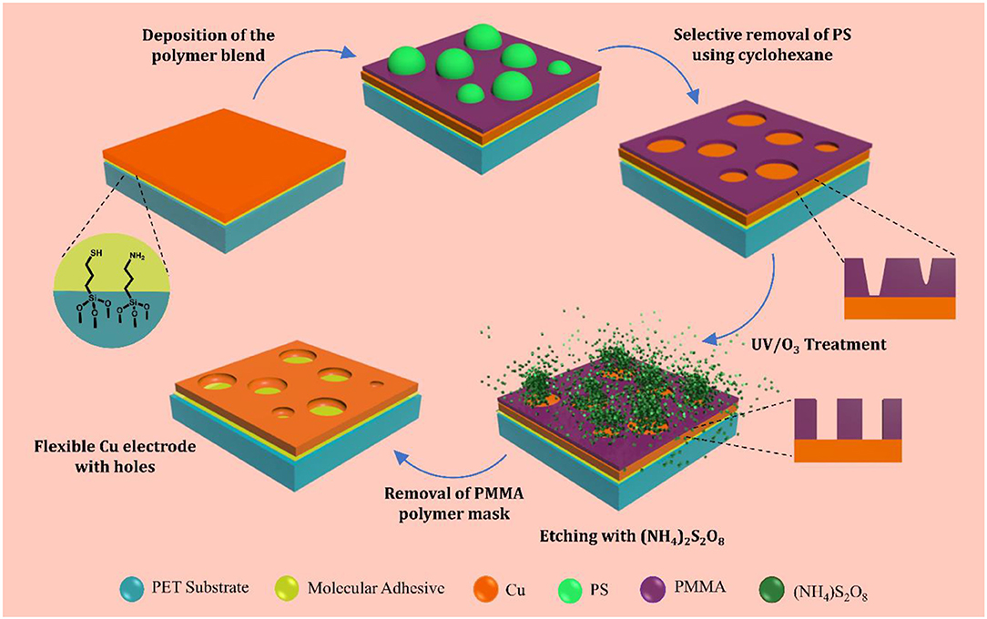
Figure 1. Schematic of electrode fabrication procedure.
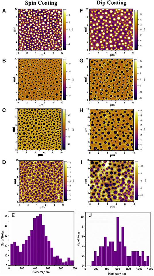
Figure 2. AFM images showing the morphology of: (A) the PS:PMMA polymer-blend (15 mg ml−1) spin cast onto an 11 nm Cu film on PET substrates, showing spherical PS islands dispersed in a PMMA matrix; (B) following the selective removal of PS using cyclohexane the peaks are transformed into holes; (C) the resulting PMMA film is UV/O3 treated to remove residual polymers within the holes and to ensure the holes extend right through the PMMA to the underlying metal; (D) ammonium persulfate etched Cu film showing circular apertures. (F–I) are representative AFM images showing the morphology of the film when the same steps are repeated following the deposition of the polymer-blend by dip coating; Histograms showing the size distribution of apertures computed for 10 × 10 μm2 AFM images of the etched Cu electrode where the PMMA mask was fabricated by spin coating (E) and dip coating (J) the PS/PMMA blend.
The primary difference between Cu electrodes fabricated using a spin cast and dip coated mask is in the density of apertures in the Cu film (Figures 2E,J): Electrodes fabricated by spin casting the resist layer have a total aperture area of 29 ± 1 vs. 25 ± 1% for electrodes fabricated using a dip coated resist layer. It is anticipated that by fine tuning of the dip coating deposition parameters it is feasible to achieve the same result using the two different methods. For convenience all of the OPV devices fabricated as part of this study were fabricated by spin coating the polymer-blend.
The AFM images in Figure 2 show that the distribution of aperture sizes using both methods is broadly similar, consistent with our previously-reported observation that the PS domain size in PS/PMMA blends is primarily determined by the solution concentration (Pereira et al., 2018). Notably, SEM imaging together with the cross-sectional AFM image (Figure S1) show that the edges of the apertures are tapered, which did not occur on glass substrates (Pereira et al., 2018). However, the AFM cross-section also shows that the hole in the Cu film is 2–5 nm deeper than the combined thickness of the metal film and the APTMS/MPTMS adhesion layer, indicating that the PET substrate has been partially etched by the acetic acid wash used to remove residual PMMA and Cu oxide from the Cu surface. The tapered edge in the film is therefore attributed to nanoscale sagging of the surrounding metal into the hole in the PET, which, whilst pronounced in the SEM image is too small to affect the macroscopic properties of the electrode. The Cu electrodes with apertures have a Tavg of 75.9% over the range of 400–800 nm (Figure 3A) with an 18.8% average increase in the total transmittance over this wavelength as compared to unpatterned Cu films of the same thickness. The absolute reduction in reflectance upon introduction of apertures increases with increasing wavelength from 5% at 400 nm to 40% at 900 nm (Figure 3B). The far-field transmittance of these perforated window electrodes is further increased to 86.4% (400–800 nm) using a ~62 nm thick ZnO overlayer (Figure S2) deposited from solution at low temperature. It is well-known that the transparency of low-loss metallic films, including Cu, can be boosted by coating with a thin high-index dielectric layer due to an effective optical path length reduction through the metal (predicted by Maxwell's equations) and reduced reflectance, and that the efficacy of this overlayer is a function of its thickness (Shakhs et al., 2016). Importantly the ZnO overlayer not only contributes to an increase in transmittance but also serves as an electron transport layer (ETL) that spans the apertures in the underlying metal substantially reducing the electrode Rsh. The introduction of apertures increases the Rsh from 8.4 ± 0.5 to 29.9 ± 1.2 Ω sq−1 because the apertures scatter electrons moving in the plane of the electrode. However, after deposition of a ZnO overlayer, which includes annealing at 145°C, the Rsh drops to 21.9 ± 1.1 Ω sq−1, and continues to fall upon storage such that after 4 months the Rsh is reduced to ~11.3 ± 1.5 Ω sq−1. We have previously shown for Cu–ZnO electrodes supported on glass that these large reductions in Rsh are due to diffusion of Cu into the ZnO overlayer, where it is believed to accumulate as metallic Cu at the boundaries between ZnO crystallites reducing the contact resistance between them and increasing the in-plane ZnO conductivity (Pereira et al., 2018). The ~50% decrease in Rsh after 4 months was accompanied by a very small (<2%) reduction in the average transmittance to Tavg = 84.6% (400–800 nm; Figure S3), although overall the Haacke FoM is increased from 0.0107 to 0.0166 Ω−1 which is substantially higher than previously achieved on glass (0.0135 Ω−1; Pereira et al., 2018; Figure S4).
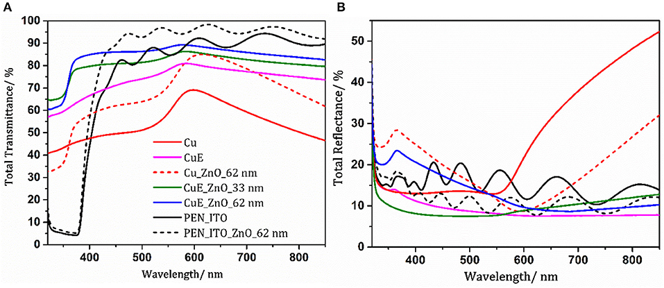
Figure 3. (A) Total far-field transparency and (B) total reflectance of 11 nm Cu films before and after the introduction of nano–apertures (CuE), and ITO coated PEN substrates with and without ZnO (referenced to bare substrate).
An essential characteristic of flexible electrodes is the ability to sustain physical deformation without significant deterioration in conductance. In order to evaluate how our Cu on PET electrodes behave upon deformation a bending test was performed in which the electrode was bent repeatedly (100 times) through a 4 mm radius of curvature. Electrodes were bent inwards (compressed) and outwards (stretched) in separate experiments. It is evident from the data in Figure 4 that there is a negligible change in Rsh for Cu electrodes with and without apertures. In contrast the Rsh of the ITO on PEN deteriorates rapidly upon repeated bending, consistent with previous reports (Alzoubi et al., 2011; Stec and Hatton, 2012). These differences in robustness can be understood in terms of the difference in the thickness of the ITO and Cu layers, and the nature of bonds between atoms comprising these conductors: The Cu thickness is more than an order of magnitude thinner than the ITO film thickness and so the stress in the Cu film upon bending is proportionally lower. Additionally, unlike the directional covalent bonds in ITO, metallic bonds are flexible, enabling moderate elastic deformation.
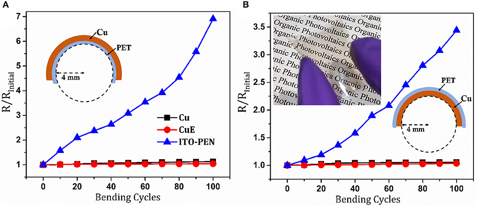
Figure 4. Change in Rsh when the Cu, CuE electrodes supported on PET and ITO coated PEN electrodes are subjected to repeated bending in the (A) outward (stretched) and (B) inward (compressed) directions. Inset: A photograph of a flexible CuE electrode with a ZnO (~62 nm) overlayer.
In order to test the applicability of these electrodes in flexible solution processed OPVs, devices were fabricated using PCE12 and m-ITIC as the donor and acceptor respectively in bulk heterojunction (BHJ) OPV devices with the architecture; Transparent electrode/ZnO (x nm)/PCE12–m-ITIC (100 nm)/MoOz (10 nm)/Ag (85 nm), where x = 25–62 nm. Whilst the highest transparency was achieved when the ZnO thickness was ~62 nm (Figure S2) this was not the optimal thickness for OPV devices. When the ZnO thickness was varied the best device performance was achieved for a ZnO thickness of ~33 nm (Table S2 and Figure S5). Transfer matrix optical simulations of the entire OPV device, with the extinction coefficient for the BHJ set to zero, confirms that more light is coupled into the device when the ZnO thickness is 33 than 62 nm: Figures S6, S7, due to optical interference effects. Using this optimal ZnO thickness a champion power conversion efficiency of 8.68% (8.25 ± 0.32%) was achieved, which to the authors' knowledge is the highest efficiency reported to date for an OPV device using a Cu based window electrode (Table S1; Jeong et al., 2018). It is evident from the external quantum efficiency (EQE) data in Figure 5B that the improvement in Jsc, as compared to the electrode without apertures, correlates with the increase in electrode transparency, being most enhanced for shorter wavelengths. Interestingly the dark current characteristics of both Cu and CuE electrodes exhibit very suppressed forward current injection in the dark, which is tentatively attributed to UV light induced oxygen desorption from ZnO which is readsorbed in the dark as this is a reversible process (Manor et al., 2012; Pereira and Hatton, 2018).
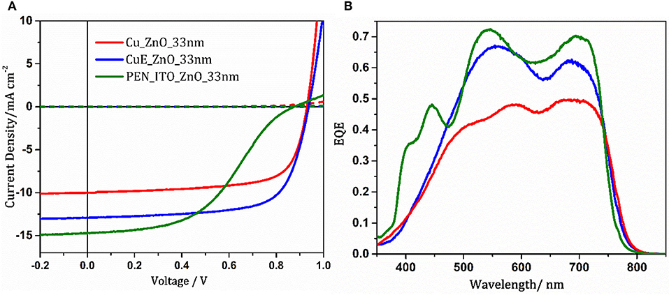
Figure 5. (A) Representative current density—voltage characteristics recorded under one sun simulated solar illumination (100 mW cm−2; AM 1.5 G) (solid lines) and in the dark (dotted lines) for devices with the architecture: Transparent electrode/ZnO (33 nm)/PCE12—m-ITIC/MoOz (10 nm)/Ag (85 nm) and (B) EQE under same conditions for devices with Cu (red) and CuE (blue) and ITO (green) electrodes.
To directly compare the performance of the Cu electrode on PET against commercial ITO coated plastic substrates, OPV devices were fabricated using ITO coated polyethylene naphthalate (PEN) as the transparent electrode (Figure 5). It is evident from Figure 5A and Table S2 that devices using the ITO electrode exhibit a higher Jsc (14.5 ± 0.2 mA cm−2) than those using the Cu electrode (12.8 ± 0.25 mA cm−2), but both the Voc and FF are much lower in the former. The larger Jsccorrelates with the higher far-field transmittance of ITO (Figure 3A) although this does not translate to a higher power conversion efficiency because the FF is significantly degraded due to an s-shaped kink, which also erodes the Voc and this behaviour was not observed when identical devices were fabricated on ITO coated glass substrates (Figure S8). An s-shaped kink in the J-V characteristic is typical of accumulation of one charge carrier type at an interface in the device (Lechêne et al., 2014). Given that both OPVs are identical except in the choice of transparent electrode, the interface in question must be that between the ITO and ZnO. Alternatively the s-shape kink may result from a local deterioration in the ITO conductivity due to deformation of the ITO layer by the spring loaded pins connecting each device to the external circuit. The origin of the s-shaped kink in the J-V characteristic is the subject of ongoing investigation, although the poor performance of inverted OPVs using ITO supported on PEN as the substrate electrode serves to highlight the inadequacy of this transparent substrate electrode for flexible OPVs.
Conclusion
In summary, we report highly transparent Cu window electrodes suitable for flexible OPVs, based on an optically-thin Cu film perforated with over 100 million sub-micron holes per square centimeter on PET with a thin ZnO over layer. These electrodes offer a far-field transmittance of 84.6% across the wavelength range 400–800 nm, with a Rsh of 11.3 ± 1.5 Ω sq−1. We have demonstrated the utility of this electrode in flexible OPV devices with a champion power conversion efficiency of ~8.7%, which is the highest reported efficiency for an OPV using a Cu based window electrode to date. We have also shown that it is possible to fabricate the polymer mask used to form apertures in the Cu film, by simple dip coating, which is a scalable deposition method compatible with roll-to-roll processing. Consequently, we see no fundamental obstacle to scaling-up the fabrication of this electrode using a continuous roll-to-roll process, since: (i) vacuum evaporation is proven as a low cost method for roll-to-roll deposition of metal films on plastic—as is evidenced by its extensive use in the food packaging industry; (ii) in principle the fabrication steps involving removal of the very thin polymer layers by solvent washing, ammonium persulfate etching of Cu, and ZnO deposition from solution, could all be achieved by dip-coating; (iii) the UV/O3 etching step could be performed rapidly in-line with an intense UV lamp and the thin ZnO film could be flash annealed.
Data Availability
All data supporting this study are provided as supplementary information accompanying this manuscript.
Author Contributions
HP designed and conducted all the experimental work, analyzed the data, and wrote the manuscript. RH conceived the study and assisted with data analysis and co-wrote the manuscript.
Conflict of Interest Statement
The authors declare that the research was conducted in the absence of any commercial or financial relationships that could be construed as a potential conflict of interest.
Acknowledgments
The authors would like to thank the United Kingdom Engineering and Physical Sciences Research Council (EPSRC) for funding (Grant number: EP/N009096/1) and the University of Warwick for the award of a Chancellor's International Scholarship to HP.
Supplementary Material
The Supplementary Material for this article can be found online at: https://www.frontiersin.org/articles/10.3389/fmats.2019.00228/full#supplementary-material
References
Alzoubi, K., Hamasha, M. M., Lu, S., and Sammakia, B. (2011). Bending fatigue study of sputtered ITO on flexible substrate. J. Disp. Technol. IEEE 7, 593–600. doi: 10.1109/JDT.2011.2151830
Burdick, G. A. (1963). Energy band structure of copper. Phys. Rev. 129, 138–150. doi: 10.1103/PhysRev.129.138
Cui, Y., Yao, H., Zhang, J., Zhang, T., Wang, Y., Hong, L., et al. (2019). Over 16% efficiency organic photovoltaic cells enabled by a chlorinated acceptor with increased open-circuit voltages. Nat. Comm. 10:2515. doi: 10.1038/s41467-019-10351-5
De Arco, L. G., Zhang, Y., Schlenker, C. W., Ryu, K., Thompson, M. E., and Zhou, C. (2010). Continuous, highly flexible, and transparent graphene films by chemical vapor deposition for organic photovoltaics. ACS Nano 4, 2865–2873. doi: 10.1021/nn901587x
Galagan, Y., Rubingh, J. E. J. M., Andriessen, R., Fan, C. C., Blom, P. W. M., Veenstra, S. C., et al. (2011). ITO-free flexible organic solar cells with printed current collecting grids. Sol. Energy Mater. Sol. Cells 95, 1339–1343. doi: 10.1016/j.solmat.2010.08.011
Garner, S. M. (2017). Flexible Glass : Enabling Thin, Lightweight, and Flexible Electronics (New York, NY), 211–246.
Haacke, G. (1976). New figure of merit for transparent conductors. J. Appl. Phys. 47, 4086–4089. doi: 10.1063/1.323240
Haacke, G. (1977). Transaprent Conducting Coaings. Annu. Rev. Mater. Sci. 7, 73–94. doi: 10.1146/annurev.ms.07.080177.000445
Hu, L., Wu, H., and Cui, Y. (2011). Metal nanogrids, nanowires, and nanofibers for transparent electrodes. MRS Bull. 36, 760–765. doi: 10.1557/mrs.2011.234
Ierides, I., Zampetti, A., and Cacialli, F. (2019). The resurgence of organic photovoltaics. Curr. Opin. Green Sustain. Chem. 17, 15–20. doi: 10.1016/j.cogsc.2018.12.004
Jeong, G., Jung, S., Choi, Y., Lee, J., Seo, J., Kim, D. S., et al. (2018). A highly robust and stable graphene-encapsulated Cu-grid hybrid transparent electrode demonstrating superior performance in organic solar cells. J. Mater. Chem. A 6, 24805–24813. doi: 10.1039/C8TA09868A
Kippelen, B., Brédas, J.-L., and Bredas, J.-L. (2009). Organic photovoltaics. Energ Env. Sci. 2, 251–261. doi: 10.1039/b812502n
Lechêne, B., Leroy, J., Tosoni, O., de Bettignies, R., and Perrier, G. (2014). Origin of the S-shape upon aging in standard organic solar cells with zinc oxide as transport layer. J. Phys. Chem. C 118, 20132–20136. doi: 10.1021/jp5051518
Lee, J., Lee, P., Lee, H., Lee, D., Lee, S. S., and Ko, S. H. (2012). Very long Ag nanowire synthesis and its application in a highly transparent, conductive and flexible metal electrode touch panel. Nanoscale 4:6408. doi: 10.1039/c2nr31254a
Manor, A., Katz, E. A., Tromholt, T., and Krebs, F. C. (2012). Enhancing functionality of ZnO hole blocking layer in organic photovoltaics. Sol. Energy Mater. Sol. Cells 98, 491–493. doi: 10.1016/j.solmat.2011.11.026
Meng, L., Zhang, Y., Wan, X., Li, C., Zhang, X., Wang, Y., et al. (2018). Organic and solution-processed tandem solar cells with 17.3% efficiency. Science 361, 1094–1098. doi: 10.1126/science.aat2612
Mohammad Bagher, A. (2014). Comparison of organic solar cells and inorganic solar cells. Int. J. Renew. Sustain. Energy 3:53. doi: 10.11648/j.ijrse.20140303.12
Naik, G. V., Shalaev, V. M., and Boltasseva, A. (2013). Alternative plasmonic materials: beyond gold and silver. Adv. Mater. 25, 3264–3294. doi: 10.1002/adma.201205076
Park, H., Chang, S., Zhou, X., Kong, J., Palacios, T., and Gradecak, S. (2015). Flexible graphene electrode-based organic photovoltaics with record-high efficiency. ECS Trans. 69, 77–82. doi: 10.1149/06914.0077ecst
Pereira, H. J., and Hatton, R. A. (2018). Copper substrate electrode for efficient top-illuminated organic photovoltaics. ACS Appl. Mater. Interfaces 11:8b18453. doi: 10.1021/acsami.8b18453
Pereira, H. J., Hutter, O. S., Dabera, G. D. M. R., Rochford, L. A., and Hatton, R. A. (2017). Copper light-catching electrodes for organic photovoltaics. Sustain. Energy Fuels 1, 859–865. doi: 10.1039/C7SE00077D
Pereira, H. J., Reed, J., Lee, J., Varagnolo, S., Dabera, G. D. R., and Hatton, R. A. (2018). Fabrication of copper window electrodes with ≈108 apertures cm−2 for organic photovoltaics. Adv. Funct. Mater. 28:1802893. doi: 10.1002/adfm.201802893
Rathmell, A. R., and Wiley, B. J. (2011). The synthesis and coating of long, thin copper nanowires to make flexible, transparent conducting films on plastic substrates. Adv. Mater. 23, 4798–4803. doi: 10.1002/adma.201102284
Shakhs, M. A., Augusto, L., Markley, L., and Chau, K. J. (2016). Boosting the transparency of thin layers by coatings of opposing susceptibility: how metals help see through dielectrics. Sci. Rep. 6:20659. doi: 10.1038/srep20659
Stec, H. M., and Hatton, R. A. (2012). Widely applicable coinage metal window electrodes on flexible polyester substrates applied to organic photovoltaics. ACS Appl. Mater. Interfaces 4, 6013–6020. doi: 10.1021/am3016763
Stoppa, M., and Chiolerio, A. (2014). Wearable electronics and smart textiles: a critical review. Sensors 14, 11957–11992. doi: 10.3390/s140711957
West, P. R., Ishii, S., Naik, G. V., Emani, N. K., Shalaev, V. M., and Boltasseva, A. (2010). Searching for better plasmonic materials. Laser Photonics Rev. 4, 795–808. doi: 10.1002/lpor.200900055
Yu, L., Shearer, C., and Shapter, J. (2016). Recent development of carbon nanotube transparent conductive films. Chem. Rev. 116, 13413–13453. doi: 10.1021/acs.chemrev.6b00179
Zamarayeva, A. M., Ostfeld, A. E., Wang, M., Duey, J. K., Deckman, I., Lechene, B., et al. (2017). Flexible and stretchable power sources for wearable electronics. Sci. Adv. 3:e1602051. doi: 10.1126/sciadv.1602051
Keywords: flexible, copper, transparent electrode, polymer-blend lithography, inverted photovoltaic devices
Citation: Pereira HJ and Hatton RA (2019) High Figure-of-Merit Transparent Copper–Zinc Oxide Window Electrodes for Organic Photovoltaics. Front. Mater. 6:228. doi: 10.3389/fmats.2019.00228
Received: 17 February 2019; Accepted: 04 September 2019;
Published: 19 September 2019.
Edited by:
Ram Gupta, Pittsburg State University, United StatesReviewed by:
Manuel Pereira Dos Santos, University of Evora, PortugalJoe Briscoe, Queen Mary University of London, United Kingdom
Sanket Datta Bhoyate, University of North Texas, United States
Camila Zequine, Pittsburg State University, United States
Copyright © 2019 Pereira and Hatton. This is an open-access article distributed under the terms of the Creative Commons Attribution License (CC BY). The use, distribution or reproduction in other forums is permitted, provided the original author(s) and the copyright owner(s) are credited and that the original publication in this journal is cited, in accordance with accepted academic practice. No use, distribution or reproduction is permitted which does not comply with these terms.
*Correspondence: Ross A. Hatton, Um9zcy5IYXR0b25Ad2Fyd2ljay5hYy51aw==