 Qian Lv
 Xiaolu Qin1†
 Ruitao Lv
- 1State Key Laboratory of New Ceramics and Fine Processing, School of Materials Science and Engineering, Tsinghua University, Beijing, China
- 2Key Laboratory of Advanced Materials (MOE), School of Materials Science and Engineering, Tsinghua University, Beijing, China
Two-dimensional metallic NbS2 has attracted increasing attentions due to its excellent properties. So far, the preparations of NbS2 are mainly focused on the mechanical exfoliation and molecular beam epitaxial (MBE), both of which have limitations, such as, small lateral sizes (usually <1 μm), low yield, etc. Chemical vapor deposition (CVD) has been used to synthesize NbS2, but mainly depends on atomically flat substrates (e.g., graphene, h-BN) to grow thinner and larger sheets and the growth of NbS2 on SiO2/Si is still challenging. In this contribution, NbS2 single crystals with different layers are controllably synthesized. Few-layer NbS2 single crystals from one layer to nine layers with several tens of micrometers lateral sizes (up to ~20 μm) can be obtained by controlling hydrogen content in Ar/H2 carrier gas, NaCl amount, the growth temperature and the growth time, which are much larger than that synthesized by the MBE route. Meanwhile, as-synthesized NbS2 demonstrates higher sensitivity for probing trace amount of molecules than that of graphene, ascribed to the efficient charge transfer between NbS2 and molecules.
Introduction
Two-dimensional (2D) transition metal dichalcogenides (TMDCs) have been widely investigated in electronic and optoelectronic fields in terms of their unique properties (Liu et al., 2013, 2016; Kim et al., 2018; Ponomarev et al., 2018; Liu H. et al., 2019; Lv and Lv, 2019; Sheng et al., 2019). Based on the bandgap structures, they can be mainly divided into two categories: (1) semiconducting and (2) metallic TMDCs. 2D semiconducting TMDCs (e.g., 2H-MoS2, 2H-MoSe2, 2H-WS2, 2H-WSe2) have been widely investigated (Chen et al., 2017; Jeong et al., 2017; Nguyen et al., 2018; Kim et al., 2019). In recent years, metallic TMDCs [e.g., niobium disulfide (NbS2)] are attracting increasing research attentions due to their unique properties, such as, charge density wave (Wang X. et al., 2018), superconductivity (Wang H. et al., 2017), magnetism (Li et al., 2018). Mechanical exfoliation (Ma et al., 2018) and molecular beam epitaxy (MBE) (Wang H. et al., 2017; Xie et al., 2018) have been used to prepare 2D NbS2. Although high-quality 2D NbS2 samples can be obtained by the mechanical exfoliation method, the yield is relatively low and not enough for the scalable preparation. For MBE method, it usually requires rigorous experimental conditions, such as, ultrahigh vacuum, specific substrates (e.g., graphene, h-BN). The lateral size of as-synthesized materials is also usually small (<1 μm) (Wang H. et al., 2017; Xie et al., 2018). Ambient pressure chemical vapor deposition (APCVD) is a facile route for the controllable synthesis of 2D materials via tuning the growth parameters. Although the growth of metallic NbS2 by APCVD has been achieved, it also mainly depends on atomically flat substrates, such as, h-BN (Zhao et al., 2016; Wang X. et al., 2017). The controllable synthesis of metallic NbS2 directly on SiO2/Si substrates with larger size and thinner thickness is still very challenging.
Developing highly efficient sensing techniques is very crucial due to the increasing needs in probing specific molecules and force, monitoring diseases (Wang T. et al., 2018; Liu J. et al., 2019; Wang et al., 2019; Xue et al., 2019). Surface enhanced Raman scattering (SERS) is an efficient and fast technique to detect trace amount of molecules or even a single molecule (Yilmaz et al., 2017; Matricardi et al., 2018; Ghopry et al., 2019). Recent years, two-dimensional materials have been widely investigated as promising SERS substrates, due to their atomically flat surface, chemical stability and bio-capability, such as, doped-graphene (Lv et al., 2012, 2014; Feng et al., 2016), WSe2 (Liu et al., 2018), MoS2 (Sun et al., 2014). Usually, the enhanced mechanism of 2D TMDCs has been explained based on chemical mechanism, in which the efficient charge transfer between SERS substrates and molecules plays an important role in the Raman scattering enhancement. Yin et al. (2017) have demonstrated that phase transition from 2H to 1T phase of MoX2 (X = S, Se) can significantly improve the SERS sensitivity, mainly ascribed to the facilitated charge transfer from the Fermi level of metallic 1T-MoX2 to the highest occupied molecular orbital (HOMO) level of the probe molecules. However, the 1T-phase MX2 (M = Mo, W) is hardly to be directly synthesized due to their higher formation energy than their semiconducting counterparts. In general, the 1T-MX2 are mainly prepared by post treatment, such as, lithium ion intercalation (Zhang et al., 2017), Ar plasma treatment (Zhu et al., 2017), laser irradiation (Jiang et al., 2018), etc., which could not obtain pure 1T phase. In contrast, the metallic nature and high surface activities of NbS2 might provide opportunities as SERS substrates. And, the SERS performance of NbS2 has not been well unveiled unveiled so far due to the challenge in obtaining large-area and high-quality samples.
Herein, we synthesized large-area NbS2 with different layers by tuning the growth parameters during CVD process. The addition of NaCl can facilitate the growth of NbS2 directly on SiO2/Si. The growth parameters, such as, the hydrogen content in the Ar/H2 carrier gas, NaCl amount, the growth temperature and the growth time, can achieve the growth of NbS2 with tunable thicknesses by changing the reaction activity, vapor pressure and reaction time of precursors. As-grown NbS2 exhibits triangular shapes and uniform contrast with the maximum lateral sizes up to ~20 μm. SERS measurements display that NbS2 exhibit excellent sensitivity for different molecules (e.g., R6G, MB, and CV) with the concentration of 5 × 10⁻⁵ M, which is higher than that of graphene and provides potential applications in sensing fields.
Experimental Section
Synthesis of Few-Layer NbS2
NbS2 was synthesized by an ambient pressure chemical vapor deposition method. Nb2O5 powder and sulfur powder were used as Nb and S precursors, respectively. NaCl was used as an extremely important assistance to decrease the melting point of Nb2O5 by forming intermediate products and further facilitate the growth of NbS2. The mixtures of Nb2O5 (~240 mg) and NaCl (~70 mg) were placed on the SiO2/Si substrate, and then moved to the center of the quartz tube reactor. Another quartz boat containing ~850 mg sulfur powders was located at the upstream and heated individually. First, the quartz tube reactor was rinsed with a high Ar flow for ~5 min. After that, the furnace was heated up to 800°C in the Ar/H2 (120/8 sccm/sccm) flow at a heating rate of 20°C/min. Meanwhile, the sulfur powder was heated up to 200°C. After maintaining at 800°C for 10 min, the furnace was cooled down to room temperature quickly. By tuning the key experimental parameters, such as the hydrogen flow (2–8 sccm) in the Ar/H2 carrier gas, the growth temperature (800°C, 840°C, 880°C), the growth time (5 min, 10 min, 15 min), and NaCl amount (60 mg, 70 mg, 80 mg) in the mixture, NbS2 samples with different layers can be obtained.
Sample Characterizations
The optical images were recorded by an Olympus microscope (BX 53 M). Scanning electron microscopy (SEM) was performed on a Hitachi SU8010 system. Transmission electron microscopy (TEM) was recorded on a FET Tecnai F30 system. Atomic force microscopy (AFM) measurement was carried out on a Bruker DektakXT system with the tapping mode.
SERS Measurements
Rhodamine 6G (R6G), methylene blue (MB) and crystal violet (CV) were used as probe molecules and dissolved in ethanol to form uniform solutions with the concentration of 5 × 10⁻⁵ M. For the SERS detection of different molecules, NbS2 grown on the SiO2/Si substrate were immersed into the above three solutions for about 30 min, respectively, followed by drying in air naturally. The samples were rinsed by ethanol for several times to remove the residual molecules. The SERS measurements were carried out on a Horiba LabRAM HR Evolution system with a 500x objective and a laser spot size of ~1 μm. The excitation wavelength for probing R6G and CV is 532 nm, while for MB is 633 nm.
Results and Discussion
The growth of NbS2 was performed under ambient pressure CVD assisted by NaCl, as shown in Schemes 1A,B shows the atomic structure of monolayer NbS2 with trigonal phase (2H) and bilayer NbS2 with rhombohedral phase (3R) at the top view and side view. The 3R phase has a staggered arrangement with the second layer in the same orientation but with an in-plane shift compared to the first layer (Zeng et al., 2019). So far, the researches on the controllable synthesis of metallic NbS2 by tuning the growth parameters are not comprehensive due to the instability of NbS2 in air and their difficult growth. (Zhou J. et al., 2018) has demonstrated that salt can assist the growth of a broad variety of 2D TMDCs materials, including binary compounds, heterostructures and alloys of TMDCs. The salt could react with the transition metal oxide precursors to form intermediate products with lower melting points, which could increase the vapor pressure of reactors and further to promote the growth of 2D TMDCs. Thereafter, salt plays an extremely important role in the synthesis of 2D TMDCs materials. However, the influence of salt content in the mixture on the growth of NbS2 has not been well-investigated in the growth of NbS2, which might influence the layer numbers or lateral sizes of NbS2 so as to better control the synthesis of NbS2. So, NbS2 grown with different Nb2O5/NaCl ratios (240:60, 240:70, 240:80 wt/wt) was investigated (Figures 1a–c). It can be seen that the salt amount mainly affect the thicknesses of NbS2. The addition of NaCl may decrease the melting point of transition metal precursor and form the intermediate products so as to facilitate the growth of NbS2 directly on SiO2/Si substrate. With increasing the NaCl amount in the mixture of Nb2O5/NaCl, the melting points of precursors can be further decreased, resulting the higher vapor pressure (Li et al., 2015). With the increased vapor pressure of precursor, NbS2 is prone to nucleate on the first grown NbS2 layer while not on the SiO2/Si, resulting in the formation of multilayer NbS2 (Yang et al., 2019). The hydrogen content in the carrier gas was also studied shown in Figures 1d–f. It can be seen that the hydrogen content could influence the lateral size and layer numbers of NbS2 triangular sheets. Occasionally, thick triangular sheets with smaller size (~5 μm) (marked by arrows in Figure 1f) can be discovered at higher hydrogen content (Ar/H2 = 120/8). When the ratio of Ar and H2 is 120:4, the lateral sizes of as-synthesized NbS2 sample become larger (up to ~10 μm), which is twice as large as those synthesized at the other two conditions. Higher hydrogen can enhance the reaction activity of chalcogenides (Huang et al., 2013), leading to an efficient reaction between Nb2O5 and S, and further enhance the nucleation density with reduced lateral size (~5 μm). Reversely, lower hydrogen will decrease the reaction activity of chalcogenides and lead to a lower growth rate of NbS2 at the same growth time. The lateral sizes of NbS2 flakes grown at higher or lower hydrogen contents in the carrier gas are relatively small. Thus, a suitable hydrogen content in the carrier gas is very essential for the growth of NbS2 with larger lateral size. Simultaneously, with the increased hydrogen content in the carrier gas, the thicknesses of NbS2 sheets are also increased. The surface morphology of as-synthesized NbS2 with different thicknesses were further characterized by scanning electron microscopy (SEM) as shown in Figure S1. Figure S1a shows the low-magnification SEM image of as-synthesized NbS2 with triangular shapes. Figures S1b–d show the high-magnification SEM images of as-synthesized NbS2 with different layer stackings. The morphology of monolayer NbS2 is characterized by the low-magnification transmission electron microscopy (TEM) and shown in Figure S2a. The corresponding selected area electron diffraction (SAED) shows the typical hexagonal patterns of NbS2 (inset of Figure S2a). Based on the intensity profile analysis in Figure S2b, the atomic spacing of as-grown NbS2 is ~0.284 nm, which is consistent with previous reports (Leng et al., 2016; Zhou X. et al., 2018).
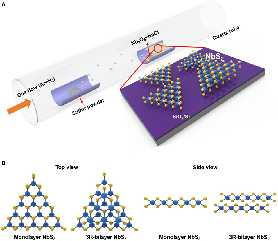
Scheme 1. (A) Illustration of the controllable growth of few-layer NbS2 by atmospheric pressure chemical vapor deposition. (B) Atomic structures of 2H-monolayer and 3R-bilayer NbS2 at the top view and side view. Yellow and blue spheres denote sulfur and niobium atoms, respectively.
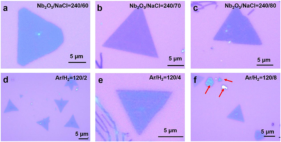
Figure 1. Growth of 2D NbS2 with different NaCl amounts and different hydrogen contents. (a–c) NbS2 grown with the Nb2O5/NaCl weight ratios of 240/60, 240/70, and 240/80, respectively. (d–f) NbS2 grown with the Ar/H2 ratios of 120/2, 120/4, and 120/8, respectively. The thicker flakes are marked by red arrows.
Figures 2a–c shows the NbS2 triangular sheets grown at different temperatures (800°C, 840°C, and 880°C). The influence of the growth temperature on the 2D materials is determined by the competition between kinetics controlled and thermodynamics controlled growth (Bogaert et al., 2016). Compared to lower growth temperature dominated by the kinetics, the higher growth temperature dominated by thermodynamics could lead to a more precursor supply and promote the growth of NbS2, so as to result in the growth of thicker NbS2 sheets with large lateral size up to ~20 μm, which is similar to the synthesis of semiconducting WSe2 grown at higher temperatures (Liu et al., 2015). The monolayer (1L) NbS2 can be obtained at 800°C. Compared to the growth temperatures, the growth time mainly affect the lateral size not the layer numbers of NbS2 as shown in Figures 2d–f, because the layer numbers are mainly related to the mass flow of precursors and growth kinetics (or thermodynamics). With the increased the growth time, the lateral sizes of NbS2 flakes are increased from ·~4–~12 μm resulted from the enough reaction time.
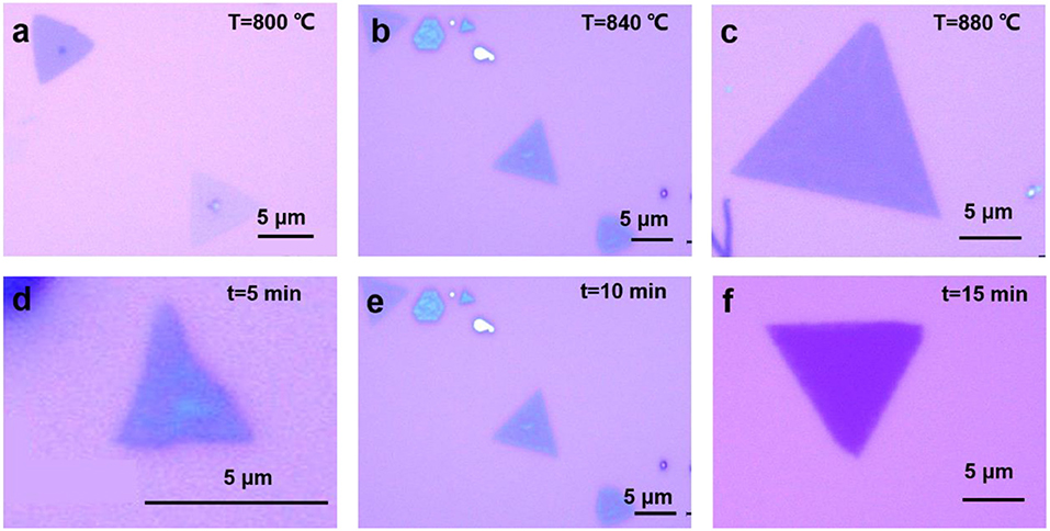
Figure 2. Growth of 2D NbS2 with different growth temperatures (T) and growth time (t). (a–c) NbS2 grown at 800, 840, and 880°C, respectively. (d–f) NbS2 grown for 5, 10, and 15 min, respectively.
The influences of above four growth parameters on the controllable growth of NbS2 can be concluded as follows. The layer numbers are mainly related to the mass flow and reaction activity of precursors and the lateral sizes are mainly related to the reaction time and reaction rate (Liu et al., 2015). NaCl can react with transition metal oxides to form intermediate products with lower melting points so as to improve the vapor pressure and increase the mass flow. The improvement of growth temperature also increases the mass flow and reaction rate of precursors. The increased hydrogen content could promote the reaction activity and reaction rate of precursor by creating reduction atmosphere. So, the amount of NaCl mainly influences the layer numbers, the growth time mainly affects the lateral sizes, but hydrogen content, and the growth temperature can both affect the layer numbers and lateral sizes of NbS2.
Monolayer NbS2 was grown at lower temperature (800°C). By increasing the growth temperature and cooperating with other growth parameters, NbS2 with different layers can be obtained. AFM was used to further verify the thicknesses as shown in Figures 3a–e. Although no atomically-flat substrate (e.g., h-BN, graphene) was used, the ultra-flat NbS2 flakes can still be obtained on the SiO2/Si substrates due to the addition of NaCl, which could decrease the formation energy of NbS2 and further promote its growth on SiO2/Si (Wang H. et al., 2017). According to the height profile shown in each AFM image, it can be seen that the thicknesses of NbS2 vary from 1.0 to 6.3 nm (Figures 3a–e), corresponding to 1L, 2L, 3L, 6L, and 9L, respectively. The relationship between the thicknesses and layer numbers is shown in Figure 3f. The crystal quality of NbS2 with various layer numbers was characterized by Raman spectra in Figure 4. All the Raman spectra are normalized to the intensity of Si peak at ~520 cm−1. Raman spectra of NbS2 show four characteristic vibration modes except for monolayer NbS2, namely, E1, E2, A1, and A2, corresponding to the unique identity of 3R-NbS2. The E2 mode and A1 mode are related to the in-plane and out-of-plane vibrations, respectively (Figure 4a). Besides, the Raman peak of NbS2 located at around 150 cm−1 might be regarded as a defect mode, which is derived from the two-phonon scattering (Ge et al., 2013). The monolayer NbS2 displays two peaks at ~304 and ~376 cm−1 marked by arrows, which are coincided with the Raman peaks of 2H NbS2 (Wang X. et al., 2017)). According to Figure 4b, it can be seen that the A1 peak blueshifts from ~376 cm−1 in monolayer to ~384 cm−1 in multilayers. The layer-dependent Raman shift demonstrates strong interactions between the layers, which might be caused by the effective restoring forces and also by the increase in dielectric screening of long-range Coulomb interactions upon adding more layers (Zhao et al., 2016; Wang X. et al., 2017). Raman mapping images of E2 and A1 peaks of bilayer NbS2 are shown in Figures 4c,d, respectively. The intensities of both peaks are evenly distributed on the triangular flake, which illustrates the uniform thickness of as-grown NbS2.
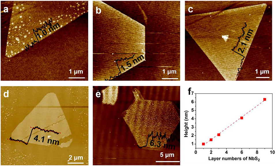
Figure 3. Atomic force microscope (AFM) of NbS2. (a–e) AFM images of NbS2 with different thicknesses. (f) The relationship between thicknesses and layers of NbS2.
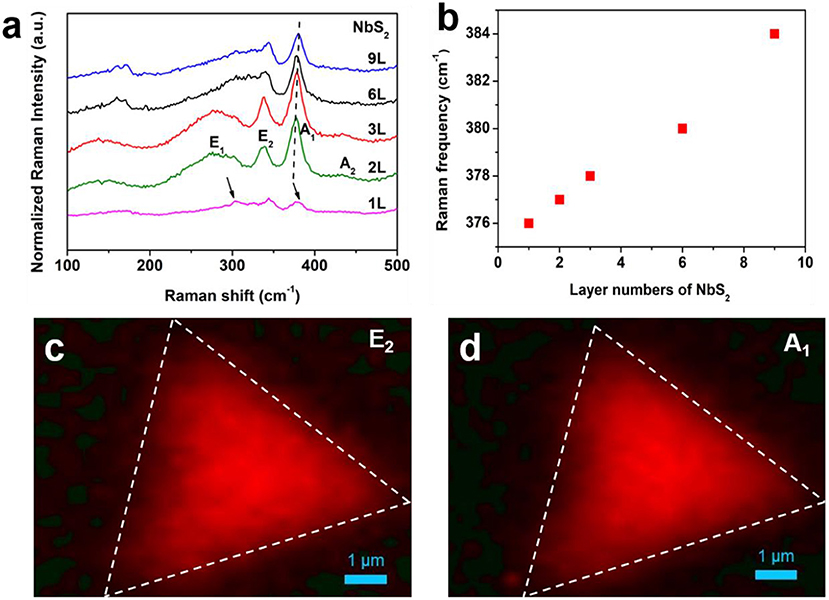
Figure 4. Raman spectra of few-layer NbS2. (a) Raman spectra of NbS2 with different layers. The characteristic peaks of monolayer NbS2 were marked by arrows. (b) Thickness-dependent Raman frequency of A1 mode of NbS2. (c–d) Raman mapping of E2 and A1 modes of bilayer NbS2.
The SERS effect of NbS2 is characterized by probing various molecules (e.g., R6G, MB and CV). Our previous studies have demonstrated that each kind of molecules has individual resonant laser excitation wavelength (Feng et al., 2016). The excitation wavelength for R6G and CV molecules is thus set as 532 nm, and for MB is 633 nm. R6G, MB and CV with the concentration of 5 × 10⁻⁵ M are utilized to evaluate the SERS performance of as-synthesized NbS2. Figure 5a illustrates the enhanced Raman scattering effect of the probe molecules coated on NbS2. After being immersed into R6G solutions and dried naturally, the Raman signals of R6G coated on NbS2 are shown in Figure 5b, demonstrating that the effective interactions between NbS2 and R6G molecules so as to induce the enhanced Raman signals of R6G coated NbS2. In addition, as-synthesized NbS2 can also probe other molecules, such as, MB and CV (Figures 5c,d), demonstrating the universality of NbS2 for sensing molecules. The characteristic peaks of R6G, MB and CV are marked by “♦,” “*,” and “♥ ,” respectively.
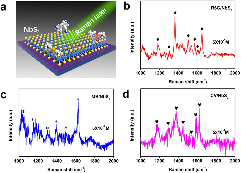
Figure 5. Surface enhanced Raman scattering (SERS) performance of as-synthesized NbS2. (a) Schematic illustration of NbS2 as SERS substrate for probing molecules. (b–d) Raman spectra of R6G, MB, and CV on NbS2, respectively. The characteristic peaks of R6G, MB and CV are marked by “♦,” “*,”and “♥ ,” respectively.
Graphene has been proven to be an efficient SERS substrates (Lv et al., 2012, 2014; Ling et al., 2014; Feng et al., 2016; Tan et al., 2017; Zhao et al., 2018). So, we conducted control experiments to compare the SERS effects of NbS2 and graphene. Graphene was synthesized by CVD as reported in our previous study (Gan et al., 2016). Raman spectrum of as-grown monolayer graphene and MoSe2 are shown in Figure S3. And, the almost negligible D mode and high I2D/IG reveal the high quality of as-grown graphene sample. R6G and MB were chosen as the probe molecules. Figure 6a displays the Raman spectra of R6G on NbS2 and graphene, respectively. The Raman signals of R6G on NbS2 are much stronger than those on graphene, which can be attributed to the more efficient charge transfer and stronger coupling between NbS2 and R6G molecules than that between graphene and R6G (Tao et al., 2018). To better compare the SERS performance of graphene and NbS2, the Raman intensities of R6G peaks at 1,362, 1,504, 1,572, and 1,650 cm−1 is shown in Figure S5a. Among the Raman intensity ratio (INbS2/IGraphene) of R6G peaks coated on NbS2 and graphene, the highest value, namely, enhancement factor, is eight times larger for NbS2 than that for graphene at ~1,360 cm−1 (Figure S5b). The Raman signals of R6G on NbS2 are also much stronger than those on MoSe2 as shown in Figure S4, which might be attributed to the more efficient charge transfer from molecules to metallic NbS2 that to semiconducting MoSe2. The Raman enhancement of MB deposited on NbS2 is slightly higher than that coated on graphene in Figure 6b. DFT calculations have demonstrated that the binding energies between NbS2 and the probe molecules are higher than those of graphene, indicating a strong coupling between NbS2 and molecules. And, the electron transfer from the probe molecules to NbS2 is also much higher than that to graphene (Song et al., 2019). Therefore, the Raman signals of molecules on NbS2 show higher intensities than those on graphene, demonstrating the much higher sensitivities of NbS2 for probing molecules. The enlarged Raman spectra of molecules on graphene are shown in Figure S6.
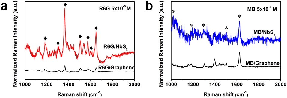
Figure 6. SERS performance comparison between as-synthesized NbS2 and monolayer graphene. (a) Raman signals of R6G on NbS2 and graphene, respectively. (b) Raman signals of MB on NbS2 and graphene, respectively. The concentrations of R6G and MB are both 5 × 10⁻⁵ M.
Understanding the SERS mechanism of metallic NbS2 is important for their potential applications. Electromagnetic enhancement (EM) and chemical enhancement are the two major mechanisms of SERS (Ghopry et al., 2019). The EM mainly depends on the localized surface plasmonic resonance (LSPR) of free charge carriers, which is the traditional SERS mechanism based on noble metal substrates with specific nanostructures, such as, Au and Ag (Matricardi et al., 2018; Li et al., 2019). And, the CM is dominated by the charge transfer between SERS substrates and molecules, which depends on the electronic structures of substrates and probe molecules. The SERS mechanism of the metallic 2D TMDCs for probing molecules has been explained by the CM, which depends on the charge transfer between TMDCs substrates and probe molecules (Yin et al., 2017; Tao et al., 2018). The efficient charge transfer between NbS2 and probe molecules might be directly related to the probing sensitivity. The charge transfer process usually includes two steps (Yin et al., 2017): First, the charges can be excited from the highest-occupied molecular orbital (HOMO) level to the lowest-unoccupied molecular orbital (LUMO) level of probing molecules, forming holes in the HOMO level. After that, the electrons could transfer from the Fermi level of NbS2 to the HOMO level of molecules, and further recombines with holes. This demonstrates that the suitable electronic structures between SERS substrates and probing molecules is essential for improving the SERS sensitivity.
Conclusions
In summary, we achieved the controllable synthesis of large-area and thickness-tunable NbS2 flakes by tuning the growth parameters during CVD process. NbS2 with different layer can be synthesized directly on SiO2/Si substrates assisted by NaCl. The NaCl amount and the growth temperature play crucial roles in the few-layer NbS2 growth by increasing the vapor pressure of precursors, while the roles of hydrogen content and the growth time in the few-layer NbS2 growth are improving the reaction activity and reaction time of precursors, respectively. The excellent SERS performance of NbS2 could provide potential applications for NbS2 in many sensing fields, such as, biosensor, chemical sensors, mechanical sensors, medical sensor, etc.
Data Availability Statement
All datasets generated for this study are included in the article/Supplementary Material.
Author Contributions
The manuscript was written through contributions of all authors. RL and QL conceived, revised the manuscript, and designed the project. XQ and QL carried out experiments, analyzed the experimental results, and wrote the manuscript. All the authors have given approval to the final version of the manuscript.
Funding
We acknowledge the financial support from the National Natural Science Foundation of China for Excellent Young Scholars (Grant No. 51722207) and the National Basic Research Program of China (Grant No. 2015CB932500). We appreciate the kindly support from Prof. Bilu Liu's group in Tsinghua-Berkeley Shenzhen Institute (TBSI) on SEM and TEM characterizations.
Conflict of Interest
The authors declare that the research was conducted in the absence of any commercial or financial relationships that could be construed as a potential conflict of interest.
Supplementary Material
The Supplementary Material for this article can be found online at: https://www.frontiersin.org/articles/10.3389/fmats.2019.00279/full#supplementary-material
References
Bogaert, K., Liu, S., Chesin, J., Titow, D., Gradecak, S., and Garaj, S. (2016). Diffusion-mediated synthesis of MoS2/WS2 lateral heterostructures. Nano Lett. 16, 5129–5134. doi: 10.1021/acs.nanolett.6b02057
Chen, J., Zhao, X., Tan, S. J., Xu, H., Wu, B., Liu, B., et al. (2017). Chemical vapor deposition of large-size monolayer MoSe2 crystals on molten glass. J. Am. Chem. Soc. 139, 1073–1076. doi: 10.1021/jacs.6b12156
Feng, S. S. M., Carvalho, B. R., Lv, R., Li, Q., Fujisawa, K., Elias, A., et al. (2016). Ultrasensitive molecular sensor using N-doped graphene through enhanced Raman scattering. Sci. Adv. 7, 1600322–1500322. doi: 10.1126/sciadv.1600322
Gan, X., Lv, R., Zhu, H., Ma, L., Wang, X., Zhang, Z., et al. (2016). Polymer-coated graphene films as anti-reflective transparent electrodes for Schottky junction solar cells. J. Mater. Chem. A 4, 13795–13802. doi: 10.1039/C6TA06261J
Ge, W., Kawahara, K., Tsuji, M., and Ago, H. (2013). Large-scale synthesis of NbS2 nanosheets with controlled orientation on graphene by ambient pressure CVD. Nanoscale 5, 5773–5778. doi: 10.1039/c3nr00723e
Ghopry, S. A., Alamri, M. A., Goul, R., Sakidja, R., and Wu, J. Z. (2019). Extraordinary sensitivity of surface-enhanced Raman spectroscopy of molecules on MoS2(WS2) nanodomes/graphene van der Waals heterostructure substrates. Adv. Optical Mater. 7, 1801249–1801259. doi: 10.1002/adom.201801249
Huang, J. P. J., Hsu, C., Chiu, M., Juang, Z., Chang, Y., Chang, W., et al. (2013). Large-area synthesis of highly rrystalline WSe2 monoLayers and device applications. ACS Nano 8, 923–930. doi: 10.1021/nn405719x
Jeong, H. Y., Jin, Y., Yun, S. J., Zhao, J., Baik, J., Keum, D. H., et al. (2017). Heterogeneous defect domains in single-crystalline hexagonal WS2. Adv. Mater. 29, 1605043–1605048. doi: 10.1002/adma.201605043
Jiang, Z., Wang, Y., Yuan, S., Shi, L., Wang, N., Xiong, J., et al. (2018). Ultrahigh-working-frequency embedded supercapacitors with 1T phase MoSe2 nanosheets for system-in-package application. Adv. Funct. Mater. 29, 1807116–1807125. doi: 10.1002/adfm.201807116
Kim, H., Yoon, Y., Ko, H., Kim, S., and Rho, H. (2019). Charge transfer across monolayer/bilayer MoS2 lateral interface and its influence on exciton and trion characteristics. 2D Mater. 6, 025004–025011. doi: 10.1088/2053-1583/aafa52
Kim, H. S., Patel, M., Kim, J., and Jeong, M. S. (2018). Growth of wafer-scale standing layers of WS2 for self-biased high-speed UV-visible-NIR optoelectronic devices. ACS Appl. Mater. Interfaces. 10, 3964–3974. doi: 10.1021/acsami.7b16397
Leng, K., Chen, Z., Zhao, X., Tang, W., Tian, B., Nai, C. T., et al. (2016). Phase restructuring in transition metal dichalcogenides for highly stable energy storage. ACS Nano 10, 9208–9215. doi: 10.1021/acsnano.6b05746
Li, J., Zhao, B., Chen, P., Wu, R., Li, B., Xia, Q., et al. (2018). Synthesis of ultrathin metallic MTe2 (M = V, Nb, Ta) single-crystalline nanoplates. Adv. Mater. 10, 1801043–1801050. doi: 10.1002/adma.201801043
Li, Q., Gong, S., Zhang, H., Huang, F., Zhang, L., and Li, S. (2019). Tailored necklace-like Ag@ZIF-8 core/shell heterostructure nanowires for high-performance plasmonic SERS detection. Chem. Eng. J. 371, 26–33. doi: 10.1016/j.cej.2019.03.236
Li, S., Wang, S., Tang, D., Zhao, W., Xu, H., Chu, L., et al. (2015). Halide-assisted atmospheric pressure growth of large WSe2 and WS2 monolayer crystals. Appl. Mater. Today 1, 60–66. doi: 10.1016/j.apmt.2015.09.001
Ling, X., Fang, W., Lee, Y. H., Araujo, P. T., Zhang, X., Rodriguez-Nieva, J. F., et al. (2014). Raman enhancement effect on two-dimensional layered materials: graphene, h-BN and MoS2. Nano Lett. 14, 3033–3040. doi: 10.1021/nl404610c
Liu, B. F. M., Chen, L., Abbas, A., Ma, Y., and Zhou, C. (2015). Chemical vapor deposition growth of monolayer WSe2 with tunable device characteristics and growth mechanism study. ACS Nano 9, 6119–6127. doi: 10.1021/acsnano.5b01301
Liu, B., Ma, Y., Zhang, A., Chen, L., Abbas, A. N., Liu, Y., et al. (2016). High-performance WSe2 field-effect transistors via controlled formation of in-plane heterojunctions. ACS Nano 10, 5153–5160. doi: 10.1021/acsnano.6b00527
Liu, H., Li, Y., Xiang, M., Zeng, H., and Shao, X. (2019). Single-layered MoS2 directly grown on rutile TiO2(110) for enhanced interfacial charge transfer. ACS Nano 13, 6083–6089. doi: 10.1021/acsnano.9b02608
Liu, J. J. X., Zhang, R., Zhang, Y., Wu, L., Lu, W., Li, J., et al. (2019). MXene-enabled electrochemical microfluidic biosensor: applications toward multicomponent continuous monitoring in whole blood. Adv. Funct. Mater. 29, 1807326–1807334. doi: 10.1002/adfm.201807326
Liu, Y., Gao, Z., Chen, M., Tan, Y., and Chen, F. (2018). Enhanced Raman scattering of CuPc films on imperfect WSe2 monolayer correlated to exciton and charge-transfer resonances. Adv. Funct. Mater. 28, 1805710–1805716. doi: 10.1002/adfm.201805710
Liu, Y., Nan, H., Wu, X., Pan, W., Wang, W., Bai, J., et al. (2013). Layer-by-layer thinning of MoS2 by plasma. ACS Nano 7, 4202–4209. doi: 10.1021/nn400644t
Lv, Q., and Lv, R. (2019). Two-dimensional heterostructures based on graphene and transition metal dichalcogenides: synthesis, transfer and applications. Carbon 145, 240–250. doi: 10.1016/j.carbon.2019.01.008
Lv, R., dos Santos, M. C., Antonelli, C., Feng, S., Fujisawa, K., Berkdemir, A., et al. (2014). Large-area Si-doped graphene: controllable synthesis and enhanced molecular sensing. Adv. Mater. 26, 7593–7599. doi: 10.1002/adma.201403537
Lv, R., Li, Q., Botello-Mendez, A. R., Hayashi, T., Wang, B., Berkdemir, A., et al. (2012). Nitrogen-doped graphene: beyond single substitution and enhanced molecular sensing. Sci. Rep. 2, 586–593. doi: 10.1038/srep00586
Ma, H., Dang, W., Yang, X., Li, B., Zhang, Z., Chen, P., et al. (2018). Chemical vapor deposition growth of single crystalline CoTe2 nanosheets with tunable thickness and electronic properties. Chem. Mater. 30, 8891–8896. doi: 10.1021/acs.chemmater.8b04069
Matricardi, C., Hanske, C., Garcia-Pomar, J. L., Langer, J., Mihi, A., and Liz-Marzan, L. M. (2018). Gold nanoparticle plasmonic superlattices as surface-enhanced Raman spectroscopy substrates. ACS Nano 12, 8531–8539. doi: 10.1021/acsnano.8b04073
Nguyen, D. A., Oh, H. M., Duong, N. T., Bang, S., Yoon, S. J., and Jeong, M. S. (2018). Highly enhanced photoresponsivity of a monolayer WSe2 photodetector with nitrogen-doped graphene quantum dots. ACS Appl. Mater. Interfaces 10, 10322–10329. doi: 10.1021/acsami.7b18419
Ponomarev, E., Pasztor, A., Waelchli, A., Scarfato, A., Ubrig, N., Renner, C., et al. (2018). Hole transport in exfoliated monolayer MoS2. ACS Nano 12, 2669–2676. doi: 10.1021/acsnano.7b08831
Sheng, Y., Chen, T., Lu, Y., Chang, R. J., Sinha, S., and Warner, J. H. (2019). High-performance WS2 monolayer light-emitting tunneling devices ssing 2D materials grown by chemical vapor deposition. ACS Nano. 13, 4530–4537. doi: 10.1021/acsnano.9b00211
Song, X., Wang, Y., Zhao, F., Li, Q., Ta, H. Q., Rummeli, M. H., et al. (2019). Plasmon-free surface-enhanced raman spectroscopy using metallic 2D materials. ACS Nano. 13, 8312–8319. doi: 10.1021/acsnano.9b03761
Sun, L., Hu, H., Zhan, D., Yan, J., Liu, L., Teguh, J. S., et al. (2014). Plasma modified MoS2 nanoflakes for surface enhanced Raman scattering. Small 10, 1090–1095. doi: 10.1002/smll.201300798
Tan, Y., Ma, L., Gao, Z., Chen, M., and Chen, F. (2017). Two-dimensional heterostructure as a platform for surface-enhanced Raman scattering. Nano Lett. 17, 2621–2626. doi: 10.1021/acs.nanolett.7b00412
Tao, L., Chen, K., Chen, Z., Cong, C., Qiu, C., Chen, J., et al. (2018). 1T' transition metal telluride atomic layers for plasmon-free SERS at femtomolar levels. J. Am. Chem. Soc. 140, 8696–8704. doi: 10.1021/jacs.8b02972
Wang, H., Huang, X., Lin, J., Cui, J., Chen, Y., Zhu, C., et al. (2017). High-quality monolayer superconductor NbSe2 grown by chemical vapour deposition. Nat Commun. 8, 394–401. doi: 10.1038/s41467-017-00427-5
Wang, T., Qi, D., Yang, H., Liu, Z., Wang, M., Leow, W. R., et al. (2019). Tactile chemomechanical transduction based on an elastic microstructured array to enhance the sensitivity of portable biosensors. Adv. Mater. 31:e1803883. doi: 10.1002/adma.201803883
Wang, T., Yang, H., Qi, D., Liu, Z., Cai, P., Zhang, H., et al. (2018). Mechano-based transductive sensing for wearable healthcare. Small 14:e1702933. doi: 10.1002/smll.201702933
Wang, X., Lin, J., Zhu, Y., Luo, C., Suenaga, K., Cai, C., et al. (2017). Chemical vapor deposition of trigonal prismatic NbS2 monolayers and 3R-polytype few-layers. Nanoscale 9, 16607–16611. doi: 10.1039/C7NR05572B
Wang, X., Liu, H., Wu, J., Lin, J., He, W., Wang, H., et al. (2018). Chemical growth of 1T-TaS2 monolayer and thin films: robust charge density wave transitions and high bolometric responsivity. Adv. Mater. 30, 1800074–1800080. doi: 10.1002/adma.201800074
Xie, S., Tu, L., Huang, L., Kang, K., Lao, K., Poddar, P., et al. (2018). Coherent, atomically thin transition-metal dichalcogenides superlattices with engineered strain. Science 359, 1131–1136. doi: 10.1126/science.aao5360
Xue, T., Liang, W., Li, Y., Sun, Y., Xiang, Y., Zhang, Y., et al. (2019). Ultrasensitive detection of miRNA with an antimonene-based surface plasmon resonance sensor. Nat. Commun. 10:28. doi: 10.1038/s41467-018-07947-8
Yang, P., Zhang, Z., Sun, M., Lin, F., Cheng, T., Shi, J., et al. (2019). Thickness tunable wedding-cake-like MoS2 flakes for high-performance optoelectronics. ACS Nano. 13, 3649–3658. doi: 10.1021/acsnano.9b00277
Yilmaz, M., Babur, E., Ozdemir, M., Gieseking, R. L., Dede, Y., Tamer, U., et al. (2017). Nanostructured organic semiconductor films for molecular detection with surface-enhanced Raman spectroscopy. Nat. Mater. 16, 918–924. doi: 10.1038/nmat4957
Yin, Y., Miao, P., Zhang, Y., Han, J., Zhang, X., Gong, Y., et al. (2017). Significantly increased Raman Enhancement on MoX2 (X = S, Se) monolayers upon phase transition. Adv. Funct. Mater. 27, 1606694–1606700. doi: 10.1002/adfm.201606694
Zeng, Z., Sun, X., Zhang, D., Zheng, W., Fan, X., He, M., et al. (2019). Controlled vapor growth and non-linear optical applications of large-area 3R phase WS2 and WSe2 atomic layers. Adv. Funct. Mater. 29, 1806874–1806881. doi: 10.1002/adfm.201806874
Zhang, J., Wu, J., Guo, H., Chen, W., Yuan, J., Martinez, U., et al. (2017). Unveiling active sites for the hydrogen evolution reaction on monolayer MoS2. Adv. Mater. 29, 1701955–1701961. doi: 10.1002/adma.201701955
Zhao, S., Hotta, T., Koretsune, T., Watanabe, K., Taniguchi, T., Sugawara, K., et al. (2016). Two-dimensional metallic NbS2: growth, optical identification and transport properties. 2D Mater. 3, 025027–025035. doi: 10.1088/2053-1583/3/2/025027
Zhao, Y., Chu, B., Zhang, L., Zhao, F., Yan, J., Li, X., et al. (2018). Constructing sensitive SERS substrate with a sandwich structure separated by single layer graphene. Sens. Actu. B Chem. 263, 634–642. doi: 10.1016/j.snb.2018.02.037
Zhou, J., Lin, J., Huang, X., Zhou, Y., Chen, Y., Xia, J., et al. (2018). A library of atomically thin metal chalcogenides. Nature. 556, 355–359. doi: 10.1038/s41586-018-0008-3
Zhou, X., Lin, S. H., Yang, X., Li, H., Hedhili, M. N., Li, L. J., et al. (2018). MoSx-coated NbS2 nanoflakes grown on glass carbon: an advanced electrocatalyst for the hydrogen evolution reaction. Nanoscale 10, 3444–3450. doi: 10.1039/C7NR09172A
Keywords: NbS2, chemical vapor deposition, controllable synthesis, charge transfer, molecular sensing
Citation: Lv Q, Qin X and Lv R (2019) Controllable Growth of Few-Layer Niobium Disulfide by Atmospheric Pressure Chemical Vapor Deposition for Molecular Sensing. Front. Mater. 6:279. doi: 10.3389/fmats.2019.00279
Received: 14 August 2019; Accepted: 21 October 2019;
Published: 06 November 2019.
Edited by:
P. Davide Cozzoli, University of Salento, ItalyReviewed by:
Dattatray Late, National Chemical Laboratory (CSIR), IndiaHan Zhang, Shenzhen University, China
Copyright © 2019 Lv, Qin and Lv. This is an open-access article distributed under the terms of the Creative Commons Attribution License (CC BY). The use, distribution or reproduction in other forums is permitted, provided the original author(s) and the copyright owner(s) are credited and that the original publication in this journal is cited, in accordance with accepted academic practice. No use, distribution or reproduction is permitted which does not comply with these terms.
*Correspondence: Ruitao Lv, bHZydWl0YW9AdHNpbmdodWEuZWR1LmNu
†These authors have contributed equally to this work