 Giulia Lucarelli
 Thomas M. Brown
- CHOSE (Centre for Hybrid and Organic Solar Energy), Department of Electronic Engineering, University of Rome Tor Vergata, Rome, Italy
Indium-doped tin oxide (ITO) is the transparent conductive material of choice for a wide range of optoelectronic devices such as sensors, light-emitting diodes, and solar cells. However, its brittle nature, high cost, scarcity as well as aggressive deposition via sputtering determine the need to find cheap alternatives with high optical transparency, low sheet resistance, and mechanical flexibility. Dielectric/metal/dielectric (D/M/D) electrodes fulfill all these requirements and are deposited via low embodied energy low-temperature processing. We developed D/M/D multilayered electrodes based on thermally evaporated MoOx or solution-processed SnO2 seed layers, a thermally evaporated ultrathin Au film, and a spin-coated SnO2 top layer on rigid glass substrates. We first systematically unraveled the role of each layer on the resistance-transmittance properties of the full D/M/D electrode structure. By optimizing the thickness of the seed, metal, and the top layer, we obtained electrodes with transmittance of 72% at 550 nm and a minimum sheet resistance of ~9 Ω sq−1. Subsequently, these optimized multilayered stacks were employed as bottom electrodes for perovskite solar cells (PSC) with glass/D/M/D/mesoporous-TiO2/CH3NH3PbI3/spiro-MeOTAD/Au device architecture, delivering power conversion efficiencies (PCE) of 10.7%. Further, we deposited and characterized D/M/D electrodes on flexible polyethylene terephthalate (PET) films, achieving a maximum PCE of 7.6%. The difference in performance compared to rigid glass devices can be ascribed to the different wetting of the active layer on PET substrates. Flexible D/M/D electrodes displayed excellent mechanical properties compared to commercial PET/ITO, showing completely stable sheet resistance after repeated bending even down to 1.5 mm of curvature radius, whereas PET/ITO showed one order of magnitude increase in sheet resistance in the same mechanical test, due to formation of cracks in the conductive oxide. Our optimized D/M/D stacks on glass and especially on PET or other types of flexible substrates are therefore excellent alternatives to ITO as transparent window electrodes for low-cost, light-weight, and conformal optoelectronics applications.
Introduction
Organic-inorganic perovskite solar cells (PSC) are on the rise as the most promising contenders among new generation photovoltaic technologies, due to the outstanding optoelectronic properties of perovskite absorbers (Correa-Baena et al., 2017) as well as associated low-cost and compatibility with large area fabrication processes (Razza et al., 2016). In the last decade, PSCs have attracted a tremendous interest in the scientific community, showing a meteoric rise in efficiency from 3.8% to the current certified record of 25.2% (https://www.nrel.gov/pv/assets/pdfs/best-research-cell-efficiencies.20190802.pdf)1 at standard test conditions. A wide range of device architectures, active layer chemical compositions, and deposition methods have been proposed for this emerging class of solar cells, in order to further boost device performance, while at the same time reducing the cost, simplifying the manufacturing processes, and improving the stability (Leijtens et al., 2017; Park, 2018). Strong efforts have also been paid to enable the fabrication of PSCs in flexible or arbitrary shapes (Di Giacomo et al., 2016) and over large-areas (Chen et al., 2018).
However, the efficiency achieved for flexible PSCs still lacks behind their rigid counterparts, with a record of 18.4% (Feng et al., 2018). This is due to the stringent process limitations imposed by plastic substrates, which suffer irreversible degradation at temperatures above 150°C (Zardetto et al., 2011), to the different wetting/growth of the perovskite active layer on flexible films (Bi C. et al., 2017), and to the generally inferior compromise between transmittance and conductance of transparent electrodes on plastic (Heo et al., 2019).
Nowadays, the most efficient PSCs are fabricated mainly on two different transparent conductive oxides (TCO): fluorine-doped tin oxide (FTO) on glass, and indium-doped tin oxide (ITO), both on glass or flexible plastic substrates. These TCOs represent a bottleneck for the low-cost fabrication of PSCs as they are obtained with energy intensive vacuum-based deposition processes. Moreover, their brittle nature (Zardetto et al., 2011; Di Giacomo et al., 2016) gains particularly significance in the context of the development of flexible PSCs: the unfavorable mechanical properties of ITO, in addition to the scarcity of indium, make the replacement of conventional TCOs with novel transparent conductive electrodes highly desirable (Kumar and Zhou, 2010). Several alternatives have been investigated to replace conventional TCOs. An optimal electrode for photovoltaic applications should be characterized by excellent optical transparency in the UV-vis-NIR range (>80%); low sheet resistance of the order of 10 Ω/sq; uniformity, conformability and flexibility; good chemical and environmental stability; low cost and easy fabrication. A smooth electrode surface is also desirable for bottom electrodes, while a certain degree of texturing is advantageous for transparent top electrodes to improve the haze (Morales-Masis et al., 2017).
Currently, the best compromise between sheet resistance and optical transparency has been achieved for electrodes based on metallic nanowires and meshes, usually based on Ag (T = 80–90%; Rs = 10–20 Ω/sq) (Li et al., 2016; Liu et al., 2017; Celle et al., 2018; Sohn et al., 2019), which are characterized by good flexibility, but usually very high roughness and poor chemical stability. Carbon-based materials like graphene have reached similar performances, but high quality can only be achieved by expensive and complex vapor-phase processes, representing an obstacle for their commercialization (Pang et al., 2011; Morales-Masis et al., 2017; La Notte et al., 2018). Carbon nanotubes (CNT) can be deposited by printing techniques but show lower electrical conductivity (Rs <100 Ω/sq, for doped CNT) (Zhou and Azumi, 2016), and high roughness. Conductive polymers such as poly(3,4-ethylenedioxythiophene) polystyrene sulfonate (PEDOT:PSS) (Vosgueritchian et al., 2012; Sun et al., 2015; Zhang et al., 2016; Hofmann et al., 2018) are widely used as low cost, solution processable alternatives, but present inferior optoelectrical properties (T ~ 80%, Rs < 100 Ω/sq).
Attractive alternatives to conventional TCOs are represented by metallic nanostructures in the form of ultrathin films (Stec et al., 2011; Zhang et al., 2017; Pereira et al., 2018) or multilayered structural configurations, such as dielectric/metal/dielectric (D/M/D), organic/metal/organic and polymer/metal/polymer architectures (Cattin et al., 2013; Della Gaspera et al., 2015; Guo et al., 2015; Aleksandrova et al., 2016; Kao et al., 2018; Liang et al., 2018). D/M/D are excellent candidates as transparent conductors (Bi et al., 2019): in general stacks based on Ag ultrathin films show the best optoelectrical properties (T = 80–90%, Rs = 10–20 Ω/sq) (Guo et al., 2012; Wang et al., 2014; Behrendt et al., 2015), but multilayers based on Au should be preferred for application in PSCs, due to their higher stability. Very high performances have been achieved for p-type stacks [for example T = 82.6%, Rs = 20.9 Ω/sq for PEDOT:PSS/Au/PEDOT:PSS (Aleksandrova et al., 2016), T = 90%, Rs = 11.5 Ω/sq for MoO3/Au/MoO3 (Della Gaspera et al., 2015)] or for ultra-thin Au films on self-assembled monolayers [T = 77%; Rs = 11 Ω/sq for MPTMS:APTMS/Au (Stec et al., 2011)].
Due to their optoelectrical and mechanical properties, D/M/D multilayered structures have been investigated as electrodes for optoelectronic devices (Kim and Lee, 2012; Kim et al., 2015; Kwon et al., 2017; Yun, 2017). Some publications are available regarding D/M/D structures as top electrodes for PSCs, such as MoOx/Au/Ag/MoOx, MoO3/Au/MoO3, MoOx/Ag/ZnS, SnOx/Ag/SnOx (Della Gaspera et al., 2015; Yang et al., 2015; Kim et al., 2016; Ou et al., 2016; Zhao et al., 2017), including a previous work from our lab (Castro-Hermosa et al., 2017), where a thermally evaporated MoOx (17.5 nm)/Au (11 nm)/MoOx (18.6 nm) top window electrode enabled the first demonstration of a PSC on opaque cellulosic paper substrate. Instead, fewer works investigated the application of D/M/D stacks as transparent bottom electrodes for PSCs. Liu et al. (2016) reported the application of WO3/Ag/WO3 electrodes fabricated by electron beam evaporation on glass and PET substrates for PSCs with an inverted device architecture; 9.7% power conversion efficiency (PCE) was achieved for rigid devices, while 8.0% was obtained for their flexible counterpart. Hu et al. (2017) developed 11.0% PSCs with a SnOx/Ag/SnOx bottom electrode where Ag was deposited by radio frequency (RF) magnetron sputtering and the SnOx by atomic layer deposition (ALD).
Here, we optimize D/M/D electrodes based on ultrathin Au films for application as bottom transparent electrodes for PSCs with a conventional n-i-p architecture. Firstly, Au was selected as the metallic layer of choice to prevent issues associated with migration of Ag in the perovskite layer, which is known to have detrimental effects on the stability of the device (Bi E. et al., 2017), as well as corrosion of Ag by migration of iodine-containing volatile compounds from the latter, that diffuse from the perovskite layer and cause the formation of AgI (Kato et al., 2015). Secondly, in order to reduce the costs associated to deposition in ultra-high vacuum and the environmental impact of the stack, we investigated, for the first time, the use of solution processed non-toxic SnO2 films to test the possibility of replacing seed layers deposited by vacuum techniques, as well as more toxic layers such as MoOx. By testing thermally evaporated MoOx and low temperature solution processed SnO2 seed layers of different thicknesses, and by optimizing the thickness of the solution processed SnO2 electron transporting/hole blocking layer, we fabricated low-cost, low-temperature manufactured electrodes with optimal combination of transmittance and sheet resistance and compatible with flexible substrates. Mechanical bending behavior of these electrodes was outstanding, showing their potential as replacement of expensive and brittle ITO. PSC on glass and PET were manufactured and differences between the two analyzed.
Materials and Methods
Materials
Molybdenum(VI) oxide (MoO3), tin chloride (SnCl2·2H2O) dehydrate, 4-tert-butylpyridine (TBP), Li-bis(trifluoromethanesulfonyl)imide (Li-TFSI), and solvents DMSO (dimethyl sulfoxide anhydrous, ≥99.9%), DMF (N,N-Dimethylformamide anhydrous, 99.8%), ethanol (99.8%), diethyl ether (99.0%) were purchased from Sigma-Aldrich. Lead (II) iodide (99.99%, trace metals basis) was purchased from TCI Deutschland GmbH. 18-NRT TiO2 paste, methylammonium iodide (CH3NH3I) and FK209 cobalt salt (98%) were purchased from Dyesol Limited. 2,2′,7,7′-tetrakis-(N,N-di-p-methoxyphenylamine)-9,9′-spirobifluorene (spiro-MeOTAD) (≥99.8%) was purchased from Borun New Material Technology Co. Ltd. D/M/D electrodes were fabricated on glass microslides (Corning®, Aldrich) or PET (Melinex®, Dupont); glass/ITO (10 Ω/sq, Kintec) and PET/ITO (12–15 Ω/sq, Flexvue) were used for reference devices.
Fabrication and Characterization of D/M/D Electrodes
MoOx/Au/SnO2 (MAS) and SnO2/Au/SnO2 (SAS) electrodes were fabricated as follows. A 0.1 M SnO2 precursor solution was prepared by dissolving SnCl2·2H2O in ethanol; after stirring overnight at room temperature, the precursor solution was spin-coated on microscope slides or PET substrates that were previously cleaned in an ultrasonic bath in soapy water, acetone (this step for glass substrates only), and isopropanol consecutively, for 15 min each. The spin-coating consisted in a double step process (1,500 rpm for 30 s, followed by 2,500 rpm for 30 s); SnO2 films were annealed at 100°C for 5 min and 150°C for 1 h in ambient air, and afterwards subdued to UV irradiation for 15 min (estimated power density 225 mW/cm2 achieved with a Dymax EC 5000 UV lamp with metal-halide bulb PN38560 and no UV-C). The spin-coating and annealing steps were repeated to achieve an increasing thickness of the oxide (a more effective strategy compared to increasing the concentration of the precursor solution). SnO2 films were transferred into a vacuum chamber and Au thermally evaporated at a pressure of 10−6 mbar and a rate of 0.03 nm/s. MoOx/Au electrodes were fabricated by thermal evaporation at 10−6 mbar, by depositing both MoOx and subsequently Au at a rate of 0.03 nm/s. The SnO2 hole blocking/electron transport layer (ETL) was deposited on top of Au as previously described for the seed layer, and the process repeated up to three times to achieve the desired thickness of the oxide. The transmittance of the electrodes was measured with a Shimadzu UV-2550 spectrophotometer. Sheet resistance (Rs) was measured with a four-point probe. The thickness of the layers was measured by using a Dektak 150 Profilometer (Bruker) and confirmed by scanning electron microscopy (SEM Leo Supra 35). Mechanical test of D/M/D structures on PET were performed by manually conforming multiple times the electrodes to cylindrical objects of different diameter, with the non-conductive side of the electrode facing the surface of the cylinders.
Device Fabrication and Characterization
PSCs were fabricated on MAS and SAS electrodes and on glass/ITO reference substrates; the latter were patterned by using a raster scanning laser (Nd:YVO4, λ = 1,064 nm, 8 ns, pulsed at 10 kHz with a fluence of 260 mJ/cm2) and cleaned in ultrasonic bath in soapy water, acetone, and isopropanol, for 15 min, respectively; before deposition of the stack, glass/ITO substrates were subdued to an UV irradiation treatment for 10 min. The solution of precursors was deposited on glass/ITO substrates as previously described in the electrode fabrication section. The TiO2 nanoparticles dispersion was prepared by diluting an 18-NRT titania paste in ethanol (1:5 w/w concentration), followed by overnight stirring at room temperature. The mesoporous layer was spin-coated at 2,500 rpm for 30 s, annealed at 150°C for 15 min and subdued to a UV-light irradiation treatment for 1.5 h, to obtain a thickness of ~250 nm. Perovskite films were deposited by a single-step solvent-engineering method in air; the solution of precursors was prepared by dissolving PbI2 and CH3NH3I (1.41 M concentration each) in DMF: DMSO 9:1 v/v mixed solvent, followed by overnight stirring at room temperature. The solution was spin-coated at 1,000 rpm for 10 s, followed by 5,000 rpm for 45 s, and 0.7 mL of diethyl ether dropped on the rotating substrates 10 s after the beginning of the second spin-coating step; perovskite films were annealed at 50°C for 2 min and then at 100°C for 10 min, obtaining an overlayer of ~350 nm on top of the TiO2 scaffold. The ~500 nm thick hole transporting layer was deposited inside a nitrogen-filled glove box by spin-coating a solution of spiro-MeOTAD [73.5 mg/mL in chlorobenzene, doped with 16.6 μL/mL LiTFSI, 26.8 μL/mL TBP, and 7.2 μL/mL Co (III) complex] at 2,000 rpm for 20 s. Finally, the 90 nm thick Au back contacts were thermally evaporated in a high vacuum chamber (10−6 mbar) through a shadow mask.
J-V curves were measured at standard test conditions (STC: AM1.5G 100 mW/cm2, 25°C), under a Class A solar simulator (ABET Sun 2000) calibrated with an EKO MS-602 pyranometer, and in the dark; current-voltage characteristics were measured with a digital source meter (Keithley 2420) by selecting a voltage step of 20 mV and a scan rate of 30 mV/s.
Results and Discussion
Optimization of Dielectric/Metal/Dielectric (D/M/D) Electrodes
We developed D/M/D electrodes based on thermally evaporated MoOx or solution processed SnO2 (i.e., seed layers), Au (i.e., conducting layer), and top SnO2 (i.e., electron extracting layer). Seed layers are required for proper growth of the conducting Au, whereas the top layer is used as electron extracting layer within the solar cell as well as antireflection layer to improve the transmittance of the D/M/D stack. We investigated the role of each layer on the optical and electrical characteristics of the composite electrodes on both PET and glass substrates.
The Role of Seed, Metal, and Top Oxide Layers and Their Combination on the Optical and Electrical Properties of Electrodes
Here, we present the effect of each layer and combination of layers of the D/M/D stack on both the transmittance and sheet resistance of the electrodes in order to determine the best option for fabricating the solar cells presented in section ITO-Free Perovskite Solar Cells Based on SnO2/Au/SnO2 and MoOx/Au/SnO2 Electrodes.
Effect of each layer on the transmittance of D/M/D electrodes
Optical transmittance of the electrode should be maximized in order to allow the incident radiation to pass through the optoelectronic device. Sandwiching the metal between two dielectric layers with a high refractive index can be a successful strategy to reduce reflectance losses of ultrathin metallic electrodes, by inducing multiple optical resonances within the dielectric layers (Zhao et al., 2015; Castro-Hermosa et al., 2017; Zhang et al., 2017). We systematically investigated the effect of both seed layers and electron-extracting layers that sandwich 10 nm thick Au, on glass and PET substrates. The results are visible in Figure 1.
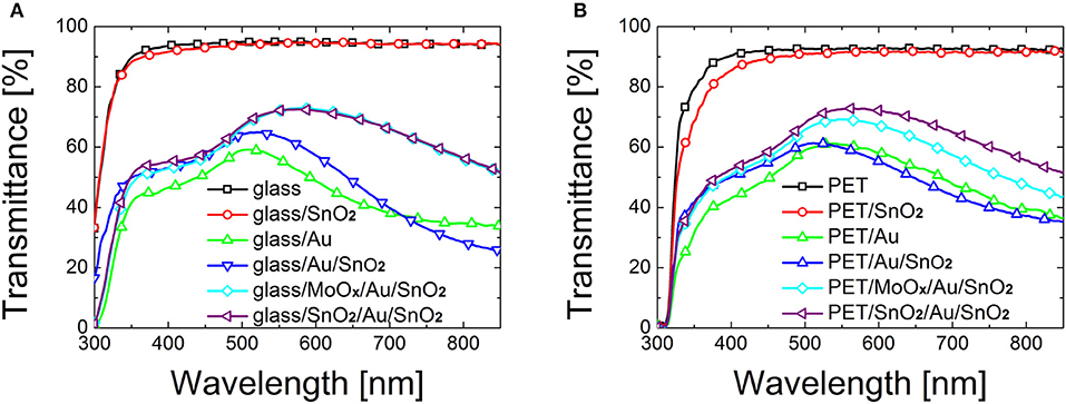
Figure 1. Transmittance of bare substrate, SnO2 (~25 nm), Au (10 nm), Au (10 nm)/SnO2 (~15 nm) bilayer, and dielectric/metal/dielectric electrodes based on SnO2 (~25 nm)/Au (10 nm)/SnO2 (~15 nm) and MoOx (18 nm)/Au (10 nm)/SnO2 (~15 nm) deposited on (A) glass and (B) PET.
The main results from Figure 1 are:
a) Evaporating Au directly on bare glass or PET is not an appropriate strategy: both average transmittance [45.05% (Tmax = 59.6%) for glass and 49.0% (Tmax = 61.8%) for PET] and sheet resistance (average 207.6 Ω/sq on glass and 82.0 Ω/sq on PET) are poor.
b) Deposition of a spin-coated SnO2 film on top of substrate/Au electrodes determines little or no improvement on the optical transmittance, with a Tave of 48.3% on glass and 49.1% on PET.
c) A remarkable improvement in transparency is observed when employing an oxide as seed layer rather than evaporating Au directly on the substrate. In particular, a 29.3% increase in Tave (Tmax = +12.4%) on glass and 16.5% increase in Tave (Tmax = +12.8%) on PET were observed when using a seed layer of MoOx under the Au layer. The addition of a SnO2 seed layer determined an increase of 30.5% in Tave (+11.8% Tmax) on glass, and a 26.3% increase in Tave (+18.8% Tmax) on PET.
Seed layers effectively improve the growth of Au by increasing the wettability of glass and PET. The mechanism of nucleation and growth can be described by addressing the surface and interfacial free energy of the metal and the oxides (Campbell, 1997): in the case of SnO2 and MoOx, the surface free energy of the metal cluster and the interfacial free energy between metal and supporting layer is lower compared to the case of bare glass and PET, therefore the 3D growth is alleviated. Moreover, a stronger adhesion of Au on the wetting layers reduces liquid-like clustering in favor of a solid-like coalescence (José-Yacamán et al., 2005), facilitating the formation of an interconnected gold network at lower amounts of metal deposited. SnO2 and MoOx seed layer-based D/M/D electrodes show comparable optical properties on glass, with a maximum transmittance of 72.6 and 73.0% respectively. A slightly higher transmittance can be observed for SnO2 based electrodes on PET compared to MoOx based electrodes (72.9% for SAS, compared to 69.2% for MAS electrodes).
Effect of each layer on the sheet resistance and stability of D/M/D electrodes
In addition to improving the transparency of the electrodes, the inclusion of a seed layer has beneficial effects on the electrical properties of the electrodes and on their stability (see Table 1).
a) One and two orders of magnitude reduction in sheet resistance was observed when including a seed layer on glass and PET substrates, respectively, bringing it down to ~9 Ω/sq.
b) Degradation of the electrodes is greatly reduced by addition of a seed layer. Sheet resistance of glass/Au/SnO2 increased by 114.8% of its initial value after 1 week storage in humid air, while electrodes with a seed layer were significantly more stable (22.7 and 34.7% increase in Rs, for SnO2 and MoOx seed layers, respectively). Smaller variations were observed for electrodes on PET (43.5% increase in Rs for seed-less electrodes, compared to a 18.1 and 22.4% for SnO2 and MoOx seed layers, respectively).
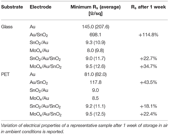
Table 1. Sheet resistance (Rs) of electrodes based on ultrathin Au films (10 nm) on glass or PET substrates; electrodes were fabricated with and without a seed layer of SnO2 (~25 nm) and MoOx (18 nm), and with and without a top SnO2 layer (~15 nm); average Rs, reported in brackets, was calculated over measurements on samples of different batches.
Seed Layer Thickness in MoOx/Au/SnO2 and SnO2/Au/SnO2 Electrodes on Glass
We tested two thicknesses of the very important seed layer (see Figure 1), either composed of thermally evaporated MoOx or solution processed SnO2. Regarding MoOx, 18 nm was theoretically and experimentally verified as the optimum by Abachi et al. (2013); 9 nm thick MoOx films lead to higher sheet resistances by ~8% in relative terms (probably due to the seed layer not being as uniform, see Supplementary Figure 1). In case of SnO2, going below 25 nm was difficult to achieve uniformly especially on PET substrates; higher thicknesses of SnO2 (~50 nm) lead to inferior results in terms of homogeneity and also lower average transparency (~12% in relative terms, see Supplementary Figure 2).
Effect of Au Thickness on the Optoelectrical Properties of the Electrodes
Figure 2 shows that the electrical and optical properties of D/M/D electrodes are very sensitive on the thickness of the metallic film sandwiched between the dielectric layers. When increasing the thickness from 5 to 10 nm, one order of magnitude reduction in sheet resistance was observed (from 120 to 9.8 Ω/sq). Instead the effect on average transmittance (range 350–850 nm) was less pronounced, with a 15% decrease in relative terms observed when increasing the thickness of Au from 5 to 10 nm.
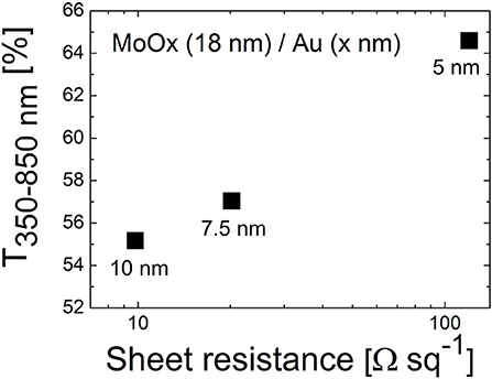
Figure 2. Average transmittance (350–850 nm) vs. sheet resistance of the dielectric/metal bilayers based on thermally evaporated MoOx (18 nm) and Au films of different thicknesses (5, 7.5, and 10 nm).
In fact, soft metals like Au grow according to a Volmer-Weber mechanism, meaning that layers form in a 3D island-like growing mode (Campbell, 1997; Zhang et al., 1997). For very thin films below a certain percolation threshold, the interconnections in the metallic nanostructure are hindered and the conductivity compromised. Below the percolation point transmittance is affected by scattering of light at the surface of metallic islands (Campbell, 1997); after the minimum thickness required for the formation of a continuous film, further increase in thickness will limit the transmission of light due to the augmented absorption caused by interaction of photons with the free electrons of the metal.
Effect of Top Oxide Layer on the Optoelectrical Properties of the Electrodes
Figure 3 shows that the optical transparency is enhanced when a top oxide layer is added to the dielectric/ultrathin metal film stack, by 16% on glass and by 20% PET. This is determined by interference and anti-reflection effects caused by the addition of a top oxide coating to a multilayer stack (Kim and Lee, 2012; Dagar et al., 2018b).
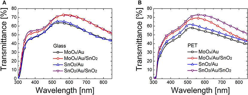
Figure 3. Transmittance of dielectric/metal and dielectric/metal/dielectric electrodes based on MoOx (18 nm)/Au (10 nm), MoOx (18 nm)/Au (10 nm)/SnO2 (~15 nm), SnO2 (~25 nm)/Au (10 nm), and SnO2 (~25 nm)/Au (10 nm)/SnO2 (~15 nm) multilayers deposited on (A) glass and (B) PET.
We also varied the thickness of the top SnO2 layer from ~15 nm, to ~25 nm, and ~35 nm. We noticed an increase in transmittance for the thicker top oxide films at wavelengths > 550 nm (see Supplementary Figure 2) which was quantified to be between 7 and 13% in relative terms in this range.
Discussion on D/M/D Electrodes for Use in Perovskite Solar Cells
Although finer control and range of thicknesses of the layers in the stack can be investigated both via optical simulations and experimentally (Kim and Lee, 2012; Abachi et al., 2013) for optimization as stand-alone electrodes, it is important to point out that priorities can change when employing them in the device of choice. When electrodes are utilized in a PSC, Dagar et al. (2018b) have shown that the optical properties of the stack are greatly modified when adding the perovskite layer over the electrode. The different multiple reflections at the new interfaces change the reflectance pattern of the sample and, for a range of wavelengths, generally let in more photons compared to a bare glass/electrode substrate (Ball et al., 2015). Therefore, greater importance should be given to optimizing the stacks for their blocking/transporting capabilities as well as quality/reproducibility upon manufacturing. The final test for electrodes lies in the manufacture of the devices.
ITO-Free Perovskite Solar Cells Based on SnO2/Au/SnO2 and MoOx/Au/SnO2 Electrodes
Perovskite Solar Cells on Glass
We fabricated complete devices on top of SAS and MAS in a mesoscopic architecture (Figure 4), since it delivers higher photocurrents and longer shelf-life stability compared to the planar one (Di Giacomo et al., 2015; Lucarelli et al., 2017) and is especially useful on PET substrates since it can be deposited a low temperature via UV-irradiation (Lucarelli et al., 2017; Dagar et al., 2018a). The complete device architecture was glass/D/M/D/m-TiO2/CH3NH3PbI3/Spiro-MeOTAD/Au.
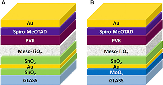
Figure 4. Schematic representation of perovskite solar cells based on dielectric/metal/dielectric electrodes with (A) ~25 nm thick SnO2 and (B) 18 nm thick MoOx seed layers, thermally evaporated Au (10 nm), and spin-coated SnO2 of variable thickness; device stack was completed with a ~250 nm thick UV-treated mesoporous TiO2 scaffold (meso-TiO2), a CH3NH3PbI3 perovskite active layer (PVK) infiltrated in the mesoporous TiO2 and forming a ~350 nm thick overlayer on top of the scaffold, a spiro-MeOTAD hole transport layer (~500 nm) and a 90 nm thick Au back electrode.
The best reference device fabricated on glass/ITO delivered a PCE of 13.6% (VOC = 1.06 V, JSC = −18.96 mA cm−2, FF = 67.4%). MAS-based PSCs performed better than the SnO2-seed layer-based counterparts, with a maximum PCE of 10.7% (VOC = 1.01 V, JSC = −17.07 mA cm−2, FF = 69.3%). SAS-based devices delivered a maximum PCE of 8.9% (VOC = 0.98 V, JSC = −14.08 mA cm−2, FF = 70.0%). The photocurrent of ITO-free PSCs was affected by the lower transmittance of D/M/D electrodes compared to glass/ITO. Statistics of the photovoltaic parameters obtained for MAS and SAS-based PSCs is reported in Supplementary Figure 3 and Supplementary Table 1, which also show that varying the thickness of the electron extracting layer does not influence appreciably the PCE. Representative J-V curves of the solar cells at STC and in the dark are shown in Supplementary Figure 4.
As reported in Table 2, the JON/JOFF ratio in the dark, where JON and JOFF are the dark current densities measured at 1 and −1 V, respectively, was roughly constant, ranging from 0.7 to 1.4 × 10² for SAS electrodes; an increase in JON/JOFF was on the other hand observed for MAS electrodes, from 0.5 × 10² of MAS1 to 0.6 × 10³ of MAS3. The rectification ratio is a fundamental parameter affecting the performance of PSCs and higher rectification currents can be a reason for the higher PCE for MAS3-based solar cells (Lucarelli et al., 2017).
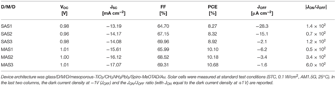
Table 2. Open circuit voltage (VOC), short circuit current (JSC), fill factor (FF), and power conversion efficiency (PCE) of the best perovskite solar cells fabricated on glass/SnO2/Au/SnO2 (SAS) and glass/MoOx/Au/SnO2 (MAS) dielectric/metal/dielectric (D/M/D) electrodes with different thickness of the SnO2 top layer, achieved by repeating the spin-coating process once (SAS1, MAS1), twice (SAS2, MAS2), or three times (SAS3, MAS3).
Maximum power point tracking (MPPT) of all devices fabricated on SAS or MAS electrodes show excellent measurement stability in time (see Supplementary Figure 5A) and limited hysteresis (hysteresis index between 10 and 20%). Shelf-life test of un-encapsulated SAS and MAS-based devices in a dry box in the dark (see Supplementary Figure 5B) shows that although degradation rates were similar, at the end of the shelf life test MAS-based devices maintain a higher efficiency, i.e., the PCE was (3.5 ± 0.9)% vs. (2.7 ± 1.2)% after 275 days considering all devices under test. MAS-PSCs deliver a higher PCE compared to SAS-based counterparts, although marginally considering standard deviations.
Perovskite Solar Cells on Flexible PET Films
Figure 5 shows the J-V curves of PET/D/M/D/m-TiO2/CH3NH3PbI3/spiro-MeOTAD/Au PSC with optimized SnO2/Au/SnO2 and MoOx/Au/SnO2 stacks on flexible PET substrates. A maximum PCE of 7.6% was achieved for PET/SAS flexible PSCs (VOC = 0.92 V, JSC = −14.09 mA cm−2, FF = 58.3%) and 5.4% for flexible PSCs on PET/MAS (VOC = 0.77 V, JSC = −11.11 mA cm−2, FF = 63.2%) and the average PCE was (5.5 ± 1.5) and (4.8 ± 0.6)%, respectively, over 4 samples.
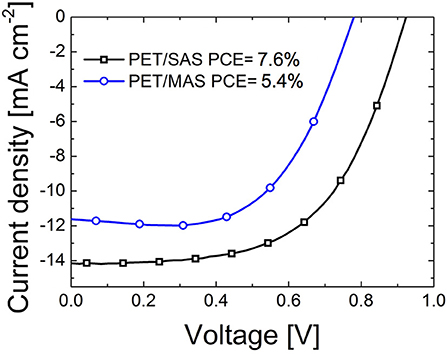
Figure 5. Current-voltage characteristics of flexible perovskite solar cells fabricated on PET/SnO2/Au/SnO2 (SAS) and PET/MoOx/Au/SnO2 (MAS) electrodes; device structure was completed with a mesoporous-TiO2/CH3NH3PbI3/spiro-MeOTAD/Au stack. Cells were measured under standard test conditions (STC, 0.1 W/cm2, AM1.5G, 25°C).
The better performance of SAS-PSCs is ascribed to a larger VOC and JSC. This is a result of higher dark JON/JOFF ratios (2.5 orders of magnitude difference between JON and JOFF, compared to 1.5 orders of magnitude for MAS-PSCs). Analyzing the microscopies of Figure 6, both PET/SAS and PET/MAS electrodes appear relatively smooth, but the latter appears to be grainer compared to the former. The better homogeneity/coverage of SAS electrodes is beneficial for fabricating compact electron-extracting layers that need to be pin-hole free. Figure 6 also shows that on glass substrates the description is inverted compared to the PET case. In fact, the homogeneity seems better for MAS electrodes compared to SAS electrodes which can explain the better initial PCE of solar cells manufactured on the former. Different surface chemistry, planarity, and wetting properties between PET and glass lead to different growth of the electrodes and of the overlaying perovskite semiconductor affecting the performances of the complete devices.
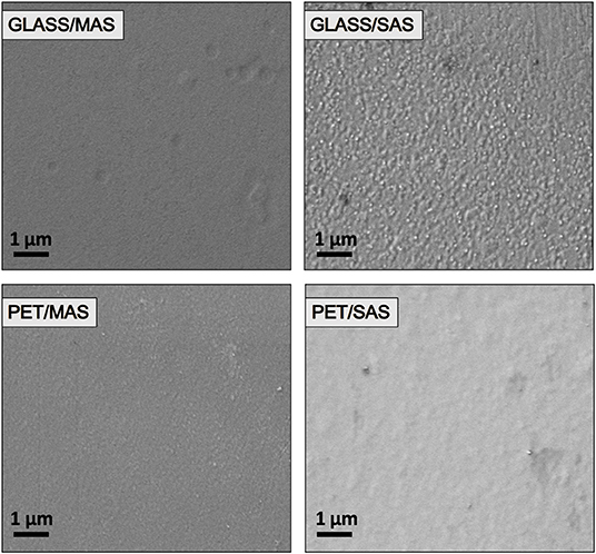
Figure 6. Scanning electron microscopy (SEM) images of MoOx (18 nm)/Au (10 nm)/SnO2 (~15 nm), labeled as MAS, and SnO2 (~25 nm)/Au (10 nm)/SnO2 (~15 nm), labeled as SAS, electrodes on glass and PET substrates; the scale is 1 μm.
Bendability of the D/M/D Electrodes
We examined the variation of sheet resistance of PET/ITO, PET/MAS, and PET/SAS by bending the electrodes (tensile stress) for 50 times at radii from 30 to 1.5 mm. As shown in Figure 7, PET/ITO showed a dramatic increase in sheet resistance, of around one order of magnitude, after bending at 5 mm curvature radius: this is due to the formation of multiple cracks in the brittle ITO layer (Zardetto et al., 2011). Remarkably, SAS and MAS electrodes on PET maintained unvaried their electrical properties after 50 bending cycles at several curvature radii, even down to a very small 1.5 mm bending radius. Thus, these D/M/D electrodes show outstanding flexibility which surpasses greatly that of ITO. Figure 8 shows the safe bending diameters for PET/ITO electrodes and D/M/D electrodes as well as cross sectional images for PSC fabricated on the former (Lucarelli et al., 2017) and the D/M/D electrodes of this work. Note, the ultrathin nature (~50 nm total thickness) of the D/M/D electrode compared to the much thicker ITO (~300 nm) electrode on PET substrate which contributes greatly to the flexibility of such a layer.
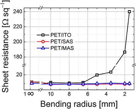
Figure 7. Sheet resistance of PET/ITO, PET/SnO2 (~25 nm)/Au (10 nm)/SnO2 (~15 nm) (SAS) and PET/MoOx(18 nm)/Au (10 nm)/SnO2 (~15 nm) (MAS) electrodes after cyclic bending (50 times, tensile stress) at several curvature radii; bending was achieved by conforming the electrodes to cylinders of known diameter, with the non-conductive side in contact with the cylinders.
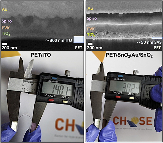
Figure 8. (Above) SEM images of a full device stack fabricated on top of PET/ITO (Lucarelli et al., 2017) and PET/SnO2/Au/SnO2 (this work), showing that D/M/D electrodes are ultrathin (~50 nm) as compared to ITO (~300 nm). (Below) Bending of PET/ITO and PET/SnO2/Au/SnO2 electrodes, with the former bended down to a safe radius of 7 mm (diameter of 14 mm), and the latter down to 1.5 mm curvature radius (diameter of 3 mm).
Conclusions
D/M/D multilayers are optimal candidates for replacing brittle and expensive ITO, as they combine low cost, excellent mechanical properties and compatibility with low-temperature large-area fabrication. Several architectures have been studied and optimized to achieve the optimal compromise between optical transparency and electrical conductivity; however, works currently available on D/M/D stacks often concern ultrathin metal films sandwiched between oxides that are deposited by energy intensive/expensive techniques, such as ALD or sputtering. We developed electrodes based on SnO2 or MoOx seed layers in combination with an ultrathin Au film and a SnO2 top oxide: while MoOx layers are deposited by thermal evaporation, SnO2 films are non-toxic alternatives that can be fabricated at low temperatures via easy solution processing. By systematically optimizing the thickness of SnO2 and MoOx seed layers, of the Au film and of the SnO2 top oxide, we developed SnO2/Au/SnO2 electrodes with maximum transmittance of 72.6% and sheet resistance as low as 9 Ω/sq on glass (72.9% and 9.2 Ω/sq on PET) and MoOx/Au/SnO2 stacks with 73% maximum transmittance and minimum sheet resistance of 9.5 Ω/sq (69.2% and 9.5 Ω/sq on PET).
Optimized multilayered structures were tested as bottom electrodes for rigid perovskite solar cells with glass/D/M/D/m-TiO2/CH3NH3PbI3/Spiro-MeOTAD/Au architecture; by tuning the thickness of the SnO2 top oxide, acting as an electron transporting/hole blocking layer, we achieved a maximum PCE of 10.7% (VOC = 1.01 V, JSC = −17.07 mA cm−2, FF = 69.31%) on glass/MoOx/Au/SnO2, and 8.9% on glass/SnO2/Au/SnO2 (VOC = 0.98 V, JSC = −14.08 mA cm−2, FF = 69.96%). In light of the good optoelectrical properties achieved for D/M/D electrodes also on PET, we transferred our optimized stacks to flexible substrates and demonstrated their application in flexible PSCs. A maximum PCE of 7.6% (VOC = 0.923 V, JSC = −14.09 mA cm−2, FF = 58.29%) was obtained for a flexible solar cell fabricated on PET/SnO2/Au/SnO2 electrodes, while a 5.4% PCE (VOC = 0.77 V, JSC = −11.11 mA cm−2, FF = 63.18%) was achieved on PET/MoOx/Au/SnO2.
The excellent mechanical properties of the electrodes were confirmed by repeated bending at several radii of curvature: whilst commercial PET/ITO showed irreversible degradation of sheet resistance after cyclic curvature at radii of 5 mm (safe bending radius of 7 mm), our optimized D/M/D electrodes on PET maintained remarkably stable electrical properties after being repeatedly flexed at bending radii as low as 1.5 mm.
ITO is currently the electrode of choice for a wide range of optoelectronic applications, such as solar cells, photodetectors and light emitting diodes. However, the brittle nature of ITO, together with its high cost, energy intensive fabrication processes, and the scarcity of indium, determine the need to find cheap alternatives with comparable optoelectrical properties. Our optimized SnO2/Au/SnO2 and MoOx/Au/SnO2 electrodes show competitive optoelectrical properties, are characterized by high bendability when fabricated on flexible PET substrates as summarized in Table 3, and can be fabricated by low temperature thermal evaporation combined with easy solution processing, therefore showing great potential as electrodes for ITO-free optoelectronic applications.
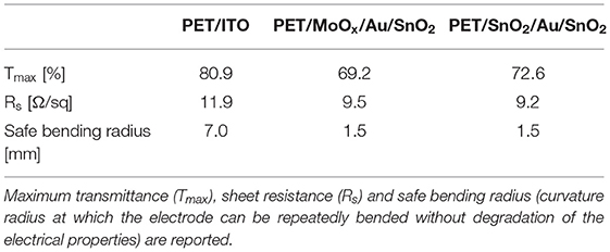
Table 3. Optoelectrical and mechanical properties of commercial PET/ITO and flexible PET/dielectric/metal/dielectric electrodes optimized in this work.
Data Availability Statement
The raw data supporting the conclusions of this manuscript will be made available by the authors, without undue reservation, to any qualified researcher.
Author Contributions
GL designed, fabricated, and characterized dielectric/metal/dielectric electrodes and perovskite solar cells and wrote the manuscript. TB envisioned and supervised the experiments and writing of the article.
Funding
This project has received funding from the European Union's Horizon 2020 research and innovation programme under Grant Agreement No. 763989 APOLO, and from the Italian Space Agency (ASI) project, PEROSKY-Perovskite and other printable materials for energy application in space (no. 2018-1-R.0). Authors also acknowledge the European H2020 project, Wearable Applications enabled by electronic Systems on Paper (WASP) (no. 825213).
Disclaimer
The article reflects the views of the authors and the funding agencies are not responsible for any use that may be made of the information that it contains.
Conflict of Interest
The authors declare that the research was conducted in the absence of any commercial or financial relationships that could be construed as a potential conflict of interest.
Acknowledgments
Authors thank Prof. Ross Hatton for useful discussion regarding the optimization of dielectric-metal-dielectric electrodes and Dr. Sergio Castro-Hermosa for sharing his expertise on the fabrication and characterization of electrodes and perovskite solar cells.
Supplementary Material
The Supplementary Material for this article can be found online at: https://www.frontiersin.org/articles/10.3389/fmats.2019.00310/full#supplementary-material
Footnotes
References
Abachi, T., Cattin, L., Louarn, G., Lare, Y., Bou, A., Makha, M., et al. (2013). Highly flexible, conductive and transparent MoO3/Ag/MoO3 multilayer electrode for organic photovoltaic cells. Thin. Solid Films 545, 438–444. doi: 10.1016/j.tsf.2013.07.048
Aleksandrova, M., Videkov, V., Ivanova, R., Singh, A. K., and Thool, G. S. (2016). Highly flexible, conductive and transparent PEDOT:PSS/Au/PEDOT:PSS multilayer electrode for optoelectronic devices. Mater. Lett. 174, 204–208. doi: 10.1016/j.matlet.2016.03.127
Ball, J. M., Stranks, S. D., Horantner, M. T., Huttner, S., Zhang, W., and Crossland, E. J. W. (2015). Optical properties and limiting photocurrent of thin-film perovskite solar cells. Energy Environ. Sci. 8, 602–609. doi: 10.1039/C4EE03224A
Behrendt, A., Friedenberger, C., Gahlmann, T., Trost, S., Becker, T., Zilberberg, K., et al. (2015). Highly robust transparent and conductive gas diffusion barriers based on tin oxide. Adv. Mater. 27, 5961–5967. doi: 10.1002/adma.201502973
Bi, C., Chen, B., Wei, H., DeLuca, S., and Huang, J. (2017). Efficient flexible solar cell based on composition-tailored hybrid perovskite. Adv. Mater. 29:160900. doi: 10.1002/adma.201605900
Bi, E., Chen, H., Xie, F., Wu, Y., Chen, W., Su, Y., et al. (2017). Diffusion engineering of ions and charge carriers for stable efficient perovskite solar cells. Nat. Commun. 8:15330. doi: 10.1038/ncomms15330
Bi, Y. -G., Liu, Y. -F., Zhang, X. -L., Yin, D., Wang, W. -Q., Feng, J., et al. (2019). Ultrathin metal films as transparent electrode in ITO-free organic optoelectronic devices. Adv. Optical Mater. 7:1800778. doi: 10.1002/adom.201800778
Campbell, C. T. (1997). Ultrathin metal films and particles on oxide surfaces. Surf. Sci. Rep. 27, 1–111. doi: 10.1016/S0167-5729(96)00011-8
Castro-Hermosa, S., Dagar, J., Marsella, A., and Brown, T. M. (2017). Perovskite solar cells on paper and the role of substrates and electrodes on performance. IEEE Elect. Device Lett. 38, 1278–1281. doi: 10.1109/LED.2017.2735178
Cattin, L., Bernède, J. C., and Morsli, M. (2013). Toward indium-free optoelectronic devices: dielectric/metal/dielectric alternative transparent conductive electrode in organic photovoltaic cells. Phys. Status Solidi Appl. Mater. Sci. 210, 1047–1061. doi: 10.1002/pssa.201228089
Celle, C., Cabos, A., Fontecave, T., Laguitton, B., Benayad, A., Guettaz, L., et al. (2018). Oxidation of copper nanowire based transparent electrodes in ambient conditions and their stabilization by encapsulation: application to transparent film heaters. Nanotechnology 29:085701. doi: 10.1088/1361-6528/aaa48e
Chen, Y., Zhang, L., Zhang, Y., Gao, H., and Yan, H. (2018). Large-area perovskite solar cells-a review of recent progress and issues. RSC Adv. 8, 10489–10508. doi: 10.1039/C8RA00384J
Correa-Baena, J.-P., Abate, A., Saliba, M., Tress, W., Jacobsson, J., Grätzel, M., et al. (2017). The rapid evolution of highly efficient perovskite solar cells. Energy Environ. Sci. 10, 710–727. doi: 10.1039/C6EE03397K
Dagar, J., Castro-Hermosa, S., Gasbarri, M., Palma, A. L., Cinà, L., Matteocci, F., et al. (2018a). Efficient fully laser-patterned flexible perovskite modules and solar cells based on low-temperature solution-processed SnO2/mesoporous-TiO2 electron transport layers. Nano Res. 11, 2669–2681. doi: 10.1007/s12274-017-1896-5
Dagar, J., Castro-Hermosa, S., Lucarelli, G., Cacialli, F., and Brown, T. M. (2018b). Highly efficient perovskite solar cells for light harvesting under indoor illumination via solution processed SnO2/MgO composite electron transport layers. Nano Energy 49, 290–299. doi: 10.1016/j.nanoen.2018.04.027
Della Gaspera, E., Peng, Y., Hou, Q., Spiccia, L., Bach, U., Jasieniak, J. H., et al. (2015). Ultra-thin high efficiency semitransparent perovskite solar cells. Nano Energy 13, 249–257. doi: 10.1016/j.nanoen.2015.02.028
Di Giacomo, F., Fakharuddin, A., Jose, R., and Brown, T. M. (2016). Progress, challenges and perspectives in flexible perovskite solar cells. Energy Environ. Sci. 9, 3007–3035. doi: 10.1039/C6EE01137C
Di Giacomo, F., Zardetto, V., D'Epifanio, A., Pescetelli, S., Matteocci, F., Razza, S., et al. (2015). Flexible perovskite photovoltaic modules and solar cells based on atomic layer deposited compact layers and UV-irradiated TiO2 scaffolds on plastic substrates. Adv. Energy Mater. 5:1401808. doi: 10.1002/aenm.201401808
Feng, J., Zhu, X., Yang, Z., Zhang, X., Niu, J., Wang, Z., et al. (2018). Record efficiency stable perovskite solar cell using effective additive assistant strategy. Adv. Mater. 30:1801418. doi: 10.1002/adma.201801418
Guo, X., Lin, J., Chen, H., Zhang, X., Fan, Y., Luo, J., et al. (2012). Ultrathin and efficient flexible polymer photovoltaic cells based on stable indium-free multilayer transparent electrodes. Mater. Chem. 22, 17176–17182. doi: 10.1039/c2jm33594h
Guo, X., Liu, X., Lin, F., Li, H., Fan, H., and Zhang, N. (2015). Highly conductive transparent organic electrodes with multilayer structures for rigid and flexible optoelectronics. Sci. Rep. 5:10569. doi: 10.1038/srep10569
Heo, J. H., Lee, D. S., Shin, D. H., and Im, S. H. (2019). Recent advancements in and perspectives on flexible hybrid perovskite solar cells. J. Mater. Chem. A 7, 888–900. doi: 10.1039/C8TA09452G
Hofmann, A. I., Cloutet, E., and Hadziioannou, G. (2018). Materials for transparent electrodes: from metal oxides to organic alternatives. Adv. Electron. Mater. 4:1700412. doi: 10.1002/aelm.201700412
Hu, T., Becker, T., Pourdavoud, N., Zhao, J., Brinkmann, K. O., Heiderhoff, R., et al. (2017). Indium-free perovskite solar cells enabled by impermeable tin-oxide electron extraction layers. Adv. Mater. 29:1606656. doi: 10.1002/adma.201606656
José-Yacamán, M., Gutierrez-Wing, C., Miki, M., Yang, D. Q., Piyakis, K. N., and Sacher, E. (2005). Surface diffusion and coalescence of mobile metal nanoparticles. J. Phys. Chem. B 109, 9703–9711. doi: 10.1021/jp0509459
Kao, P. C., Hsieh, C. J., Chen, Z. H., and Chen, S. H. (2018). Improvement of MoO3/Ag/MoO3multilayer transparent electrodes for organic solar cells by using UV–ozone treated MoO3 layer. Sol. Energy Mater. Sol. Cells 186, 131–141. doi: 10.1016/j.solmat.2018.06.031
Kato, Y., Ono, L. K., Lee, M. V., Wang, S., Raga, S. R., and Qi, Y. (2015). Silver iodide formation in methyl ammonium lead iodide perovskite solar cells with silver top electrodes. Adv. Mater. Interfaces 2:1500195. doi: 10.1002/admi.201500195
Kim, H., Kim, H. S., Ha, J., Park, N. G., and Yoo, S. (2016). Empowering semi-transparent solar cells with thermal-mirror functionality. Adv. Energy Mater. 6:1502466. doi: 10.1002/aenm.201502466
Kim, J. H., Lee, J. H., Kim, S. -W., Yoo, Y. -Z., and Seong, T. -Y. (2015). Highly flexible ZnO/Ag/ZnO conducting electrode for organic photonic devices. Ceram. Int. 41, 7146–7150. doi: 10.1016/j.ceramint.2015.02.031
Kim, S., and Lee, J.-L. (2012). Design of dielectric/metal/dielectric transparent electrodes for flexible electronics. J. Photon. Energy 2:021215. doi: 10.1117/1.JPE.2.021215
Kumar, A., and Zhou, C. (2010). The race to replace tin-doped indium oxide: which material will win? ACS Nano 4, 11–14. doi: 10.1021/nn901903b
Kwon, J. H., Choi, S., Jeon, Y., Kim, H., Chang, K. S., and Choi, K. C. (2017). Functional design of dielectric-metal-dielectric-based thin-film encapsulation with heat transfer and flexibility for flexible displays. ACS Appl. Mater. Interfaces 9, 27062–27072. doi: 10.1021/acsami.7b06076
La Notte, L., Bianco, G. V., Palma, A. L., Di Carlo, A., Bruno, G., and Reale, A. (2018). Sprayed organic photovoltaic cells and mini-modules based on chemical vapor deposited graphene as transparent conductive electrode. Carbon 129, 878–883. doi: 10.1016/j.carbon.2017.08.001
Leijtens, T., Bush, K., Cheacharoen, R., Beal, R., Bowring, A., and McGehee, M. D. (2017). Towards enabling stable lead halide perovskite solar cells; interplay between structural, environmental, and thermal stability. J. Mater. Chem. A 5, 11483–11500. doi: 10.1039/C7TA00434F
Li, Y., Meng, L., Yang, Y., Xu, G., Hong, Z., Chen, Q., et al. (2016). High-efficiency robust perovskite solar cells on ultrathin flexible substrates. Nat. Commun. 7:10214. doi: 10.1038/ncomms10214
Liang, F., Lin, Y., He, Z., Chen, W., Zhu, Y., Chen, T., et al. (2018). Promising ITO-free perovskite solar cells with WO3-Ag-SnO2 as transparent conductive oxide. J. Mater. Chem. A 6, 19330–19337. doi: 10.1039/C8TA08287A
Liu, T., Liu, W., Zhu, Y., Wang, S., Wu, G., and Chen, H. (2017). All solution processed perovskite solar cells with Ag@Au nanowires as top electrode. Sol. Energy Mater. Sol. Cells 171, 43–49. doi: 10.1016/j.solmat.2017.06.025
Liu, X., Guo, X., Gan, Z., Zhang, N., and Liu, X. (2016). Efficient perovskite solar cells based on multilayer transparent electrodes through morphology control. J. Phys. Chem. C 120, 26703–26709. doi: 10.1021/acs.jpcc.6b10288
Lucarelli, G., Di Giacomo, F., Zardetto, V., Creatore, M., and Brown, T. M. (2017). Efficient light harvesting from flexible perovskite solar cells under indoor white light-emitting diode illumination. Nano Res. 10, 2130–2145. doi: 10.1007/s12274-016-1402-5
Morales-Masis, M., De Wolf, S., Woods-Robinson, R., Ager, J. W., and Ballif, C. (2017). Transparent electrodes for efficient optoelectronics. Adv. Electron. Mater. 3:16000529. doi: 10.1002/aelm.201600529
Ou, X. L., Xu, M., Feng, J., and Sun, H. B. (2016). Flexible and efficient ITO-free semitransparent perovskite solar cells. Sol. Energy Mater. Sol. Cells 157, 660–665. doi: 10.1016/j.solmat.2016.07.010
Pang, S., Hernandez, Y., Feng, X., and Müllen, K. (2011). Graphene as transparent electrode material for organic electronics. Adv. Mater. 23, 2779–2795. doi: 10.1002/adma.201100304
Park, N.-G. (2018). Morphological and compositional progress in halide perovskite solar cells. Chem. Commun. 55, 1192–1200. doi: 10.1039/C8CC08653B
Pereira, H. J., Reed, J., Lee, J., Varagnolo, S., Dabera, G. D. R., and Hatton, R. A. (2018). Fabrication of copper window electrodes with ≈108 apertures cm−2 for organic photovoltaics. Adv. Funct. Mater. 28:1802893. doi: 10.1002/adfm.201802893
Razza, S., Castro-Hermosa, S., Di Carlo, A., and Brown, T. M. (2016). Research update: large-area deposition, coating, printing, and processing techniques for the upscaling of perovskite solar cell technology. APL Mater. 4:2016. doi: 10.1063/1.4962478
Sohn, H., Park, C., Oh, J. -M., Kang, S. W., and Kim, M. -J. (2019). Silver nanowire networks: mechano-electric properties and applications. Materials 12:2526. doi: 10.3390/ma12162526
Stec, H. M., Williams, R. J., Jones, T. S., and Hatton, R. A. (2011). Ultrathin transparent Au electrodes for organic photovoltaics fabricated using a mixed mono-molecular nucleation layer. Adv. Funct. Mater. 21, 1709–1716. doi: 10.1002/adfm.201002021
Sun, K., Li, P., Xia, Y., Chang, J., and Ouyang, J. (2015). Transparent conductive oxide-free perovskite solar cells with PEDOT:PSS as transparent electrode. ACS Appl. Mater. Interfaces 7, 15314–15320. doi: 10.1021/acsami.5b03171
Vosgueritchian, M., Lipomi, D. J., and Bao, Z. (2012). Highly conductive and transparent PEDOT:PSS films with a fluorosurfactant for stretchable and flexible transparent electrodes. Adv. Funct. Mater. 22, 421–428. doi: 10.1002/adfm.201101775
Wang, W., Song, M., Bae, T. S., Park, Y. H., Kang, Y. C., Lee, S. G., et al. (2014). Transparent ultrathin oxygen-doped silver electrodes for flexible organic solar cells. Adv. Funct. Mater. 24, 1551–1561. doi: 10.1002/adfm.201301359
Yang, Y., Chen, Q., Hsieh, Y. -T., Song, T. -B., De Marco, N., Zhou, H., et al. (2015). Multilayer transparent top electrode for solution processed perovskite/Cu(In,Ga)(Se,S)2 four terminal tandem solar cells. ACS Nano 9, 7714–7721. doi: 10.1021/acsnano.5b03189
Yun, J. (2017). Ultrathin metal films for transparent electrodes of flexible optoelectronic devices. Adv. Funct. Mater. 27:1606641. doi: 10.1002/adfm.201606641
Zardetto, V., Brown, T. M., Reale, A., and Di Carlo, A. (2011). Substrates for flexible electronics: a practical investigation on the electrical, film flexibility, optical, temperature, and solvent resistance properties. J. Polym. Sci. Part B Polym. Phys. 49, 638–648. doi: 10.1002/polb.22227
Zhang, C., Kinsey, N., Chen, L., Ji, C., Xu, M., Ferrera, M., et al. (2017). High-performance doped silver films: overcoming fundamental material limits for nanophotonic applications. Adv. Mater. 29:1605177. doi: 10.1002/adma.201605177
Zhang, L., Persaud, R., and Madey, T. E. (1997). Ultrathin metal films on a metal oxide surface: growth of Au on TiO2 (110). Phys. Rev. B 56, 10549–10557. doi: 10.1103/PhysRevB.56.10549
Zhang, X., Wu, J., Wang, J., Zhang, J., Yang, Q., Fu, Y., et al. (2016). Highly conductive PEDOT:PSS transparent electrode prepared by a post-spin-rinsing method for efficient ITO-free polymer solar cells. Sol. Energy Mater. Sol. Cells 144, 143–149. doi: 10.1016/j.solmat.2015.08.039
Zhao, D., Zhang, C., Kim, H., and Guo, L. J. (2015). High-performance Ta2O5/Al-doped Ag electrode for resonant light harvesting in efficient organic solar cells. Adv. Energy Mater. 5:1500768. doi: 10.1002/aenm.201500768
Zhao, J., Brinkmann, K. O., Hu, T., Pourdavoud, N., Becker, T., Gahlmann, T., et al. (2017). Self-encapsulating thermostable and air-resilient semitransparent perovskite solar cells. Adv. Energy Mater. 7:1602599. doi: 10.1002/aenm.201602599
Keywords: dielectric/metal/dielectric contacts, indium tin oxide (ITO)—free semi-transparent electrode, flexible substrate, bendable electrodes, perovskite solar cells, solution processing, tin oxide, molybdenum oxide
Citation: Lucarelli G and Brown TM (2019) Development of Highly Bendable Transparent Window Electrodes Based on MoOx, SnO2, and Au Dielectric/Metal/Dielectric Stacks: Application to Indium Tin Oxide (ITO)-Free Perovskite Solar Cells. Front. Mater. 6:310. doi: 10.3389/fmats.2019.00310
Received: 19 February 2019; Accepted: 18 November 2019;
Published: 04 December 2019.
Edited by:
L. Jay Guo, University of Michigan, United StatesReviewed by:
Cheng Zhang, National Institute of Standards and Technology (NIST), United StatesHo Won Jang, Seoul National University, South Korea
Copyright © 2019 Lucarelli and Brown. This is an open-access article distributed under the terms of the Creative Commons Attribution License (CC BY). The use, distribution or reproduction in other forums is permitted, provided the original author(s) and the copyright owner(s) are credited and that the original publication in this journal is cited, in accordance with accepted academic practice. No use, distribution or reproduction is permitted which does not comply with these terms.
*Correspondence: Thomas M. Brown, VGhvbWFzLmJyb3duQHVuaXJvbWEyLml0