 You Li
 Guilei Wang1,2,3*
 Mehdi Akbari-Saatlu
 Marcin Procek
- 1Key Laboratory of Microelectronics Devices & Integrated Technology, Institute of Microelectronics, Chinese Academy of Sciences, Beijing, China
- 2Microelectronics Institute, University of Chinese Academy of Sciences, Beijing, China
- 3Research and Development Center of Optoelectronic Hybrid IC, Guangdong Greater Bay Area Institute of Integrated Circuit and System, Guangzhou, China
- 4Department of Electronics Design, Mid Sweden University, Sundsvall, Sweden
In our environment, the large availability of wasted heat has motivated the search for methods to harvest heat. As a reliable way to supply energy, SiGe has been used for thermoelectric generators (TEGs) in space missions for decades. Recently, micro-thermoelectric generators (μTEG) have been shown to be a promising way to supply energy for the Internet of Things (IoT) by using daily waste heat. Combining the predominant CMOS compatibility with high electric conductivity and low thermal conductivity performance, Si nanowire and SiGe nanowire have been a candidate for μTEG. This review gives a comprehensive introduction of the Si, SiGe nanowires, and their possibility for μTEG. The basic thermoelectric principles, materials, structures, fabrication, measurements, and applications are discussed in depth.
Introduction
Global warming has become a significant problem in today's world, and environmental awareness is stronger than it ever has been before (Moss et al., 2010). Researchers have long been focused on locating new carbon-free and environmentally friendly energy alternatives (Radousky and Liang, 2012). The waste heat from engines was considered to be a low-grade energy in the past century but is now seen as a fantastic energy source for the near future. Most of the energy that we consume is wasted in the form of heat. Thermal energy scavenging or harvesting, achieved by a thermoelectric generator (TEG), has the strength of stable components, high reliability, long service life, no maintenance, and direct energy conversion (Yan et al., 2018). Because of this, TEGs have become the most promising device with core materials for harvesting wasted heat, as a result of a temperature difference.
The first generation of TEGs was manufactured from semiconductors e.g., bismuth telluride (Bi2Te3), lead telluride (PbTe), and silicon germanium (SiGe). Except for Bi2Te3, those materials have been used in deep-space missions, like NASA's Voyager, Pioneer, Ulysses, and Cassini space ships using radioisotope thermoelectric generators (RTGs) (June and Zakrajsek, 2017). Radioisotope thermoelectric generators can supply enough power for electronic devices in space probes and satellites using the thermal energy from nuclear fission (Yang and Caillat, 2011). Some of those devices have operated for more than 30 years, showing their stability and reliability. One of the main drawbacks of TEG is the low efficiency compared with other types of power generators. This low efficiency problem has made it difficult to use TEGs for an ecological niche in the past decades.
In recent years, different research groups have fabricated micro-thermoelectric generators (μTEGs) which are much smaller than the traditional TEGs (Gadea et al., 2018b; Noyana et al., 2019). Micro-thermoelectric generators fabrication apply the NW techniques commonly used in CMOS technology or microelectromechanical systems (MEMS) (Radamson et al., 2017, 2019).
This also reduces the cost by using micro-patterning which can be integrated with other microfabricated devices (Gadea et al., 2018a). Over the past decades, figure-of-merit (ZT) was increased slowly with existing materials and structures, with the realized value in the vicinity of 1, thus little attention has been paid to the thermoelectric (TE) field. Though slowly, the TE industry has developed steadily by finding its niches for space exploration and laboratory and medical applications, where the availability and reliability of energy is more overwhelming than the cost and efficiency (Radamson et al., 2019).
Recently, scientists have experimented with many nanostructured materials to make a high performance μTEG. Besides the elementary substances like bismuth (Kim et al., 2015) and silicon (Li et al., 2003b), a large number of composite materials, including clathrates (Kleinke, 2010; Takabatake et al., 2014), skutterudites (Nolas et al., 1999; Rogl et al., 2014), metal oxides (Koumoto et al., 2010; Ishibe et al., 2018), tellurides (Heremans et al., 2008; Poudel et al., 2008; Goldsmid, 2014), and intermetallics (Zeier et al., 2016), have been investigated for their TE performance. A key issue for this TE research is to find a high-performance TE material with low thermal conductivity and high electric conductivity. More possible solutions have been put forward and verified; one of the most promising materials is silicon. Silicon and its Group IV binary or ternary alloys have potential to be used to form a TEG in commercial application for several reasons. They would be Si-based CMOS technology compatible, the source of the Group IV materials is much cheaper than the traditional TE materials, and rather than poisonous materials like Bi2Te3, the Group IV materials are environment-friendly and safe for civil use.
However, despite its high thermal conductivity, Si bulk is unideal for TEG. Because of the popularization of Si electronics, research on Si TE devices are expanding (Ni et al., 1995). Two promising roads have been researched to improve the TE performance. The former is the alloying effect, which introduces other extended group IV materials with the same lattice structure, the typical one being SiGe. Compared to pristine Si, the experiment results show a distinct decrease in thermal conductivity. Interest has also been given to nanostructures, with quantum confinement applied. The development in nanoengineering makes it possible for nanostructures in Si-based TEG. The low-dimensional structures exhibit a significantly reduced lattice thermal conductivity compared to their bulk counterparts owing to the enhanced phonon scattering at the interfaces, and nanowires (NWs) have been proven with high ZT (Dresselhaus et al., 2007).
The two methods could be combined fabricate TEG with Si and SiGe NWs. Specifically, the Si and SiGe NWs have exhibited higher TE performances related to their bulk crystal counterparts both in experimental and theoretical studies since the early 1990s (Li et al., 2003a,b; Hochbaum et al., 2008). Different explorations of the elements that affect TE have been put forward by several groups like alloy, surface roughness, doping, etc., Silicon (Si) NWs exhibited a ZT of 0.6 at 300 K (~0.01 for bulk Si) without degeneration of the Seebeck coefficient and electrical conductivity (Hochbaum et al., 2008). Moreover, the thermal conductivity is further reduced in SiGe NWs (Li et al., 2003a). The longer SiGe NW arrays gives a higher Seebeck coefficient and the thermal conductivity decreases with increasing Ge content and NW length (Li et al., 2012).
Nowadays, with further research, Si-based CMOS technology shows its potential to make a high-performance μTEG (Gadea et al., 2018b). Meanwhile, the scaling down in the fabrication of CMOS makes it possible to grow extremely thin Si and SiGe NWs. In general, two approaches have been adopted for the fabrication of different NWs: top-down or bottom-up (Akbari-Saatlu et al., 2020). In most of the research we have investigated, the bottom-up approach is preferred with the popular vapor-liquid-solid chemical vapor deposition (VLS-CVD) used (Calaza et al., 2015); others are achieved using the top-down approach with an etching process, for example, metal-assisted wet chemical etching (MaCE) or reactive ion etching (RIE) (Wolfsteller et al., 2010; Sandu et al., 2019; Radamson et al., 2020). Some relevant measurements of the TE properties have also been developed during the study of NWs (Rojo et al., 2013; Borup et al., 2015; Liu et al., 2016). The typical methods for the Seebeck coefficient measure are mesoscopic or microfabricated suspended devices and thermocouples. The microfabricated suspended devices have also been used in the measurement of thermal conductivity. The other methods commonly used are the 3ω methods and scanning thermal microscope (SThM) technique (Grauby et al., 2013). Micro-thermoelectric generators has a great variety of potential applications, including business electronics, bio-medical devices, and internet of things (IoT) devices. Internet of things devices are the most promising prospect for the μTEG with a steady μW-mW level energy supply (Haras and Skotnicki, 2018; Zhang et al., 2018).
In this review article, we examine the past and existing research into TEG and μTEG, especially based on the Si and SiGe NWs. The basic TE principles and theories are introduced and the factors that may influence the TE performance of Si and SiGe NWs are discussed. The superiority of the group IV material-based NWs as TE materials are detailed with feasible structures while their fabrication methods and TE measurements are also reviewed. Finally, the existing Si and SiGe NW μTEGs are discussed for their potential applications and the feasible applications are illustrated.
Theory and Principle
Based on the three fundamental TE principles, the Seebeck effect, the Peltier effect, and the Thomson effect, TE devices such as TEGs and TE coolers have been fabricated (Figure 1). To detail the mechanisms in TEGs fabricated using materials like Si and other group IV NWs, researchers have proposed some theories based on the semiconductor physics model to explain it.
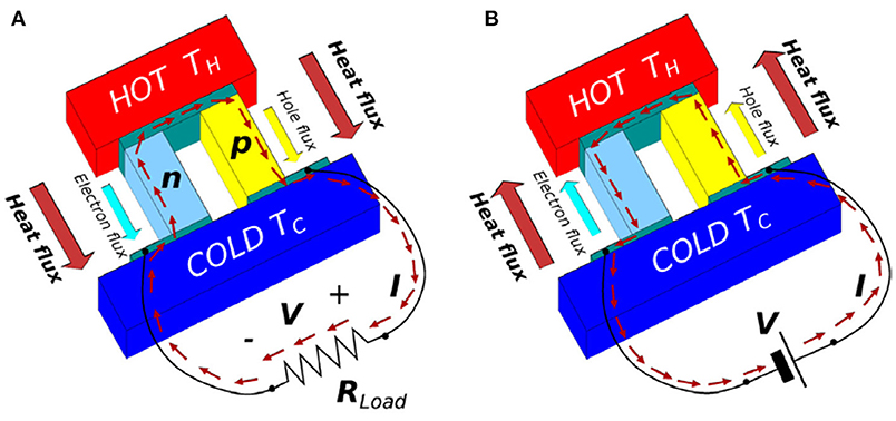
Figure 1. Sketch of thermoelectric device: (A) Thermoelectric generator; (B) Thermoelectric cooler. Reprint with permission from Pennelli (2014). Copyright 2014 Journal of Nanotechnology.
ZT and Energy Conversion Efficiency
To measure the TE energy conversion efficiency of TEG, researchers adopted the parameter called dimensionless figure of merit, denoted as ZT, which is defined as (Rowe, 1995):
where S is the Seebeck coefficient, σ the electrical conductivity, T the operating temperature, and κ the thermal conductivity. In some cases, when κ is unavailable for ZT calculation, the parameter which is defined as TE power factor:
can be an indicator (Rowe, 1995). To improve the TE property of TEG, two approaches have been considered: (1) improve the power factor S2σ, (2) decrease the thermal conductivity κ. Since electron scattering in a semiconductor is negligible, interest has been focusing on the method to lower the thermal conductivity.
For the conventional TEG, ZT is defined as (Rowe, 1995):
where the subscripts p and n denote the P-type and N-type legs, respectively.
The maximum conversion efficiency is defined by (Rowe, 1995):
where η0 = (Th – Tc)/Th is the Carnot ideal cycle efficiency. Here, the Th is the hot junction temperature, Tc for the cold side. ZTavg is the average value of ZT from Tc to Th. The certain relations between Th, ZTavg, and η are shown in Figure 2 (Yu et al., 2019). Like other types of heat power generation, η increases with temperature difference and is confined to the Carnot limit (Gadea et al., 2018a). Conversion efficiency of different types of energy sources for electric generations like geothermal, solar, nuclear, and coal are also presented in Figure 2, which can be a comparation.
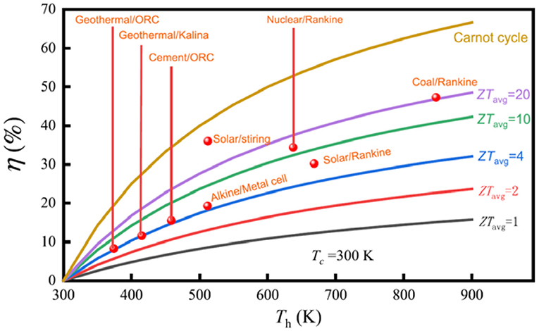
Figure 2. TE energy conversion efficiency (η) vs. hot-side temperature (Th) for different ZTavg values. Reprint with permission from Yu et al. (2019).
The highest ZT has achieved more than 2 for some materials (Kumar et al., 2020), and there are some calculations and models which speculated that there is still potential for ZT. But it is noteworthy that for different temperatures, the ZT varies widely; the most valuable temperature is 300 K, which is the device's normal operate temperature. For Si, ZT = 0.2 is achieved at 620 K with the optimized contact in a recent work (Gadea Díez et al., 2020).
Thermal Conductivity
Fourier's law is defined as: j = –κ∇T, where thermal conductivity κ is the ratio of heat flux j that passes through unit area per unit time to temperature gradient ∇T (Swinkels and Zardo, 2018). In a semiconductor, κ = κph + κe is the sum of two main parts, dominating phonon thermal conductivity and negligible electron thermal conductivity κe. Phonon thermal conductivity κph = LphvsCv/3 is related to heating transport through phonons, depending on the phonon's mean free path of certain materials (MFP, Lph = vsτ is the phonon mean free path, with τ phonon lifetime), sound velocity (vs), and heat capacity (Cv). Electron thermal conductivity is calculated by the Wiedemann-Franz law κe = L0σT where L0 ≈ 2.45 × 10⁻⁸ V2 K−2 is theLorentz constant for degenerately doped silicon (Minnich et al., 2009), representing heat propagation with charged carriers, σ the electrical conductivity, and T the average temperature between the cold and hot side. Molecular dynamics (MD) and first principle calculation techniques have been used in several studies to calculate the theoretical value of the thermal conductivity of Si and SiGe (Chen et al., 2009; Garg et al., 2011; Yang and Minnich, 2017).
Phonon Thermal Conductivity
Thermal conductivity is actually related to the lattice thermal conductivity, and it consists of different kinds of phonon scattering. This is caused by defects or dopants with disorganized lattice periodicity; the scatterings reduce the MFP to a large extent. Other particles and quasiparticles, like electrons, can also produce scattering using the energy and momentum exchange. These scattering mechanisms have been formulated by the Matthiessen's rule (Gadea et al., 2018a):
In the above formula, the phonon relaxation time is comprised of multiple phonons scattering events including phonon–phonon normal scattering, phonon–phonon Umklapp scattering, phonon alloy scattering, phonon boundary scattering, phonon cluster scattering, and phonon electron scattering (Yi and Yu, 2015).
Mainly, researchers focused on the most important parts like phonon-boundary scattering and phonon alloy scattering. Although phonon boundary scattering is frequency independent, it is mainly influenced by the low frequency phonons with long wavelength (Kim, 2013). Phonon boundary scattering is caused by the grain boundary and it is dominant where the dimension of the structure is much smaller than the phonon MFP. Therefore, the phonon thermal conductivity is strongly depressed and the heat flux through the system is limited by the thermal boundary Kapitza resistance (Cahill et al., 2003). For silicon NW, its phonon mean free path is ~300 nm while its electron mean free path is ~110 nm with heavy doping (Ju and Goodson, 1999). Considering this, the diameter of a Si NW should be thinner than 300 nm but more than 110 nm. Then the κ will be reduced for that κph = LphvsCv/3, so the thermal conductivity of a single Si NW decreases when the diameter decreases.
When we discuss the influence of phonon boundary scattering on the κ, the surface roughness of the NWs is an important issue. Thermal conductivity reduction caused by surface roughness has been observed in several experimental works (Hochbaum et al., 2008; Kim et al., 2011; Feser et al., 2012; Malhotra and Maldovan, 2016); κ was reported with a value down to few W m−1 K−1 in NWs with a diameter of several tens of nms, much lower than the bulk Si (~150 W m−1 K−1). By theoretical prediction, the κ in Si NWs with a diameter <100 nm was proportional to (D/Δ)2, where D was diameter and Δ the surface roughness. An analysis shows that the experimental data fits well with the calculation data, indicating the dependence between D and κ (Figure 3).
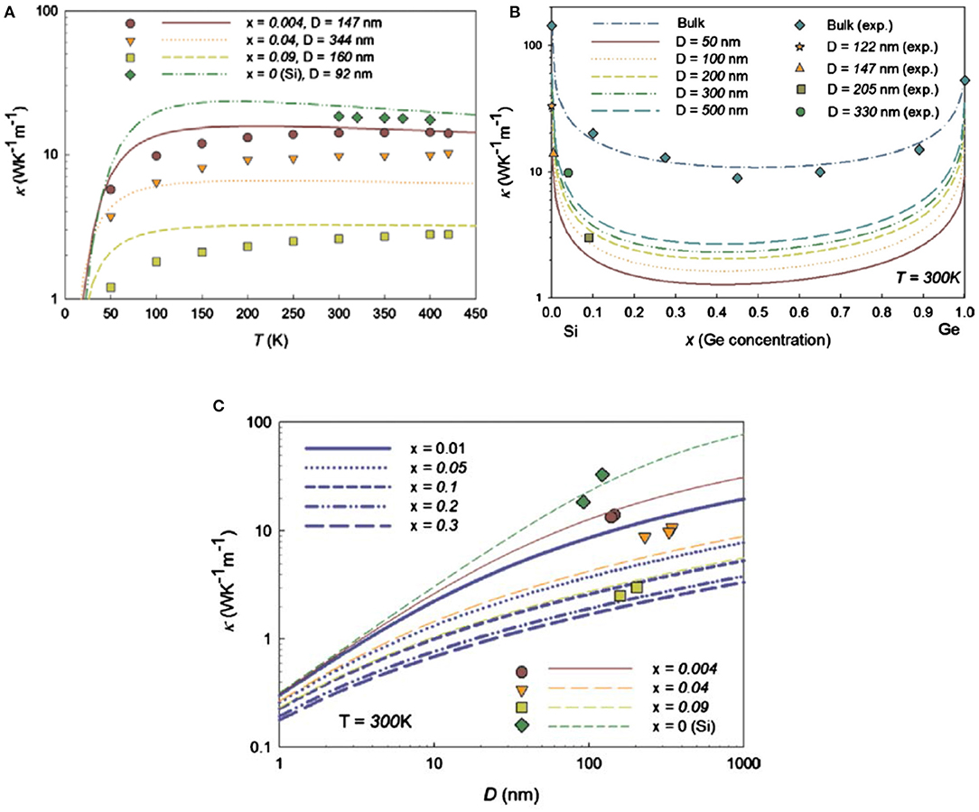
Figure 3. Calculated and measured thermal conductivity of Si1−xGex NWs for different (A) temperatures, (B) Ge concents (at room temperature), and (C) diameter. The symbols are experient data from Kim et al. (2010) and Steele and Rosi (1958). Reprint from Wang and Mingo (2010).
Other mechanisms, like point defect scattering in Si1−xGex alloy, also result in the reduction of λph. Figure 3 shows the κ behavior of Si1−xGex NWs with Ge concentration x = 0.004, 0.04, and 0.09. The figure reveals that the alloy scattering is aggravated by the increased Ge content. At the same Ge concentration, the thermal conductivity is decreased with a smaller diameter, which has been confirmed in previous research (Li et al., 2003b). In principle, alloy scattering causes a severe suppression of high-frequency phonons in Si1−xGex, thus the low frequency phonons became the dominant ones (Xie et al., 2014). Meanwhile, compared with Si NWs, a stronger length dependence, weaker diameter, and surface roughness dependence have been shown to occur in Si1−xGex NWs thermal conductivity (Xie et al., 2014).
Electron Thermal Conductivity
Besides the reduction of phonon thermal conductivity, there is also an alternative approach which is based on tailoring the electronic transport properties. Electron thermal conductivity κe = L0σT depends on the density and mobility of the carriers in L0, and it is strictly related to the electrical conductivity σ. Electronic thermal conductivity is high in metal materials but much lower in semiconductors due to their different thermal conduction mechanism. It is noteworthy that once the κph is largely suppressed by effective phonon scatterings in bulk nanostructure, κe become dominant and the ZT can be simplified to ZT = S2σ/T, making it totally electronic.
Using the electron energy filtering effect, the thermal conduction from the carrier density is reduced, and thus κe is largely reduced. Meanwhile, the filtering causes a decrease of the Lorenz number, which further reduces the κe and makes the κph dominant one (Bahk et al., 2013). The energy filtering effect has been researched in the bulk nanostructured Si, SiGe, and PbTe (Martin et al., 2009; Minnich et al., 2009; Narducci et al., 2015), and it has also been demonstrated in the Si NW (Bennett et al., 2015). The energy filtering is also important for PF, which we will discuss in the next section.
Power Factor
In addition to reducing thermal conductivity, the enhancement of power factor is another approach for the TE performance improvement. PF = σS2 is related to the electronic transport, and it is better to simultaneously improve both the electrical conductivity and the Seebeck coefficient for the optimal PF (Mehdizadeh Dehkordi et al., 2015). For the optimal TE performance, the ideal doping concentration is between 1019 and 1021 cm−3, which depends on the electronic band structure of materials (Tritt, 2011; Schierning, 2014). The relations between the TE parameters and doping concentration for the alloy Si80Ge20 are shown in Figure 4; κ, σ, S, and ZT vary with the doping concentration in different tendency (Minnich et al., 2009).
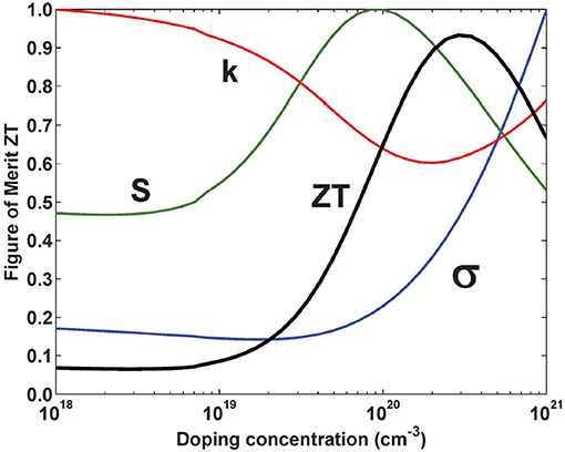
Figure 4. Normalized TE properies and ZT vs. doping concentration at 300 K for N-type Si80Ge20 (Minnich et al., 2009).
A simulation has studied the optimal power factor in Si NW with different sizes, and the relation of S, σ, and PF vs. the cross-section area (area) and carrier concentration (n) are shown in Figure 5 (Shi et al., 2009). The thinner Si NW will have larger S and smaller σ, and thus slightly increase the PF, and proper carrier concentration is needed for the optimal PF.
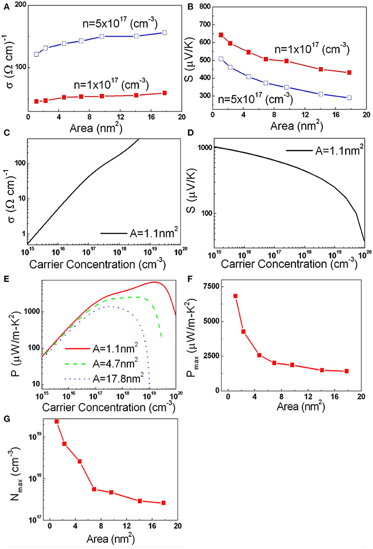
Figure 5. (A–D) S, σ vs. area, n; (E–G) PF (P), optimal PF (Pmax), optimal carrier concentration (Nmax) vs. area, n. Reprint from Shi et al. (2009).
The research studies about the TE power factor enhancement are based on the nanostructures of different materials to a great extent (Mehdizadeh Dehkordi et al., 2015); here we only give a brief introduction of the mechanism of electrical conductivity and Seebeck coefficient.
Electrical Conductivity
The electrical conductivity is always an important parameter for electronic devices as well as for TE ones. This parameter is mainly dependent on Kelvin temperature and the electronic relaxation time in a material. In principle, the carriers can interact with different scattering centers e.g., impurities or phonons, and the relaxation time may be affected. More specifically, the scattering centers are categorized by ionized and neutral impurities (I and N) and deformation potential (D) created by phonons. These scatterings mostly occur simultaneously, therefore, the total relaxation time is written by Matthiessen's rule (Yi and Yu, 2015).
The deformation potential is governed by electronic carriers scattering through the acoustic vibration of atoms in the crystal lattice and intervalley scattering caused by optical phonons (Yi and Yu, 2015). The modulation-doping is remarkable for the ionized impurity scattering which is dominant at a low temperature (Mehdizadeh Dehkordi et al., 2015).
Seebeck Coefficient
Based on the Seebeck effect (Figure 1A) found in 1821, Seebeck voltage V is proportional to the temperature difference ΔT and Seebeck coefficient S (also thermopower) (Gadea et al., 2018a):
The Seebeck coefficient for semiconductors is typically on the order of 100 μV/K (Goktas et al., 2018). Conversely, this process can operate in reverse to make TE cooler (the Peltier effect, Figure 1B). In P-type semiconductors, S is a positive value (negative in N-type semiconductor). In the fabrication of a TEG, both N-type and P-type are applied to achieve a larger potential difference.
For metals and degenerate semiconductors, the Seebeck coefficient is defined as (Snyder and Toberer, 2008),
where n is the charge carrier concentration, m* is the effective mass of the charge carrier, h is the Planck's constant, kB is the Boltzmann constant, and e is the carrier charge. S is strongly influenced by the charge carrier energy distribution, and in particular it increases when the average difference between the carrier energies and the Fermi energy increases (Pennelli, 2014).
Dopants, defects, and interfaces can act as energy barriers. The caused energy filtering effect will suppress the low energy electrons in the transport, and thus increase the S and PF in a semiconductor (Schierning, 2014). Hicks and Dresselhaus (1993a) have presented a study about the effect of electron quantum confinement on TE properties of NWs. The results show that interfaces cause energy barriers as energy filtering for low energy electrons which are not active in the transport, resulting in an enhancement of PF (Martin et al., 2009). The enhancement of PF in combination with the reduction of the κ are the two benefits for quantum dot and quantum well structures where density of electronic states is modified and phonon modes are frozen. The TE properties of quantum dots and quantum wells are both theoretically foreseen (Hicks and Dresselhaus, 1993b) and experimentally demonstrated (Harman et al., 2002).
The longer SiGe NW arrays provide higher S and then κ is decreased by increasing Ge content and NW length (Li et al., 2012). A TEG with short planar Si NWs have demonstrated a dramatic enhancement in the TE power density, attributing to the increase in S (Tomita et al., 2018a). This was explained by the enhanced phonon drag effect, since the frequent surface scattering in longer Si NWs will weaken this effect (Figure 6).
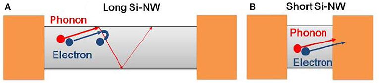
Figure 6. Schematic of the thermal carrier behavior in the (A) long Si-NWs and (B) short Si-NWs. Reprint with permission from Tomita et al. (2018a).
Advanced Group IV Materials
Since the electric conductivity of a TEG was decreased as a result of pursuing the high thermal conductivity, the better choice is an ideal material which integrates the opposite properties of low thermal conductivity and high electric conductivity (σ), with an as high as possible Seebeck coefficient (S). Therefore, the concept called phonon glass-electron crystal (PGEC) has been put forward which involves limiting the minimum electron scattering (small electron mean free path), like the crystalline material, and high phonons scattering (large phonon mean free path), like the amorphous material.
Bismuth telluride (Bi2Te3) and its (Bi1−xSbx)2(Se1−yTey)3 alloy family are the most used TE materials because of their high TE conversion efficiency at room temperature. Also, their easy deposition in thin film makes the module flexible (Siddique et al., 2017). However, the process price of these traditional foundation materials is also an important issue. A review of the material price of the TE is listed as: Lead (Pb ~2.50$/kg), Bismuth (Bi ~10.5$/kg), Antimony (Sb ~9$/kg), Selenium (Se ~24$/kg), or Tellurium (Te ~36$/kg) (Haras and Skotnicki, 2018). As a comparison, the pristine silicon is much cheaper as a TE material due to the increase in photovoltaic power generation (Si ~1.5$/kg). Silicon also has the advantage of being low cost with the CMOS-compatible processing. Furthermore, when counting other recessive and dominant costs, like environment friendliness and human innocuous, there is no doubt that silicon has an overwhelming preponderance.
Si NWs
With the diamond structure (Fd-3m), silicon conducts heat largely by phonon rather than the charge carrier (electron or hole). At 300 K, thermal conductivity of pure silicon is ~150 W m−1 K−1 (Glassbrenner and Slack, 1964). With doping, the thermal conductivity can be further reduced due to phonon impurity scattering (Slack, 1964). Silicon NW has shown its priority in TE application. Compared with bulk Si, an extreme reduction of thermal conductivity (1.6 W m−1 K−1) has been demonstrated for Si NWs with a 50 nm diameter without the detriment of Seebeck coefficient and electrical resistivity values (Hochbaum et al., 2008). The strong diameter dependence of Si NWs thermal conductivity has been demonstrated, which is attributed to the enhanced phonon-boundary scattering and phonon spectrum modulation (Li et al., 2003b). The similar reduction of thermal conductivity from bulk to NWs has also been reported in Ge-based TE research. A sub-30 nm diameter Ge NWs was measured with a thermal conductivity of ~1.5–2.3 W m−1 K−1 at 300 K (Wingert et al., 2011), dramatically decreased from Ge bulk (~56 W m−1 K−1) (Glassbrenner and Slack, 1964). Also, we can see a decrease of thermal conductivity compared to the Si NWs mentioned above, and the difference is explained by the heavier atomic mass and decreased phonon velocities of Ge with respect to Si (Wingert et al., 2011).
Si NW arrays, which are largely parallel Si NWs, have been fabricated on Si substrate with metal-assisted chemical etching (MaCE) in order to make a TEG. With an amount larger than 107 in several mm2, a 0.5 mm thick sample chip, and NWs diameter between 60 and 120 nm, the thermal conductivity was measured at ~ 4.6 W m−1 K−1 (Pennelli et al., 2018).
Isotope doping can be a feasible way to reduce thermal conductivity. Isotope effect on the thermal conductivity of Si NWs has been researched theoretically based on the non-equilibrium molecular dynamics (NEMD) method (Yang et al., 2008). Random isotope doping Si NWs and isotopic-superlattice Si NWs are built in this research, the minimum thermal conductivity is 0.4 W m−1 K−1 is shown in 28SiSi0.5 NWs with cross sections of 1.6 × 1.6 nm2. Furthermore, a curve of thermal conductivity vs. the concentration of doping isotope atom (x) is exhibited, which shows a similar tendency with SixGe1−x and a plateau at 0.2 <x<0.8 (We will discuss this tendency in the next section). More simulations have been conducted for the isotope effect on thermal conductivity, like the isotopic core-shell Si NWs (Hattori and Uno, 2013) and isotope radial distribution (Royo and Rurali, 2016). The fabrication of Si isotope NWs is demonstrated in Mukherjee et al. (2015) using the VLS method and a 30% decrease of thermal conductivity is shown in isotopically mixed 28SiSi1−x NWs compared with isotopically pure 29Si. This is in agreement with the aforementioned simulation.
Si1−xGex Alloy NWs
Starting in the 1970s, SiGe alloys have been applied in RTGs for the power systems in NASA space missions (with ZT ~0.5 for P-type and ~0.9 for N-type at 1,073 K; Rowe, 1995). Later improvements were realized in nanostructured bulk SiGe with ZT ~1.3 at 1,173 K for N-type (Wang et al., 2008a) and ZT ~0.95 at 1,073 K for P-type (Joshi et al., 2008). A recent study has fabricated Si80Ge20B0.5 bulk alloy with the maximum ZT of 0.71 at 1,073 K using melt spinning (MS) combined with spark plasma sintering (SPS) (Wongprakarn et al., 2018).
Like Si NWs, SiGe alloy NWs exhibited excellent enhancement as a result of the phonon boundary scattering. Individual P-type SiGe alloy NW was reported with thermal conductivity ~1.1 W m−1 K−1 and ZT ~0.18 at 300 K experimentally (Martinez et al., 2011). In a typical TE modeling of SiGe NWs, the optimized ZT is 1.3 at 800 K for the Si0.73Ge0.27 NW with 26 nm diameter where the ionized impurity concentration should be about 1.0 × 1020 cm−3 (Yi and Yu, 2015). In principle, the ZT of SiGe at different temperatures can be further enhanced by the diameter reduction and doping concentration optimization. The reduction in SiGe alloy NWs came from the phonon alloy scattering which scatters short wavelength phonons with high frequency, while low frequency phonons are scattered by the phonon boundary scattering (Li et al., 2003a).
Several studies have investigated the effect of Ge fraction (x) on the thermal conductivity (κ) in Si1−xGex NWs both theoretically and experimentally (Wang and Mingo, 2010; Li et al., 2012; Yi and Yu, 2015). In an MD simulation, with x = 0.05, the κ of SiGe NW was decreased to half of that of the intrinsic Si NW, and the minimum thermal conductivity was shown at x = 0.5, which is reduced to only 18% (Chen et al., 2009). With a similar tendency found in bulk SiGe alloy, it has been shown that a dramatic reduction of thermal conductivity happens when the Ge concentration increases in a small scale less than x = 0.005 (Wang and Mingo, 2010). The further increasing of Ge content will decrease the thermal conductivity to approach the lower limit which is achieved at x ≈ 0.4. In fact, with x = 0.2, the thermal conductivity has approached the minimum and then a broad plateau exists in the range of 0.2 <x<0.8 (Figure 3B). Such a plateau is caused by the phonon alloy scattering due to the large atomic mass difference between Si and Ge (Khatami and Aksamija, 2016). Then, the excessive Ge content makes the thermal conductivity dramatically reversing increase, and the κmin of NWs is much smaller than the bulk one.
A study on the surface doping effect shows different types of alloying of SiGe, and Ge are used in a small fraction as a dopant on the surface of Si NWs with a facile fabrication (Pan et al., 2015). Compared to pristine Si NW, the Ge-coated Si vertical NW arrays show a 23% reduction in thermal conductivity at 300 K, and such a decrease can be enhanced to 44% by annealing. Analyzed by X-ray photoelectron spectroscopy (XPS), the interaction between Ge surface doping and Si NWs is enhanced by the binding energy shifting of Si-2p and Ge-3d after annealing treatment. Moreover, simulated results by MD method shows the SiGe composition has to be graded in order to effectively optimize the thermal conductivity. Compared to the SiGe with abrupt interfaces, a 57% reduction of thermal conductivity was reported for the graded SiGe NW (Zhang et al., 2017).
Besides Ge fraction, diameter (D), and length of SiGe NWs are also important issues for the TE properties (Li et al., 2003b; Wang and Mingo, 2010). The thin NWs show a reduction of thermal conductivity when compared with the thick ones. A thorough study has been designed to find the certain trend (Shi et al., 2009), and the result is that thermal conductivity is proportional to D when D is small. However, this dependence becomes continually weaker with increasing D. Combined with the Ge constituent effect, the group found the linear trend slowed down with a higher Ge content, up to x = 0.5. The same situation happens with the increasing Si in Ge. This is because of the coexistence of alloy and boundary scattering. SiGe NW arrays with a longer length exhibit a higher Seebeck coefficient while the thermal conductivity decreases with increasing Ge concentration and NW length (Li et al., 2012).
When it comes to doping type, N-type SiGe NWs are reported to have remarkably higher ZT and power factor compared to P-type SiGe NWs at 300 K (Shi et al., 2010). With a cross section area of 2.3 nm2, the ZT of N-type Si1−xGex NWs was theoretically calculated to be ~4.3 (Shi et al., 2010). In Noroozi et al. (2017a), the peak of Seebeck coefficient for N-type and P-type Si0.53Ge0.47 are 8 and 1.8 mV/K at 315 K, which can be explained by the temperature dependence of the interaction of defects. With the same diffusion process applied, the carrier mobility in N-type SiGe NWs is higher than P-type, which results in a much higher Seebeck coefficient in N-type SiGe NWs than P-type. Also, the measured maximum power factor of N-type is two times higher than P-type.
Other Promising Group IV Materials
With the prosperity of silicon-based technology, other Group IV materials have also been studied as composite materials. They have similar crystal textures, so they have lower processing costs and high compatibility. With the publications of theoretical and experimental research, it was discovered that carbides and tin compounds with silicon and germanium have excellent TE properties.
SiC
As the recognized third generation semiconductor material, SiC has become a promising material for power electronics. Different advanced growth methods have been applied to improve the crystal quality (Pécz et al., 1999; Yakimova et al., 2011). SiC has also been applied to other semiconductor devices including composites, field emitters, supercapacitors, field-effect transistors, nanoelectromechanical devices, photocatalysts, sensors, microwave absorbers, and super-hydrophobic coating (Zekentes and Rogdakis, 2011; Wu et al., 2015; Chen et al., 2019). A lot of studies have presented the performances of SiC. Under those investigations, SiC exhibits excellent mechanical properties, exceptional chemical stability, high power, high frequency, thermal stability, and low thermal conductivity (Zekentes and Rogdakis, 2011; Wu et al., 2015; Chen et al., 2019). Some people have investigated its TE properties to seek for the possibility of SiC as a TE material (Choi et al., 2011). The revealed characteristics demonstrated the possibility for SiC as a superb TEG material which can work in harsh ambiences like high-power/high-temperature/high-voltage.
Both theoretical and experimental studies have been carried out for the thermal properties of SiC NWs. NEMD simulations were used on the lattice thermal conductivity of bulk β-SiC and NWs (Papanikolaou, 2008). Like Si and SiGe, a dramatically reduced thermal conductivity has been shown in SiC NWs compared to the bulk SiC, similarly owing to the boundary scattering and size confinement of phonons in nanostructures. In another piece of research based on NEMD, the thermal conductivity of SiC NWs with modulated diameters and polytypes were predicted, and it was also found that the increase of both the diameter and length can enhance the thermal conductivity of SiC NWs with the similar tendency of Si NWs (Termentzidis et al., 2013). A repeatable method involved placing the individual or double β-SiC NWs on pre-patterned electrodes via a nanomanipulator combined with focused ion beam (Lee et al., 2010), and the 3ω method measured thermal conductivities of the individual and double NWs were, respectively, 82 ± 6 and 73 ± 5 W m−1 K−1. Likewise, the thermal conductivity, electrical conductivity, and Seebeck coefficient of SiC NWs were reported as a function of temperature for the SiC NWs from 190 to 370 K (Valentín et al., 2013). The Seebeck coefficient was measured varying from −17 to −68 μV/K with the temperature range, and at 300 K the S varied from −22 to −56 μV/K, for N-type doped SiC (Valentín et al., 2013). A simulation study demonstrates that the thermal conductivity ranged from 4 to 12 W m−1 K−1, near 5 W m−1 K−1 for ~ 4 nm diameter. Similarly, the reduced diameter also decreased the thermal conductivity of SiC NWs by comparing the three samples with different sizes. However, compared with the electric property searching of SiC for microelectronic devices, the experiments for the TEG are still insufficient, thus more research should be carried out in this field.
Si-Ge-Sn Binary and Ternary Alloys
Compared to C, Si, and Ge, Sn has a larger atomic mass and bigger atom diameter. The size difference has a large impact on TE performance. A variety of studies have demonstrated their alloy effects significantly decrease thermal conductivity.
Theoretically, a group investigated the Sn alloying effect to SiGe on the thermal conductivity (κ) of SiGeSn alloys using NEMD simulations with optimized Stillinger–Weber parameters (Lee and Hwang, 2017). The afore-mentioned broad plateau in SiGe alloy also appeared in the ternary alloys. With a realizable content range in 0 ≤ x ≤ 0.2, the κ of Si0.2−xGe0.8Snx alloy was much lower than the SiGe and GeSn alloys. The predicted minimum of κ occurred at x = 0.1 with a ~40% reduction compared to those of Si0.2Ge0.8 and Ge0.8Sn0.2. This reduction is produced by the increased mass disorder scattering of phonons similar to SiGe. Another theoretical study with phonon Boltzmann transport formalisms have simulated the phonon thermal conductivity of SiSn, GeSn, and SiGe-Sn alloys and their corresponding thin films (Khatami and Aksamija, 2016). They showed that the minimum thermal conductivity of Si1−xSnx alloys was 3 W m−1 K−1 with x = 0.5 and 5.86 W m−1 K−1 for the Ge1−ySny with y = 0.61, which can be the lowest of the three alloys, twice as low as SiGe. In contrast, their simulation of the 20 nm SiGe, SiSn, and GeSn thin films offer a further decrease in κ with a value of 1.71 W m−1 K−1 for the Si0.51Ge0.49, 0.91 W m−1 K−1 for the Si0.41Sn0.59, 1.53 W m−1 K−1 for the Ge0.45Sn0.55, and 1.11 W m−1 K−1 for Si0.36Ge0.32Sn0.32 which are near the conductivity of amorphous SiO2 (Khatami and Aksamija, 2016). Both pieces of research theoretically show the TE potential of Sn incorporated with SiGe.
Experimentally, phosphorous-doped Ge0.971Sn0.029 NWs is fabricated using RPCVD and its electrical conductivity and Seebeck coefficient data is compared to the Si and Ge NWs at 250 K for NWs with cross-sectional area of 700 × 50 nm and length 22 μm. The GeSn is measured with electrical conductivity ~550 Ω−1 cm−1, which is much larger than Si (231 Ω−1 cm−1) but less than Ge (653 Ω−1 cm−1), and Seebeck coefficient ~67 μV/K, larger than Si (42 μV/K) or Ge (47 μV/K). The calculated power factor is 0.24 mW m−1 K−2, superior to Si (0.041 mW m−1 K−2) and Ge (0.14 mW m−1 K−2) (Noroozi et al., 2014). The electronic properties of Ge0.81Sn0.19 NWs were studied in the temperature range of 10–298 K, and resistivity of Ge0.81Sn0.19 NW (~1 × 10⁻⁴ Ω m) was 100 times lower than the pure Ge (~9 × 10⁻³ Ω m) at room temperature (Sistani et al., 2018). The difficulty for the high Sn content in SiSn alloy fabrication (and, to a lesser extent, Ge-Sn) comes from the 19.5% lattice mismatch between Si and α-Sn, and Sn has a low solid solubility (~5 × 1019 cm−3) in Si (Min and Atwater, 1998). No experimental data of SixSn1−x and GexSn1−x NWs have been found for the thermal conductivity yet, which may be a sally port for TE material research.
Advanced Structures
The effective TE performance modulation by diameter and alloying have been proven theoretically and experimentally. New atomic-scale designs and surface structure as toolkits for thermal conductivity control are also under investigation (Özden et al., 2015). To reduce the time and cost of the experiments, several calculation models have been proposed to simulate new nanostructures. These structures affect the TE performance by modulating various scattering events we mentioned in Chapter 2 such as phonon normal scattering, phonon boundary scattering, and phonon Umklapp scattering.
Many possible structures have been considered on the foundation of SiGe alloy NW μTEGs with high TE performance in the past decades, like core-shell (C-S) (Hu et al., 2011; Markussen, 2012), superlattice (SL) (Lee et al., 1997; Huxtable et al., 2002; Li et al., 2003a), etc. Compared with the pure NWs, these structures further suppress the thermal conductivity by enhancing various phonon scattering owing to the lattice mismatch of ~4% between Si and Ge.
In a recent theoretical work, pristine, core-shell, holey, superlattice, sawtooth, and superlattice sawtooth Si/SiGe NWs with identical structural parameters were investigated (Özden et al., 2015). A comprehensive comparison of thermal conductivity in those different nanostructures was performed by using equilibrium molecular dynamics (EMD) simulations with Green-Kubo method at room temperature. The results demonstrated that thermal conductivity can be minimized by varying the specific parameters e.g., the core diameter and monolayer separation for Core-Shell (C-S), holey, and sawtooth structures. However, for SL structures, the thermal conductivity is independent of the above-mentioned parameters. The lowest thermal conductivity in these structures has been demonstrated for the sawtooth superlattice NW, with κ <2 W m−1 K−1 (Özden et al., 2015).
Core-Shell (C-S)
The SiGe C-S structure is a radial heterostructure of Si and Ge. SiGe alloys have been used in many electronic devices, such as stressor and high mobility channel materials, for years. Both Ge or SiGe layers could be grown selectively in trenches or around SiNWs as core layer (Grahn et al., 2000; Hållstedt et al., 2008b; Radamson and Kolahdouz, 2015). The interface between core and shell reduces thermal conductivity by phonon scattering. A successful synthesis of Ge-Si core-shell NWs with no branch has been reported recently and the synthesis processes were elaborated in detail (Noguchi et al., 2016).
Wingert et al. has synthesized sub-20 nm diameters Ge and Ge-Si C-S NWs by VLS-CVD method (shown in Figure 7; Wingert et al., 2011). Particularly, κ of the C-S NWs at 388 K is 1.1–2.5 W m−1 K−1, remarkably reduced from the Ge NWs (2.3–3.9 W m−1 K−1).
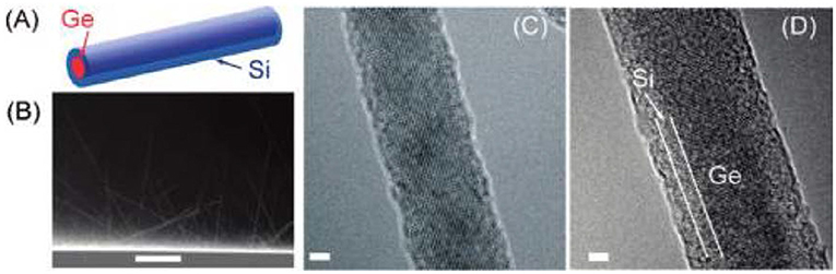
Figure 7. Ge and Ge-Si C-S NWs: (A) Schematic illustration of a Ge-core Si-shell NW. (B) SEM imaging of Ge-Si C-S NWs grown on a Si substrate. (C) High-resolution TEM imaging of a (110)Ge NW. (D) HRTEM imaging of a Ge-Si C-S structure by epitaxially growing the Si shell on the (110)Ge NW. Reprint with permission from Wingert et al. (2011). Copyright 2011 American Chemical Society.
Some theoretical works have applied first-principle calculations and Boltzmann transport theory to model the TE performance of Ge/Si or Si/Ge core-shell NWs (Wingert et al., 2011; Yang et al., 2015; David et al., 2017). In a study (Chen et al., 2010), with the optimal carrier concentration of 2.64 × 1025 m−3, the achieved maximum ZT value reached 0.85 at 300 K in Ge/Si C-S NWs with P-type doping, significantly larger than 0.36 in pure Si NWs. Moreover, they verified the chances for the further improvement of the C-S NWs by optimized core/shell radius ratio, NW sizes, doping, orientation, and surface structure (Chen et al., 2010). Several factors, such as the core/shell radius ratio, may influence the C-S thermal conductivity (Lü, 2009): (1) The C-S structures have a weaker length dependence compared to pristine NWs due to the diffusion dominant phonon transport, and the thermal conductivity of C-S is even low for the long NWs; (2) The thermal conductivity of C-S structure is practically independent of the temperature in the range of 50–600 K, which shows a confinement of the core by the shell; and (3) Unlike the monotonic impact on the thermal conductivity of pure NWs, the increasing diameter of the core-shell NWs first reduced the thermal conductivity to a minimum then boosted it because of the contrast from core center vs. shell surface.
Superlattice (SL)
Semiconductor SLs are attractive for their potential as TE materials (Li et al., 2003a). The traditional 2D SL is the multilayer thin films of different materials that are alternately periodically stacked, and 1D NW SL is the axial heterostructure NW of different materials which can be seen as a series of interlaced nanodots of these different materials (Chen et al., 2011). Due to the periodic modulation of energy gaps by the adjacent nanodots, the TE properties can be improved. The different scattering mechanisms are demonstrated in Dames and Chen (2004), which can be explained by Figure 8. In SLs, heat transport is modulated by various phonon scattering phenomena (Li et al., 2003a): alloy scattering, interface scattering caused by the mismatch in acoustic impedance, and scattering by lattice mismatch from imperfections. The energy filtering mechanism is also effective in the research of superlattices (Thesberg et al., 2016).
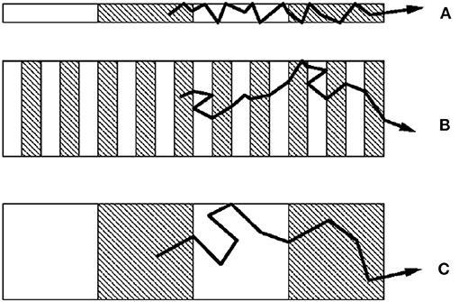
Figure 8. Dominating scattering mechanisms in superlattice NWs (A) diameter limited; (B) superlattice limited; (C) bulk limited. Reprint from Dames and Chen (2004).
Lee et al. (1997) have fabricated 2D Si/Ge SL with SL periods from 30 to 300Å, the thermal conductivity was measured at <5 W m−1 K−1. Monocrystalline Si/SiGe superlattice NWs were synthesized block-by-block based on hybrid pulsed laser ablation/chemical vapor deposition (PLA-CVD) method in 2002 by Wu et al. (2002). Later, the thermal conductivity of Si/SiGe SL NWs with 58 and 83 nm diameter was measured from 20 to 320 K. The value varied from 1 to 7 W m−1 K−1, lower than the SiGe alloy film, 2D Si/SiGe SL film, and intrinsic Si NWs at the same temperature (Li et al., 2003a). Among different research groups, Si/Ge SL NWs with a diameter below 20 nm were reported by using metal-assisted etching (Geyer et al., 2009).
Owing to the difficulty in the SL fabrication, more recent research about superlattice are based on simulations (Xiong et al., 2014; Mu et al., 2015; Hijazi and Kazan, 2016; Qu and Gu, 2020). The MD simulation of Si/Ge SL NWs have reported a 95% reduction by the periodic Si/Ge defects, while amorphization and roughening of the NW surface are utilized (Mu et al., 2015). They concluded that periodicity perturbance can be a useful method for the reduction of SL thermal conductivity by impairing the formation of phonon coherence (Mu et al., 2015).
Other Origin Structures
Sawtooth Si NWs have been fabricated with periodic sawtooth faceting by VLS (Ross et al., 2005). Later, a Monte Carlo simulation demonstrated that the sawtooth roughness caused a thermal conductivity suppression below the limit of diffuse surface by introducing phonon backscattering (Moore et al., 2008). Such surface faceting dependence of thermal conductivity in Si NWs was demonstrated by direct MD simulations and the Si sawtooth NWs with κ ~ 16 W m−1 K−1 was reported (Sansoz, 2011).
Recently, a novel structure, called fishbone NWs, has been synthesized and studied, which is intrinsic silicon NWs with periodic wings (Shown in Figure 9) and the κ of those fishbone NWs were reported between 30 and 50 W m−1 K−1 (Maire et al., 2018). The researchers investigated the heat conduction of this structure through experiments and found that the cross-section of fishbone NWs also controlled the κ, as in pristine NWs, and further reduction was caused by the periodic wings. The increasing wing depth exhibited a significant decrease of κ (this decrease was intensified in narrower NWs) while the wing width only had a slight influence, and these effects were explained by modeling.
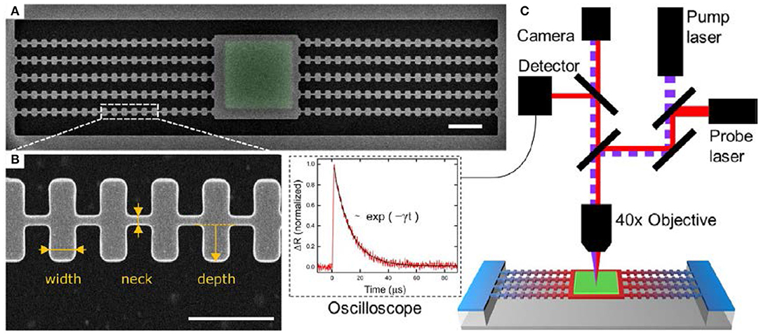
Figure 9. Fishbone NW. (A) SEM image of the suspended fishbone nanostructure; (B) Enlarged top view; (C) Schematic of micro time domain thermoreflectance setup, with recorded signal and exponential fit. Reprint with permission from Maire et al. (2018).
There is a study on the TE properties about a gate-all-around (GAA) structure Si NWs (Curtin and Bowers, 2014). Using multi-subband Boltzmann transport formulation and relaxation time approximation, a GAA Si NW with a cross-sectional area between 4 × 4 nm and 12 × 12 nm was simulated and compared with experiment. With the charge carriers induced with the electrical gate, no ionized impurity scattering was discovered; meanwhile, the mobility and electrical conductivity were increased compared to the doped materials. The smaller cross-section of the Si NWs showed stronger quantum confinement, which means an improvement of the Seebeck coefficient. This also exhibited an enhanced electrical conductivity in a smaller cross-section. The maximum power factor of the 6 × 6 nm Si NWs achieved 6.8 × 10⁻³ W m−1 K−2 (Curtin and Bowers, 2014).
Though many Si/Ge/SiGe-based novel structures have been simulated to study the TE properties, few have been achieved in the experiments. Even fabricated, they are not applied in the TE field. Further experiments are indispensable for those structures to be used in TE devices.
Material Growth and Fabrication of μTEG
Si NWs can be fabricated only in the <100>, <111>, <110>, or <112> directions depending on their diameter and the substrate (Wang et al., 2008b). For industrial manufacturing, the (100) Si wafer are the most common substrates, and the vertical Si <100> NWs can be easily utilized by the etching process (Wolfsteller et al., 2010). Meanwhile, the <100> crystal orientation also exhibits better TE performance than the <111> in SiGe bulks and NWs (Kandemir et al., 2017). Besides the conventional Si substrate, the most used substrate for Si and SiGe NWs is the <100> SOI wafer for its fabrication convenience and good electrical properties (Barraud et al., 2019). A research group prepared a SiGeOI wafer for the fabrication of SiGe NWs (Noroozi et al., 2017b). The SiGe nanowires operated as an FET transistor with back-gate configuration.
In order to achieve the NWs structure, several fabrication technologies have been proposed and applied. They are classified into two methods: “Bottom-up” and “Top-down.” Bottom-up fabrication is a somewhat easier way to achieve NW growth compared to the Top-down, and it also has the advantages of low cost and massive fabrication. However, more complex processes are necessary for the contacts and connection with NWs. Meanwhile, the top-down method, though expensive, is CMOS-MEMS compatible and allow the fabrication of NWs together with contacts, connections, and control gates. In practical process, the vertical NWs can be easily synthesized by the bottom-up methods for material research, while NWs with both vertical and horizontal orientation are suitable to be fabricated and integrated into the device like TEG with top-down approaches (Ray et al., 2017). Wolfsteller et al. have fabricated the Si/Ge NW heterostructures in both bottom-up and top-down approaches, and the diameter of the NWs are down to tens of nm; the differences between the two approaches have been compared (Wolfsteller et al., 2010). Another approach to form NWs is Sidewall transfer lithography where a sacrificial layer is deposited oxide and later etched to form residuals on both sides of the oxide. The oxide is removed, and the remaining residuals are used as a mask to form the NWs. In this way, very narrow NWs with widths of 20 nm can be synthesized (Hållstedt et al., 2008a).
Bottom-Up
One of the most popular methods for the fabrication of Si NWs in bottom-up approaches is the vapor–liquid–solid (VLS) mechanism (Wagner and Ellis, 1964). With an Au droplet as catalyst, several approaches have been applied to the bottom-up growth of Si, Ge, and SiGe NWs based on the VLS mechanism like chemical vapor deposition (CVD), molecular beam epitaxy, and laser ablation (Ray et al., 2017). The typical process of VLS is illustrated in Figure 10, which follows three different steps: (1) source gas like silane (SiH4) or tetrachlorosilane (SiCl4) is decomposed at the vapor–liquid interface under a high temperature, (2) Si atoms diffuse through Au-Si eutectic, and (3) the Si NWs crystallize at the growing liquid-solid interface (Hållstedt et al., 2008a). The diameter is modulated by the droplet diameter while the length is regulated by the growth time (Kim, 2013).
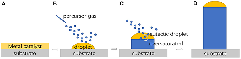
Figure 10. (A–D) VLS growth mechanism. Reprint with permission from Chen R. et al. (2019). Copyright 2019 American Chemical Society.
Based on the VLS methods, a variation named vapor-solid-solid (VSS) was put forward. In this method, the NWs are fabricated at lower temperature than in VLS, which is available for the mass production of devices since it is more compatible with standard industrial processes. There is a report that Si/Ge heterojunction NWs with abrupt interfaces have been grown by VSS (Chou et al., 2012).
The problem for the VLS growth mechanism may lie in the potential inclusion of the metal catalyst during the growth of NWs, because metal catalysts like Au are a detriment for the electrical properties of the Si-based electronics which produce deep-level, carrier recombination centers or cause unintentional doping. Though such problems can be neglected for current Si NWs, it is better to avoid the problem for better device performance. Several analytical technologies, like high-angle annular dark-field scanning transmission electron microscopy (Oh et al., 2008) and secondary ion mass spectroscopy, at the nanoscale are applied for the detection of Au atoms insides Si NWs (Putnam et al., 2008).
Top-Down
The top-down fabrication approach is based on the Si CMOS technology like lithography, etching, and oxidation. The highly anisotropic etching (wet, plasma, and metal assisted) is key to the Si NWs fabrication. Different types of etching are applied in different research, such as silicon alkaline etching, RIE, and MaCE.
Silicon alkaline etching is a cheap and convenient way for etching, and typically uses KOH (potassium hydroxide) or TMAH (tetramethylammonium hydroxide). Based on the anisotropic etching properties of alkaline solution, the etching rate of <111> direction is much slower than other directions like <100>: more than 1/100 between <111> and <100> directions have been shown in a typical 35% KOH aqueous solution at 43°C (Pennelli, 2015).
Using chemical reactive plasma as an etchant, RIE can be applied for the fabrication of Si NWs (Peng et al., 2015). High-energy plasma ions etch the wafer surface and cause surface damage, then the outer atoms are removed from the surface. Suitable materials with high selectivity for the mask are the precondition to fabricate structures on the substrates. The commonly used masks are polymers, SiO2, Si3N4, patterned metal film, or metal nano-particles like Au, Ag, Ni, Al, and W (Ray et al., 2017). Inductively coupled plasma-reactive ion etching (ICP-RIE) has been applied based on RIE while an RF powered electric field is used to generate the plasma, but the ion has a low energy compared to the conventional RIE. Research about the fabrication of CMOS-MEMS μTEG has been reported using RIE; CHF3/O2 is used for the oxide layer while XeF2 is used for the Si substrate (Kao et al., 2010).
MaCE is an electrochemical technique which has been widely used for its low-cost and high yield. Figure 11 has illustrated the procedures of MaCE of silicon NWs under 100 nm and the morphology is imaged by TEM (de Boor et al., 2010). In a typical MaCE procedure (Huang et al., 2011), the Si substrate is partly covered by the metal like Au, Pt, or Au/Pd alloy which acts as catalyst for the etching, then the wafer is immersed to the aqueous solution composed of HF, H2O2, and EtOH. The faster etching rate for the Si beneath the metal causes pores generated in the Si substrate, or in other words, the area without metal can form Si NW. The initial morphology of the metal coverage results in the detailed shape of Si NWs.
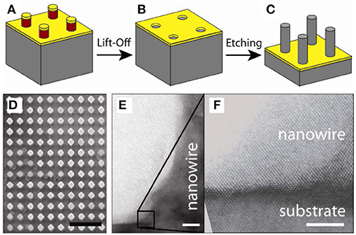
Figure 11. Metal-assisted chemical etching. (A) Metal evaporation, (B) lift-off, and (C) vertical Si NWs array by metal-assisted etchinG, (D) nanowires with diameter about 350 nm, (E) highlighted the root of NWs and the substrate by TEM, and (F) magnified NWs and substrate. Reprint from de Boor et al. (2010) with permission.
Measuring the TE Properties
Principles and Equipment for Measuring
After the fabrication, a series of measurements are necessary to characterize the thermal and electrical properties of the NWs. μ-chip's structure has been a prerequisite in many experiments for the NWs TE performance, especially in top-down fabrication (Strasser et al., 2004; Li et al., 2011). Si NW μTEG samples are fabricated on the μ-chips for the convenience of measurements. An advantage is that μ-chips can be measured with very small diameters, down to a few nm. Different kinds of measurements have been applied to determine the electric conductivity, thermal conductivity, and Seebeck coefficient. There are many differences between the measurement of single NW and NW arrays due to the thermal isolation in the measurement.
For single NW, the measurement is difficult because more special treatment should be involved to isolate the influence from measuring apparatus. Among the various methods mentioned in different experiments, the suspended microchips are the most effective methods with high accuracy and ability for multiparameter measurement. Other researchers have adopted optical techniques i.e., Scanning Probe Microscope (SPM) for the measurement by the absorption of the optical excitation in the NW.
The measurements of NW arrays are somewhat simpler than the single NW. It is easier to prepare NWs array samples, and the oxidation of NWs can be decreased in the processing which show a large deviation when measuring in single NW (Swinkels and Zardo, 2018). Surface oxidation complicates the electrical contacts and aggravates the measurement difficulties, therefore, it is important to design a suitable measurement configuration. The high-density arrays can reduce the radial thermal conductivity, and thus the measurement can be focused on the axial direction (Gadea et al., 2018a). However, some drawbacks still exist for the growth of orderly arrays and achievement of the low thermal or electrical contact resistances by depositing a metal layer on top NWs.
Based on the principles of measurement, several groups have researched the TE measuring techniques in different aspects. A group have divided the equipment into electrical-based, which is SPM-based, and optical-based equipment (Rojo et al., 2013). In electrical-based analysis, the single NW is fabricated on the μ-chip in suspended or non-suspended substrate. In SPM-based research, the measuring process is based on a series of characterization techniques that use tips like Kelvin Probe Microscopy (KPM), Scanning Tunneling Microscopy (STM), Atomic Force Microscope (AFM), and SThM. Different in the optical-based part, the measurements are non-invasive by adapting photo-acoustic or photo-thermal techniques.
Thermal conductivity measurement of such non-contact methods are further investigated and summarized in Abad et al. (2017) and Liu et al. (2019). A review about the nanostructure measurement has concluded twelve techniques for thermal conductivity and five methods for Seebeck coefficient (Liu et al., 2016).
A typical way for measurement is the 4-point contacts method, which is shown in Figure 12 (Boukai et al., 2008; Yanagisawa et al., 2020). Electrical conductivity is the relatively easy part in the measurement, which can be achieved by measuring the I-V characteristics with the known NW dimensions (area A, length L). With a preassembled heat source as a heater and a thermometry measurement, the temperature difference between the hot side and cold side of the NWs can be measured for the determination of thermal conductivity. Finally, the Seebeck coefficient can be measured from S = ΔV/ΔT by applying an open voltage on the sample with a temperature difference. With the three parameters, ZT can be calculated. Similar techniques, like the 2-point method, have also been used in some research. However, the 4-point method is more accurate for the direct measurement of thermal conductivity rather than the estimation in the 2-point method (Rojo et al., 2013). With respect to the 2-point-probe technique, the 4-point probe can eliminate the resistance of NWs outside the substrate and minimize the contact contribution (Shi et al., 2010).
Figure 12. Typical 4-point probe method for TE measurement.Reprint from Boukai et al. (2008).
The 3ω method has been described for thermal conductivity measurement of bulk crystal and thin films in 1990 (Cahill, 1990), then it is applied to the Si NWs (Stranz et al., 2011). With an alternating current at frequency ω passing through the heater, the generated Joule heating is at a frequency of 2ω (P = I2R), accompanied by temperature oscillation at the same 2ω frequency. Meanwhile, with temperature increasing, the resistance is increased by a 2ω oscillation. Thus, there is a 3ω oscillation component of the voltage (V = IR) across the heater, and the thermal conductivity can be calculated by measuring this component (Lu et al., 2001). A similar 2ω technique combined four-probe microchip has been put forward so that the Seebeck coefficient can also be attained by the equation S = ΔV(2ω)/ΔT(2ω), while the ΔV(2ω) is the Seebeck voltage induced by the temperature difference from the ac current at frequency ω through a micro-heater (Kirihara et al., 2011).
An alternative method for TE properties is the SPM. In this kind of technique, probes or tips are used for scanning the NWs with nanometric resolution. The surface topography of samples can be imaged by the probe. With high spatial resolution, SPM are utilized for measurements of both electrical and thermal conductivities. For NWs electrical conductivity measurement, the AFM and STM are typically used, while SThM combined with the 3ω method can be used for thermal conductivity measurement (Grauby et al., 2013), shown in Figure 13.
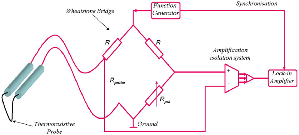
Figure 13. 3ω-scanning thermal microscopy measurement. Reprint with permission from Grauby et al. (2013). Copyright 2013 American Chemical Society.
TE Properties for NWs and TEG
The first measured thermal conductivity of silicon NWs was achieved in 2003, and found a small value of κ down to 7–8 W m−1 K−1 for NWs 22 nm wide with the VLS method (Li et al., 2003b). Compared to 20 nm thickness Si film with thermal conductivity ~ 22 W m−1 K−1, a reduction of around two-thirds of the thermal conductivity was observed, and the value becomes smaller than measured suspended films down to a thickness of ~10 nm with thermal conductivity ~10 W m−1 K−1. For the measurement, they used microfabricated suspended plates for the positioning of the individual NW, where Pt resistors were integrated in the TEG as electrodes, heater, and thermometer; this method has been adopted in many studies. Following, Hochbaum et al. used 50 nm NWs fabricated by MaCE and demonstrated a very small κ of 1.6 W m−1 K−1 where the phonon thermal conductivity κph was estimated about 1 W m−1 K−1. This is 5–8 times lower than the corresponding Si NWs synthesized by the VLS method (Hochbaum et al., 2008). The reduction was explained by the phonon surface scattering effect, since MaCE NWs exhibited a rougher surface compared to VLS NWs (Pennelli, 2015). Later, more research reports about Si NWs have reported the thermal conductivity based on different equipment. A TE module based on vertical rough Si NWs with 200 nm diameter showed the lowest thermal conductivity between 10.1 and 14.8 W m−1 K−1 with boron- and phosphorus-doped, and the Pmax was 3.74 μW/cm2 with temperature difference ΔT = 180 K (Lee et al., 2019). For different fabrications and measurement techniques, the precision in data varies according to the literature. And the experiment conditions are constantly changing and errors may exist. When measuring the samples, it is crucial to select appropriate measurements for accuracy.
For the fabricated μTEG in research, there are several experimental data of generated output. A vertical Si NW structure is demonstrated by RIE with a TE power of 29.3 μW at ΔT = 56 K under 50 × 50 μm chip area; spin-on glass thin film is applied for the support of Si NW (Curtin et al., 2012). An output power density of 9 μW/cm2 is measured at ΔT = 27 K cross the Si NWs μTEG fabricated by the CVD-VLS methods (Dávila et al., 2012). By standard CMOS processing, 20 thin Si membranes generated an output power density of 4.5 μW/cm2 under ΔT = 5 K by using 20 thin Si membranes made μTEG with area of 50 × 150 μm on the chip (Perez-Marín et al., 2014). More recently, Donmez et al. have measured the maximum power densities of Si NWs, SiGe NWs, and Si micro-beam-based μTEG with values of 41.2, 45.2, and 34.5 μW/ cm2, respectively, at a hot plate temperature of 100°C (Donmez Noyan et al., 2019). A two-leg μTEG has been fabricated based on vertical Si NW forest where the achieved power output is 0.25–0.5 μW/(cm2K2) with the NW length from 25 to 6.5 μm (Elyamny et al., 2020). By shortening Si NW to sub-μm length, a planar μTEG achieved the power density of 12 μW/cm2 with ΔT = 5 K (Tomita et al., 2018b).
Simulations and analytic models based on the finite element method (FEM) have been applied for the risk/cost reduction in fabrication, and the data are compared with the experimental results (Tomita et al., 2018b; Donmez Noyan et al., 2019; Elyamny et al., 2020). In a recent study, with the 3-D FEM device simulation software COMSOL Multiphysics, a research group has analyzed the thermal distribution and power generation of Si NWs TEG with varied parameters (Zhang et al., 2018). An extreme high-power density of 4.2 and 425 mW/cm2 was achieved in the simulation at 0.1 × 0.1 μm Si NWs, respectively, under ΔT = 5 and 57 K. With the model, maximum power generation density is speculated to be proportional to ΔT2.
Thermal and Electrical Contact Resistance
The electrical and thermal contact resistance of the metal electrodes are special issues for measurement which have severe impacts on the nanodevice performance which mean that ohmic contacts are necessary. Following the scaling of IC-technology, different metal electrodes have been experimented on for the contact resistance with the tendency of TiSi2 → CoSi2 → Ni(Pt)Si in planar structures (Lavoie et al., 2017). For the fabrication of μTEG integrated with a heater, Pt is a good choice for both electrodes and heaters due to its thermal-independence and low electrical/thermal contact resistance (Noroozi et al., 2017b). NiSi has also been a good choice for electrodes for those μTEG heated from the outside (Zhan et al., 2018). AlN films are adopted as thermally conductive layers for TEG with 300/500 nm thickness and the respective thermal conductivity is 4 and 11 W m−1 K−1. Other metals or multi-metals have been adopted, like tungsten (W) (Gadea Díez et al., 2020), Ti/W (Noyana et al., 2019), Ti/Pt (Boukai et al., 2008), and so forth. Recent research has reported the effect of thermal boundary resistance in the contact layer, and several metal/adhesion/dielectric materials have been compared for their thermal conduct property. The contact layer with the Al/Ti/SiO2 (300/10/10 nm) structure turns out to have the best TE performance compared to the counterpart Cu/Cr/AlN (Zhan et al., 2020). Furthermore, a study found that it is effective in reducing the heat loss across the interfaces by utilizing Ag foil as electrodes and exerting pressure on it (Xu et al., 2013). They also found that, by applying spin-on-doping (SOD) on the Si wafers before the NW arrays are etched, the electrical contact resistance can be reduced by the heavily doped top of NWs. By searching for the optimal power output, an original zigzag arrangement has been implemented for metal supports which allows aligned membranes with arbitrary length. Due to the enhanced metal/window area ratio, such a structure can provide decreased internal resistances (Calaza et al., 2016).
Other than Si NW metallic contact, researchers have also investigated the contact for SiGe. Cobalt has been used to form the CoSi2 on the SiGe layer (Nur et al., 1994, 1995). Nickel has been applied to the SiGe with carbon doping and the thermal stability of Ni(SiGeC) is improved compared with Ni(SiGe) (Hållstedt et al., 2004). A similar thermal stability enhancement by carbon doping has also been observed in Ni(Ge) and Ni(GeSn) (Liu et al., 2014, 2015). Moreover, instead of traditional TiSi2, TiSix, and TiSixGey are used for the Ti-based ohmic contacts (Mao et al., 2017; Mao and Luo, 2019).
Ideal contact materials should have the following characteristics: (1) higher electrical and thermal conductivity than TE material, (2) the coefficient of thermal expansion(CTE) of the material is matched with the TE elements, (3) the deposited layer can be very thin for the reduction of contact resistances, (4) low interface resistance, (5) high stability for the working temperature, (6) stronger yield strength at operating temperature, and (7) good mechanical bonding with the TE layer (Liu W. et al., 2015; He et al., 2018).
Design and Application of μTEG
μTEG Design
Unlike the traditional TEG with a large size, μTEG commonly works at small temperature differences for its small dimension and severer parasitic electrical/thermal resistances. These should be considered in the design of μTEG and its packaging. According to the different structures, the μTEG was classified into three types as follows (Yan et al., 2018).
Type 1—vertical structure (out-of-plane): μTEG with both vertical heat and current flow in Figure 14A.
Type 2—lateral structure (in-plane/planar): μTEG with both lateral heat and current flow in Figure 14B.
Type 3—hybrid structure: TEG with vertical heat and lateral current flow in Figure 14C.
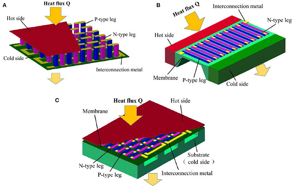
Figure 14. Three types of μTEG. (A) Vertical structure; (B) lateral structure; (C) hybrid structure. Reprint with permission from Yan et al. (2018).
Fabricated with sandwich structure, the vertical TEG was the traditional structure of μTEG and widely utilized in commercial TE devices. Recently, a series of vertical Si NWs modules and TEGs have been fabricated (Curtin et al., 2012; Tomita et al., 2018a; Lee et al., 2019). Generally, μTEGs with this structure are easy to design, and they have large output power and high conversion efficiency. However, the defects come from the difficult and expensive fabrication process, like the deep-etching in the top-down methods, or the well-controlled NW synthesis and metal electrodes integration in the bottom-up methods (Zhan et al., 2018). The lateral structure μTEG, which is compatible with the CMOS process, is relatively easy to fabricate (Xie et al., 2010; Yu et al., 2012, 2015; Noroozi et al., 2017b). But the drawbacks lie in the comparatively low efficiency owing to high parasitic heat flux and low temperature difference. For that reason, the lateral structure is unable to be utilized in power generation and often applied in different sensors. As a compromise of the abovementioned two structures, the hybrid structure shows integrated advantages. In the hybrid structure, the heat flux from ambient flows vertically in a planar direction, and is ejected vertically from another side (Xie et al., 2010). Therefore, the hybrid structure μTEG is desirable to satisfy particular applications and the key for the optimization is the design of a heat flux path.
Moreover, the substrates are etched away to form thermally isolated Si NWs for high efficacy, resulting in a vulnerable structure and expensive fabrication cost. Generally, the high conversion efficiency is essential when the expensive specified heat source is applied, such as RTG, while power generation density is crucial for the heat source which is cheap or free, like waste heat (Zhan et al., 2018).
Performance and Application
In fact, the first generation of TEG, the radioisotope TEG, has been used during the last four decades for power supply by converting the thermal power generated by a radioisotope heat source to electricity for many planetary exploration missions. Unlike a solar power generator, the RTG can operate without sunlight. That advantage fits well with long (more than 10 years) and far-distanced missions (O'Brien et al., 2008).
The μTEGs are a terrific power source for existing and coming electronics considering their ubiquity, magnitude of heat dissipation, and the direct, stable, and non-pollutive energy conversion. The aim of μTEG research is to supply steady electricity power for those miniature electronic instruments. A comparison of the existing microgenerators and applications has been exhibited in Figure 15 (Iannacci, 2019). After the research into TEG and boom of electrical technology, μTEGs have come to be utilized in many fields, like business electronics, health electronics, and IoT (Haras and Skotnicki, 2018; Tomita et al., 2018a). For business electronics, the milestone application of μTEG was a TE watch named Thermatron which was introduced by Bulova in 1980; however it failed due to its unreliable battery and high price (Adams, 2019). A recent smart watch named Matrix Powerwatch II, which is powered by body temperature, has the like calorie counting, sleep tracker, and step counting (Powerwatch, 2020).
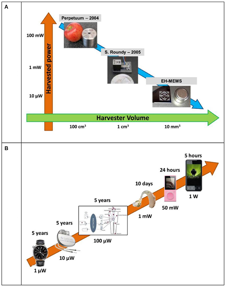
Figure 15. (A) Exsiting microgenerator; (B) Typical low-power devices. Reprint from Iannacci (2019).
Heat dissipation from the human body has been considered as an excellent source of heat energy. As the skin on the wrist has a relatively constant temperature of 36.5°C, it would be possible to utilize this heat for wearable TEGs (Lv et al., 2016). Meanwhile, the temperature difference between the skin and the internal body can reach a maximum of 8°C, sufficient to generate a microwatt level of electricity with μTEG (Ben Amar et al., 2015). It can serve as an alternative power supply compared to other conventional power sources in many wearable devices, especially with implant medical devices like pacemakers (Siddique et al., 2017). For IMD, the difficulty is the permanent operation or standby of the electronics with no secondary removal; body heat is a perfect endless source for those devices like pacemakers.
The increase of research into IoT has also promoted the application of μTEG. The IoT calls for smart, integrated, miniaturized, and low-energy wireless nodes, powered by non-renewable batteries in most cases. The most important part of IoT is the discrete wireless sensor networks (WSNs) which are distributed in different fields like intelligent buildings, medical treatment, monitoring, and security (Ghayvat et al., 2015). The low power dissipation (10–104 μW/cm2) corresponds with the power supplied by μTEG (Noyana et al., 2019). A TE energy harvesting system for WSN has been designed with an input power of 84 μW (Guan et al., 2017). Designed for building energy management (BEM), a TEG-powered WSNs module has been built and characterized in a recent study, which shows the possibility for further application of μTEG for WSNs (Wang et al., 2013).
Some problems limited the application for μTEG and need better solutions. Above all, the conversion efficiency of energy is around 5–10% owing to the low ZT of TE materials (mostly <1), which is much lower than traditional generators and has no market competitiveness. Secondly, it is difficult to attain high temperature differences in daily life; for a wearable TEG, the typical ΔT is 5–15°C. Finally, a suitable external load is needed for load matching and power matching (Siddique et al., 2017). More requirements of TEG can be illustrated by Figure 16, which is also essential for μTEG. A good TE power system should possess all three demands as a minimum: efficiency, effectiveness, and reliability (Liu W. et al., 2015). More detailed requirements should be considered like strong device bonding strength, excellent thermal stability, and chemical stability.
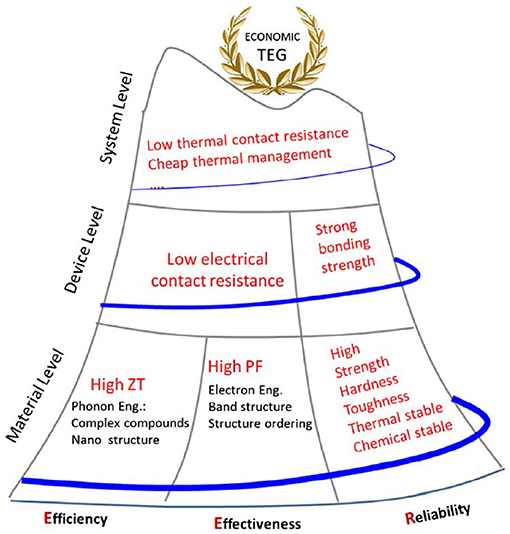
Figure 16. Hierarchical requirements for TEG: the efficiency–effectiveness–reliability mountain. Reprint from Liu W. et al. (2015).
Summary and Prospect
In this review article, we have explored the basic conceptions in the fabrication of Si-based NW μTEG. The μTEG has a bright future as an efficient method for power supply in wireless microelectronic devices due to its energy recycle and convenience. However, there are still many problems that must be addressed before proceeding to large-scale application. Among those TE properties that influence ZT, thermal conductivity κ is the most important parameter in the consideration for the design of μTEG with Si and SiGe NWs. Most research is focusing on the tuning of phonon thermal conductivity, which is dominant in semiconductors. Then the novel potential materials in Group IV have been stated; specifically we explain the superiority of Si and SiGe NWs as a candidate for TEs. Simple examples for the novel structure in the SiGe NWs e.g., superlattice (SL), core-shell (C-S), etc., have been presented for their possibility to further enhance the TE properties. The methods for fabrication are also introduced in this article, with the top-down and bottom-up methods illustrated and the detailed process generalized like MBE, RIE, and STL. After the process, the analysis and characterization of TE in different articles about the TE parameters are reviewed here, the commonly used 4-point probing for the electrical properties with I-V characteristic curve described and 3ω method for the thermal conductivity. Finally, we describe the existing and prospective applications for TEG-sourced devices, which are likely to be an enormous market in the near future. For the utilization of μTEG, IoT is a good carrier due to its miniature energy consumption. Also, flexible wearable devices and implantable medical devices are promising directions.
We believe more research is necessary to further enhance the TE properties and lower the cost of processing and power generating. From this research, Si and SiGe NW μTEGs have the potential to find their niche in daily life and in more complicated application scenarios.
Author Contributions
YL and HR conceived and designed the manuscript. YL wrote the article. GW, MA-S, MP, and HR revised it. All authors contributed to the article and approved the submitted version.
Funding
This work was supported by the construction of high-level innovation research institute from the Guangdong Greater Bay Area Institute of Integrated Circuit and System (Grant No. 2019B090909006) and the projects of the construction of new research and development institutions (Grant No. 2019B090904015), in part by the the National Key Research and Development Program of China (Grant No. 2016YFA0301701), the Youth Innovation Promotion Association of CAS (Grant No. Y2020037), and the National Natural Science Foundation of China (Grant No. 92064002).
Conflict of Interest
The authors declare that the research was conducted in the absence of any commercial or financial relationships that could be construed as a potential conflict of interest.
Acknowledgments
Financial support from the Institute of Microelectronics, Chinese Academic of Science and Guangdong Greater Bay Area Institute of Integrated Circuit and System is gratefully acknowledged.
References
Abad, B., Borca-Tasciuc, D. A., and Martin-Gonzalez, M. S. (2017). Non-contact methods for thermal properties measurement. Renew. Sustain. Energy Rev. 76, 1348–1370. doi: 10.1016/j.rser.2017.03.027
Adams, A. (2019). Bulova Thermatron Watch Hands-On: The Temperature-Powered Timepiece That Never Was. Available online at: https://www.ablogtowatch.com/bulova-thermatron-watch-temperature-powered-timepiece/
Akbari-Saatlu, M., Procek, M., Mattsson, C., Thungstrom, G., Nilsson, H. E., Xiong, W., et al. (2020). Silicon nanowires for gas sensing: a review. Nanomaterials 10:2215. doi: 10.3390/nano10112215
Bahk, J.-H., Bian, Z., and Shakouri, A. (2013). Electron energy filtering by a nonplanar potential to enhance the thermoelectric power factor in bulk materials. Phys. Rev. B 87:075204. doi: 10.1103/PhysRevB.87.075204
Barraud, S., Previtali, B., Lapras, V., Coquand, R., Vizioz, C., Hartmann, J. M., et al. (2019). Top-down fabrication and electrical characterization of Si and SiGe nanowires for advanced CMOS technologies. Semicond. Sci. Technol. 34:074001. doi: 10.1088/1361-6641/ab1e5b
Ben Amar, A., Kouki, A. B., and Cao, H. (2015). Power approaches for implantable medical devices. Sensors 15, 28889–28914. doi: 10.3390/s151128889
Bennett, N. S., Byrne, D., and Cowley, A. (2015). Enhanced Seebeck coefficient in silicon nanowires containing dislocations. Appl. Phys. Lett. 107:013903. doi: 10.1063/1.4926331
Borup, K. A., de Boor, J., Wang, H., Drymiotis, F., Gascoin, F., Shi, X., et al. (2015). Measuring thermoelectric transport properties of materials. Energy Environ. Sci. 8, 423–435. doi: 10.1039/C4EE01320D
Boukai, A. I., Bunimovich, Y., Tahir-Kheli, J., Yu, J. K., Goddard, W. A. III., and Heath, J. R. (2008). Silicon nanowires as efficient thermoelectric materials. Nature 451, 168–171. doi: 10.1038/nature06458
Cahill, D. G. (1990). Thermal conductivity measurement from 30 to 750 K: the 3ω method. Rev. Scient. Instrum. 61, 802–808. doi: 10.1063/1.1141498
Cahill, D. G., Ford, W. K., Goodson, K. E., Mahan, G. D., Majumdar, A., Maris, H. J., et al. (2003). Nanoscale thermal transport. J Appl Phys. 93, 793–818. doi: 10.1063/1.1524305
Calaza, C., Donmez, I., Salleras, M., Gadea, G., Santos, J. D., Morata, A., et al. (2016). Optimization of power output in planar thermoelectric microgenerators based on Si nanowires. J. Phys. Conf. Ser. 773:012026. doi: 10.1088/1742-6596/773/1/012026
Calaza, C., Salleras, M., Dávila, D., Tarancón, A., Morata, A., Santos, J. D., et al. (2015). Bottom-up silicon nanowire arrays for thermoelectric harvesting. Mater. Today Proc. 2, 675–679. doi: 10.1016/j.matpr.2015.05.085
Chen, J., Zhang, G., and Li, B. (2009). Tunable thermal conductivity of Si1−xGex nanowires. Appl. Phys. Lett. 95:073117. doi: 10.1063/1.3212737
Chen, R., Lee, J., Lee, W., and Li, D. (2019). Thermoelectrics of nanowires. Chem. Rev. 119, 9260–9302. doi: 10.1021/acs.chemrev.8b00627
Chen, S., Li, W., Li, X., and Yang, W. (2019). One-dimensional SiC nanostructures: designed growth, properties, and applications. Prog. Mater. Sci. 104, 138–214. doi: 10.1016/j.pmatsci.2019.04.004
Chen, X., Wang, Y., and Ma, Y. (2010). High thermoelectric performance of Ge/Si core–shell nanowires: first-principles prediction. J. Phys. Chem. C 114, 9096–9100. doi: 10.1021/jp101132u
Chen, X., Wang, Z., and Ma, Y. (2011). Atomistic design of high thermoelectricity on Si/Ge superlattice nanowires. J. Phys. Chem. C 115, 20696–20702. doi: 10.1021/jp2060014
Choi, J. H., Pala, M., Latu-Romain, L., and Bano, E. (2011). Theoretical study of thermoelectric properties of SiC nanowires. Mater. Sci. Forum. 717–720, 561–564. doi: 10.4028/www.scientific.net/MSF.717-720.561
Chou, Y. C., Wen, C. Y., Reuter, M. C., Su, D., Stach, E. A., and Ross, F. M. (2012). Controlling the growth of Si/Ge nanowires and heterojunctions using silver-gold alloy catalysts. ACS Nano. 6, 6407–6415. doi: 10.1021/nn301978x
Curtin, B. M., and Bowers, J. E. (2014). Thermoelectric power factor enhancement with gate-all-around silicon nanowires. J. Appl. Phys. 115:143704. doi: 10.1063/1.4870962
Curtin, B. M., Fang, E. W., and Bowers, J. E. (2012). Highly ordered vertical silicon nanowire array composite thin films for thermoelectric devices. J. Electron. Mater. 41, 887–894. doi: 10.1007/s11664-012-1904-1
Dames, C., and Chen, G. (2004). Theoretical phonon thermal conductivity of Si/Ge superlattice nanowires. J. Appl. Phys. 95, 682–693. doi: 10.1063/1.1631734
David, T., Liu, K., Ronda, A., Favre, L., Abbarchi, M., Gailhanou, M., et al. (2017). Tailoring strain and morphology of core-shell SiGe nanowires by low-temperature Ge condensation. Nano Lett. 17, 7299–7305. doi: 10.1021/acs.nanolett.7b02832
Dávila, D., Tarancón, A., Calaza, C., Salleras, M., Fernández-Regúlez, M., San Paulo, A., et al. (2012). Monolithically integrated thermoelectric energy harvester based on silicon nanowire arrays for powering micro/nanodevices. Nano Energy 1, 812–819. doi: 10.1016/j.nanoen.2012.06.006
de Boor, J., Geyer, N., Wittemann, J. V., Gosele, U., and Schmidt, V. (2010). Sub-100 nm silicon nanowires by laser interference lithography and metal-assisted etching. Nanotechnology 21:095302. doi: 10.1088/0957-4484/21/9/095302
Donmez Noyan, I., Dolcet, M., Salleras, M., Stranz, A., Calaza, C., Gadea, G., et al. (2019). All-silicon thermoelectric micro/nanogenerator including a heat exchanger for harvesting applications. J. Power Sources 413, 125–133. doi: 10.1016/j.jpowsour.2018.12.029
Dresselhaus, M. S., Chen, G., Tang, M. Y., Yang, R. G., Lee, H., Wang, D. Z., et al. (2007). New directions for low-dimensional thermoelectric materials. Adv. Mater. 19, 1043–1053. doi: 10.1002/adma.200600527
Elyamny, S., Dimaggio, E., Magagna, S., Narducci, D., and Pennelli, G. (2020). High power thermoelectric generator based on vertical silicon nanowires. Nano Lett. 20, 4748–4753. doi: 10.1021/acs.nanolett.0c00227
Feser, J. P., Sadhu, J. S., Azeredo, B. P., Hsu, K. H., Ma, J., Kim, J., et al. (2012). Thermal conductivity of silicon nanowire arrays with controlled roughness. J. Appl. Phys. 112:114306. doi: 10.1063/1.4767456
Gadea Díez, G., Sojo Gordillo, J. M., Pacios Pujadó, M., Salleras, M., Fonseca, L., Morata, A., et al. (2020). Enhanced thermoelectric figure of merit of individual Si nanowires with ultralow contact resistances. Nano Energy 67:104191. doi: 10.1016/j.nanoen.2019.104191
Gadea, G., Morata, A., and Tarancon, A. (2018a). Semiconductor nanowires for thermoelectric generation. Semiconduct. Semimetals 98, 321–407. doi: 10.1016/bs.semsem.2018.01.001
Gadea, G., Pacios, M., Morata, Á., and Tarancón, A. (2018b). Silicon-based nanostructures for integrated thermoelectric generators. J. Phys. D Appl. Phys. 51:423001. doi: 10.1088/1361-6463/aad683
Garg, J., Bonini, N., Kozinsky, B., and Marzari, N. (2011). Role of disorder and anharmonicity in the thermal conductivity of silicon-germanium alloys: a first-principles study. Phys. Rev. Lett. 106:045901. doi: 10.1103/PhysRevLett.106.045901
Geyer, N., Huang, Z., Fuhrmann, B., Grimm, S., Reiche, M., Nguyen-Duc, T. K., et al. (2009). Sub-20 nm Si/Ge superlattice nanowires by metal-assisted etching. Nano Lett. 9, 3106–3110. doi: 10.1021/nl900751g
Ghayvat, H., Mukhopadhyay, S., Gui, X., and Suryadevara, N. (2015). WSN- and IOT-based smart homes and their extension to smart buildings. Sensors 15, 10350–10379. doi: 10.3390/s150510350
Glassbrenner, C. J., and Slack, G. A. (1964). Thermal conductivity of silicon and germanium from 3°K to the melting point. Phys. Rev. 134, A1058–A1069. doi: 10.1103/PhysRev.134.A1058
Goktas, N. I., Wilson, P., Ghukasyan, A., Wagner, D., McNamee, S., and LaPierre, R. R. (2018). Nanowires for energy: a review. Appl. Phys. Rev. 5:041305. doi: 10.1063/1.5054842
Goldsmid, H. J. (2014). Bismuth telluride and its alloys as materials for thermoelectric generation. Materials 7, 2577–2592. doi: 10.3390/ma7042577
Grahn, J. V., Fosshaug, H., Jargelius, M., Jönsson, P., Linder, M., Malm, B. G., et al. (2000). A low-complexity 62-GHz fT SiGe heterojunction bipolar transistor process using differential epitaxy and in situ phosphorus-doped poly-Si emitter at very low thermal budget. Solid State Electron. 44, 549–554. doi: 10.1016/S0038-1101(99)00266-X
Grauby, S., Puyoo, E., Rampnoux, J.-M., Rouvière, E., and Dilhaire, S. (2013). Si and SiGe nanowires: fabrication process and thermal conductivity measurement by 3ω-scanning thermal microscopy. J. Phys. Chem. C 117, 9025–9034. doi: 10.1021/jp4018822
Guan, M., Wang, K., Xu, D., and Liao, W.-H. (2017). Design and experimental investigation of a low-voltage thermoelectric energy harvesting system for wireless sensor nodes. Energy Convers. Manage. 138, 30–37. doi: 10.1016/j.enconman.2017.01.049
Hållstedt, J., Blomqvist, M., Persson, P. O. Å., Hultman, L., and Radamson, H. H. (2004). The effect of carbon and germanium on phase transformation of nickel on Si1−x−yGexCy epitaxial layers. J. Appl. Phys. 95, 2397–2402. doi: 10.1063/1.1645996
Hållstedt, J., Hellström, P. E., and Radamson, H. H. (2008a). Sidewall transfer lithography for reliable fabrication of nanowires and deca-nanometer MOSFETs. Thin Solid Films 517, 117–120. doi: 10.1016/j.tsf.2008.08.134
Hållstedt, J., Kolahdouz, M., Ghandi, R., Radamson, H. H., and Wise, R. (2008b). Pattern dependency in selective epitaxy of B-doped SiGe layers for advanced metal oxide semiconductor field effect transistors. J. Appl. Phys. 103:054907. doi: 10.1063/1.2832631
Haras, M., and Skotnicki, T. (2018). Thermoelectricity for IoT – a review. Nano Energy 54, 461–476. doi: 10.1016/j.nanoen.2018.10.013
Harman, T. C., Taylor, P. J., Walsh, M. P., and LaForge, B. E. (2002). Quantum dot superlattice thermoelectric materials and devices. Science 297, 2229–2232. doi: 10.1126/science.1072886
Hattori, J., and Uno, S. (2013). Impact of isotope doping on phonon thermal transport in silicon nanowires. Jpn. J. Appl. Phys. 52:04CN04. doi: 10.7567/JJAP.52.04CN04
He, R., Schierning, G., and Nielsch, K. (2018). Thermoelectric devices: a review of devices, architectures, and contact optimization. Adv. Mater. Technol. 3:1700256. doi: 10.1002/admt.201700256
Heremans, J. P., Jovovic, V., Toberer, E. S., Saramat, A., Kurosaki, K., Charoenphakdee, A., et al. (2008). Enhancement of thermoelectric efficiency in PbTe by distortion of the electronic density of states. Science 321, 554–557. doi: 10.1126/science.1159725
Hicks, L. D., and Dresselhaus, M. S. (1993a). Thermoelectric figure of merit of a one-dimensional conductor. Phys. Rev. B Condens. Matter. 47, 16631–16634. doi: 10.1103/PhysRevB.47.16631
Hicks, L. D., and Dresselhaus, M. S. (1993b). Effect of quantum-well structures on the thermoelectric figure of merit. Phys. Rev. B Condens. Matter. 47, 12727–12731. doi: 10.1103/PhysRevB.47.12727
Hijazi, M., and Kazan, M. (2016). Phonon heat transport in superlattices: case of Si/SiGe and SiGe/SiGe superlattices. AIP Adv. 6:065024. doi: 10.1063/1.4955052
Hochbaum, A. I., Chen, R., Delgado, R. D., Liang, W., Garnett, E. C., Najarian, M., et al. (2008). Enhanced thermoelectric performance of rough silicon nanowires. Nature 451, 163–167. doi: 10.1038/nature06381
Hu, M., Giapis, K. P., Goicochea, J. V., Zhang, X., and Poulikakos, D. (2011). Significant reduction of thermal conductivity in Si/Ge core-shell nanowires. Nano Lett. 11, 618–623. doi: 10.1021/nl103718a
Huang, Z., Geyer, N., Werner, P., de Boor, J., and Gosele, U. (2011). Metal-assisted chemical etching of silicon: a review. Adv. Mater. Weinheim. 23, 285–308. doi: 10.1002/adma.201001784
Huxtable, S. T., Abramson, A. R., Tien, C.-L., Majumdar, A., LaBounty, C., Fan, X., et al. (2002). Thermal conductivity of Si/SiGe and SiGe/SiGe superlattices. Appl. Phys. Lett. 80, 1737–1739. doi: 10.1063/1.1455693
Iannacci, J. (2019). Microsystem based Energy Harvesting (EH-MEMS): powering pervasivity of the Internet of Things (IoT) – a review with focus on mechanical vibrations. J. King Saud Univ. Sci. 31, 66–74. doi: 10.1016/j.jksus.2017.05.019
Ishibe, T., Tomeda, A., Watanabe, K., Kamakura, Y., Mori, N., Naruse, N., et al. (2018). Methodology of thermoelectric power factor enhancement by controlling nanowire interface. ACS Appl. Mater. Interfaces 10, 37709–37716. doi: 10.1021/acsami.8b13528
Joshi, G., Lee, H., Lan, Y., Wang, X., Zhu, G., Wang, D., et al. (2008). Enhanced thermoelectric figure-of-merit in nanostructured p-type silicon germanium bulk alloys. Nano Lett. 8, 4670–4674. doi: 10.1021/nl8026795
Ju, Y. S., and Goodson, K. E. (1999). Phonon scattering in silicon films with thickness of order 100 nm. Appl. Phys. Lett. 74, 3005–3007. doi: 10.1063/1.123994
June, F., and Zakrajsek, D. F. W. (2017). Jean-Pierre Fleurial NASA Special Session: Next-Generation Radiaisotope Thermoelectric Generator Discussion.
Kandemir, A., Ozden, A., Cagin, T., and Sevik, C. (2017). Thermal conductivity engineering of bulk and one-dimensional Si-Ge nanoarchitectures. Sci. Technol. Adv. Mater. 18, 187–196. doi: 10.1080/14686996.2017.1288065
Kao, P. H., Shih, P. J., Dai, C. L., and Liu, M. C. (2010). Fabrication and characterization of CMOS-MEMS thermoelectric micro generators. Sensors 10, 1315–1325. doi: 10.3390/s100201315
Khatami, S. N., and Aksamija, Z. (2016). Lattice thermal conductivity of the binary and ternary group-IV alloys Si-Sn, Ge-Sn, and Si-Ge-Sn. Phys. Rev. Appl. 6:014015. doi: 10.1103/PhysRevApplied.6.014015
Kim, H., Kim, I., Choi, H.-J., and Kim, W. (2010). Thermal conductivities of Si1−xGex nanowires with different germanium concentrations and diameters. Appl. Phys. Lett. 96:3443707. doi: 10.1063/1.3443707
Kim, H., Park, Y.-H., Kim, I., Kim, J., Choi, H.-J., and Kim, W. (2011). Effect of surface roughness on thermal conductivity of VLS-grown rough Si1−x Ge x nanowires. Appl. Phys. A 104, 23–28. doi: 10.1007/s00339-011-6475-0
Kim, J., Shim, W., and Lee, W. (2015). Bismuth nanowire thermoelectrics. J. Mater. Chem. C 3, 11999–12013. doi: 10.1039/C5TC02886H
Kim, W. (2013). Thermal transport in individual thermoelectric nanowires: a review. Mater. Res. Innov. 15, 375–385. doi: 10.1179/1433075X11Y.0000000046
Kirihara, K., Sasaki, T., Koshizaki, N., and Kimura, K. (2011). Seebeck coefficient and power factor of single-crystalline boron nanobelts. Appl. Phys. Express. 4:041201. doi: 10.1143/APEX.4.041201
Kleinke, H. (2010). New bulk materials for thermoelectric power generation: clathrates and complex antimonides†. Chem. Mater. 22, 604–611. doi: 10.1021/cm901591d
Koumoto, K., Wang, Y., Zhang, R., Kosuga, A., and Funahashi, R. (2010). Oxide thermoelectric materials: a nanostructuring approach. Annu. Rev. Mater. Res. 40, 363–394. doi: 10.1146/annurev-matsci-070909-104521
Kumar, M., Rani, S., Singh, Y., and Singh, V. N. (2020). Tuning the thermoelectric material's parameter: a comprehensive review. J. Nanosci. Nanotechnol. 20, 3636–3646. doi: 10.1166/jnn.2020.17531
Lavoie, C., Adusumilli, P., Carr, A. V., Jordan Sweet, J. S., Ozcan, A. S., Levrau, E., et al. (2017). Contacts in advanced CMOS: history and emerging challenges. ECS Trans. 77, 59–79. doi: 10.1149/07705.0059ecst
Lee, K. M., Choi, T. Y., Lee, S. K., and Poulikakos, D. (2010). Focused ion beam-assisted manipulation of single and double beta-SiC nanowires and their thermal conductivity measurements by the four-point-probe 3-omega method. Nanotechnology 21:125301. doi: 10.1088/0957-4484/21/12/125301
Lee, S., Kim, K., Kang, D. H., Meyyappan, M., and Baek, C. K. (2019). Vertical silicon nanowire thermoelectric modules with enhanced thermoelectric properties. Nano Lett. 19, 747–755. doi: 10.1021/acs.nanolett.8b03822
Lee, S. M., Cahill, D. G., and Venkatasubramanian, R. (1997). Thermal conductivity of Si–Ge superlattices. Appl. Phys. Lett. 70, 2957–2959. doi: 10.1063/1.118755
Lee, Y., and Hwang, G. S. (2017). Molecular dynamics investigation of the thermal conductivity of ternary silicon–germanium–tin alloys. J. Phys. D Appl. Phys. 50:494001. doi: 10.1088/1361-6463/aa94a0
Li, C. B., Xu, B., Durrani, Z. A. K., Mironov, M., and Fobelets, K. (2012). Thermoelectric characteristics of SiGe nanowire arrays as a function of Ge concentration. AIP Conf. Proc. 1449, 417–420. doi: 10.1063/1.4731585
Li, D., Wu, Y., Fan, R., Yang, P., and Majumdar, A. (2003a). Thermal conductivity of Si/SiGe superlattice nanowires. Appl. Phys. Lett. 83, 3186–3188. doi: 10.1063/1.1619221
Li, D., Wu, Y., Kim, P., Shi, L., Yang, P., and Majumdar, A. (2003b). Thermal conductivity of individual silicon nanowires. Appl. Phys. Lett. 83, 2934–2936. doi: 10.1063/1.1616981
Li, Y., Buddharaju, K., Singh, N., Lo, G. Q., and Lee, S. J. (2011). Chip-level thermoelectric power generators based on high-density silicon nanowire array prepared with top-down cmos technology. IEEE Electron Device Lett. 32, 674–676. doi: 10.1109/LED.2011.2114634
Liu, J., Liu, H., Ma, W., and Zhang, X. (2019). Non-contact T-type Raman method for measurement of thermophysical properties of micro-/nanowires. Rev. Scientif. Instrum. 90:044901. doi: 10.1063/1.5080728
Liu, Q., Geilei, W., Guo, Y., Ke, X., Radamson, H., Liu, H., et al. (2014). Improvement of the thermal stability of nickel stanogermanide by carbon pre-stanogermanidation implant into GeSn substrate. ECS J. Solid State Sci. Technol. 4, P67–P70. doi: 10.1149/2.0041503jss
Liu, Q., Wang, G., Duan, N., Radamson, H., Liu, H., Zhao, C., et al. (2015). Effects of carbon pre-germanidation implantation on the thermal stability of NiGe and dopant segregation on both n- and p-type Ge substrate. ECS J. Solid State Sci. Technol. 4, P119–P123. doi: 10.1149/2.0041505jss
Liu, W., Jie, Q., Kim, H. S., and Ren, Z. (2015). Current progress and future challenges in thermoelectric power generation: from materials to devices. Acta Mater. 87, 357–376. doi: 10.1016/j.actamat.2014.12.042
Liu, Y., Zhang, M., Ji, A., Yang, F., and Wang, X. (2016). Measuring methods for thermoelectric properties of one-dimensional nanostructural materials. RSC Adv. 6, 48933–48961. doi: 10.1039/C5RA23634G
Lu, L., Yi, W., and Zhang, D. L. (2001). 3ω method for specific heat and thermal conductivity measurements. Rev. Scient. Instrum. 72, 2996–3003. doi: 10.1063/1.1378340
Lü, X. (2009). Longitudinal thermal conductivity of radial nanowire heterostructures. J. Appl. Phys. 106:064305. doi: 10.1063/1.3223329
Lv, S., He, W., Wang, L., Li, G., Ji, J., Chen, H., et al. (2016). Design, fabrication and feasibility analysis of a thermo-electric wearable helmet. Appl. Therm. Eng. 109, 138–146. doi: 10.1016/j.applthermaleng.2016.08.057
Maire, J., Anufriev, R., Hori, T., Shiomi, J., Volz, S., and Nomura, M. (2018). Thermal conductivity reduction in silicon fishbone nanowires. Sci. Rep. 8:4452. doi: 10.1038/s41598-018-22509-0
Malhotra, A., and Maldovan, M. (2016). Impact of phonon surface scattering on thermal energy distribution of Si and SiGe nanowires. Sci. Rep. 6:25818. doi: 10.1038/srep25818
Mao, S., and Luo, J. (2019). Titanium-based ohmic contacts in advanced CMOS technology. J. Phys. D Appl. Phys. 52:503001. doi: 10.1088/1361-6463/ab3dc9
Mao, S.-J., Xu, J., Wang, G.-L., Luo, J., Duan, N.-Y., Simoen, E., et al. (2017). On the manifestation of Ge Pre-Amorphization Implantation (PAI) in forming ultrathin TiSixfor Ti direct contact on Si in sub-16/14 nm Complementary Metal-Oxide-Semiconductor (CMOS) technology nodes. ECS J. Solid State Sci. Technol. 6, P660–P664. doi: 10.1149/2.0321709jss
Markussen, T. (2012). Surface disordered Ge-Si core-shell nanowires as efficient thermoelectric materials. Nano Lett. 12, 4698–4704. doi: 10.1021/nl302061f
Martin, J., Wang, L., Chen, L., and Nolas, G. S. (2009). Enhanced Seebeck coefficient through energy-barrier scattering in PbTe nanocomposites. Phys. Rev. B 79:115311. doi: 10.1103/PhysRevB.79.115311
Martinez, J. A., Provencio, P. P., Picraux, S. T., Sullivan, J. P., and Swartzentruber, B. S. (2011). Enhanced thermoelectric figure of merit in SiGe alloy nanowires by boundary and hole-phonon scattering. J. Appl. Phys. 110:074317. doi: 10.1063/1.3647575
Mehdizadeh Dehkordi, A., Zebarjadi, M., He, J., and Tritt, T. M. (2015). Thermoelectric power factor: enhancement mechanisms and strategies for higher performance thermoelectric materials. Mater. Sci. Eng. R Rep. 97, 1–22. doi: 10.1016/j.mser.2015.08.001
Min, K. S., and Atwater, H. A. (1998). Ultrathin pseudomorphic Sn/Si and SnxSi1−x/Si heterostructures. Appl. Phys. Lett. 72, 1884–1886. doi: 10.1063/1.121215
Minnich, A. J., Dresselhaus, M. S., Ren, Z. F., and Chen, G. (2009). Bulk nanostructured thermoelectric materials: current research and future prospects. Energy Environ. Sci. 2, 466–479. doi: 10.1039/b822664b
Moore, A. L., Saha, S. K., Prasher, R. S., and Shi, L. (2008). Phonon backscattering and thermal conductivity suppression in sawtooth nanowires. Appl. Phys. Lett. 93:083112. doi: 10.1063/1.2970044
Moss, R. H., Edmonds, J. A., Hibbard, K. A., Manning, M. R., Rose, S. K., van Vuuren, D. P., et al. (2010). The next generation of scenarios for climate change research and assessment. Nature 463, 747–756. doi: 10.1038/nature08823
Mu, X., Wang, L., Yang, X., Zhang, P., To, A. C., and Luo, T. (2015). Ultra-low thermal conductivity in Si/Ge hierarchical superlattice nanowire. Sci. Rep. 5:16697. doi: 10.1038/srep16697
Mukherjee, S., Givan, U., Senz, S., Bergeron, A., Francoeur, S., de la Mata, M., et al. (2015). Phonon engineering in isotopically disordered silicon nanowires. Nano Lett. 15, 3885–3893. doi: 10.1021/acs.nanolett.5b00708
Narducci, D., Frabboni, S., and Zianni, X. (2015). Silicon de novo: energy filtering and enhanced thermoelectric performances of nanocrystalline silicon and silicon alloys. J. Mater. Chem. C 3, 12176–12185. doi: 10.1039/C5TC01632K
Ni, W. X., Ekberg, J. O., Joelsson, K. B., Radamson, H. H., Henry, A., Shen, G. D., et al. (1995). A silicon molecular beam epitaxy system dedicated to device-oriented material research. J. Cryst. Growth. 157, 285–294. doi: 10.1016/0022-0248(95)00326-6
Noguchi, T., Simanullang, M., Xu, Z., Usami, K., Kodera, T., and Oda, S. (2016). Synthesis of Ge/Si core/shell nanowires with suppression of branch formation. Appl. Phys. Express 9:055504. doi: 10.7567/APEX.9.055504
Nolas, G. S., Morelli, D. T., and Tritt, T. M. (1999). Skutterudites: a phonon-glass-electron crystal approach to advanced thermoelectric energy conversion applications. Annu. Rev. Mater. Sci. 29, 89–116. doi: 10.1146/annurev.matsci.29.1.89
Noroozi, M., Hamawandi, B., Jayakumar, G., Zahmatkesh, K., Radamson, H. H., and Toprak, M. S. (2017a). A comparison of power factor in N and P-Type SiGe nanowires for thermoelectric applications. J. Nanosci. Nanotechnol. 17, 1622–1626. doi: 10.1166/jnn.2017.13728
Noroozi, M., Hamawandi, B., Toprak, M. S., and Radamson, H. H. (2014). “Fabrication and thermoelectric characterization of GeSn nanowires,” in 2014 15th International Conference on Ultimate Integration on Silicon (New York, NY: IEEE), 125–128. doi: 10.1109/ULIS.2014.6813914
Noroozi, M., Jayakumar, G., Zahmatkesh, K., Lu, J., Hultman, L., Mensi, M., et al. (2017b). Unprecedented thermoelectric power factor in SiGe nanowires field-effect transistors. ECS J. Solid State Sci. Technol. 6, Q114–Q119. doi: 10.1149/2.0021710jss
Noyana, I. D., Gadea, G., Sallerasa, M., Paciosb, M., Calazaa, C., Stranza, A., et al. (2019). SiGe nanowire arrays based thermoelectric microgenerator. Nano Energy 57, 492–499. doi: 10.1016/j.nanoen.2018.12.050
Nur, O., Willander, M., Hultman, L., Radamson, H. H., Hansson, G. V., Sardela, M. R., et al. (1995). CoSi2/Si1−xGex/Si(001) heterostructures formed through different reaction routes: silicidation-induced strain relaxation, defect formation, and interlayer diffusion. J. Appl. Phys. 78, 7063–7069. doi: 10.1063/1.360411
Nur, O., Willander, M., Radamson, H. H., Sardela, M. R., Hansson, G. V., Petersson, C. S., et al. (1994). Strain characterization of CoSi2/n-Si0.9Ge0.1/p-Si heterostructures. Appl. Phys. Lett. 64, 440–442. doi: 10.1063/1.111122
O'Brien, R. C., Ambrosi, R. M., Bannister, N. P., Howe, S. D., and Atkinson, H. V. (2008). Safe radioisotope thermoelectric generators and heat sources for space applications. J. Nucl. Mater. 377, 506–521. doi: 10.1016/j.jnucmat.2008.04.009
Oh, S. H., van Benthem, K., Molina, S. I., Borisevich, A. Y., Luo, W., Werner, P., et al. (2008). Point defect configurations of supersaturated Au atoms inside Si nanowires. Nano Lett. 8, 1016–1019. doi: 10.1021/nl072670+
Özden, A., Kandemir, A., Ay, F., and Perkgöz, N. K., Sevik, C. (2015). Thermal conductivity suppression in nanostructured silicon and germanium nanowires. J. Electr. Mater. 45, 1594–1600. doi: 10.1007/s11664-015-4127-4
Pan, Y., Hong, G., Raja, S. N., Zimmermann, S., Tiwari, M. K., and Poulikakos, D. (2015). Significant thermal conductivity reduction of silicon nanowire forests through discrete surface doping of germanium. Appl. Phys. Lett. 106:093102. doi: 10.1063/1.4913879
Papanikolaou, N. (2008). Lattice thermal conductivity of SiC nanowires. J. Phys. Condens. Matter. 20:6. doi: 10.1088/0953-8984/20/13/135201
Pécz, B., Yakimova, R., Syväjärvi, M., Lockowandt, C., Radamson, H., Radnóczi, G., et al. (1999). Structural investigation of SiC epitaxial layers grown under microgravity and on-ground conditions. Thin Solid Films. 357, 137–143. doi: 10.1016/S0040-6090(99)00657-4
Peng, S.-W., Shih, P.-J., and Dai, C.-L. (2015). Manufacturing and characterization of a thermoelectric energy harvester using the CMOS-MEMS technology. Micromachines 6, 1560–1568. doi: 10.3390/mi6101439
Pennelli, G. (2014). Review of nanostructured devices for thermoelectric applications. Beilstein J. Nanotechnol. 5, 1268–1284. doi: 10.3762/bjnano.5.141
Pennelli, G. (2015). Top-down fabrication of silicon nanowire devices for thermoelectric applications: properties and perspectives. Eur. Phys. J. B 88:121. doi: 10.1140/epjb/e2015-50638-0
Pennelli, G., Elyamny, S., and Dimaggio, E. (2018). Thermal conductivity of silicon nanowire forests. Nanotechnology 29:505402. doi: 10.1088/1361-6528/aae5b6
Perez-Marín, A. P., Lopeandía, A. F., Abad, L., Ferrando-Villaba, P., Garcia, G., Lopez, A. M., et al. (2014). Micropower thermoelectric generator from thin Si membranes. Nano Energy. 4, 73–80. doi: 10.1016/j.nanoen.2013.12.007
Poudel, B., Hao, Q., Ma, Y., Lan, Y., Minnich, A., Yu, B., et al. (2008). High-thermoelectric performance of nanostructured bismuth antimony telluride bulk alloys. Science 320, 634–638. doi: 10.1126/science.1156446
Powerwatch (2020). Available online at: https://www.cnpowerwatch.com/?page_id=522
Putnam, M. C., Filler, M. A., Kayes, B. M., Kelzenberg, M. D., Guan, Y., Lewis, N. S., et al. (2008). Secondary ion mass spectrometry of vapor-liquid-solid grown, Au-catalyzed, Si wires. Nano Lett. 8, 3109–3113. doi: 10.1021/nl801234y
Qu, X., and Gu, J. (2020). Phonon transport and thermal conductivity of diamond superlattice nanowires: a comparative study with SiGe superlattice nanowires. RSC Adv. 10, 1243–1248. doi: 10.1039/C9RA08520C
Radamson, H., Zhang, Y., He, X., Cui, H., Li, J., Xiang, J., et al. (2017). The challenges of advanced CMOS process from 2D to 3D. Appl. Sci. 7:1047. doi: 10.3390/app7101047
Radamson, H. H., He, X., Zhang, Q., Liu, J., Cui, H., Xiang, J., et al. (2019). Miniaturization of CMOS. Micromachines (Basel). 10:293. doi: 10.3390/mi10050293
Radamson, H. H., and Kolahdouz, M. (2015). Selective epitaxy growth of Si1−xGex layers for MOSFETs and FinFETs. J. Mater. Sci. Mater. Electron. 26, 4584–4603. doi: 10.1007/s10854-015-3123-z
Radamson, H. H., Zhu, H., Wu, Z., He, X., Lin, H., Liu, J., et al. (2020). State of the art and future perspectives in advanced CMOS technology. Nanomaterials (Basel). 10:1555. doi: 10.3390/nano10081555
Radousky, H. B., and Liang, H. (2012). Energy harvesting: an integrated view of materials, devices and applications. Nanotechnology 23:502001. doi: 10.1088/0957-4484/23/50/502001
Ray, S. K., Katiyar, A. K., and Raychaudhuri, A. K. (2017). One-dimensional Si/Ge nanowires and their heterostructures for multifunctional applications-a review. Nanotechnology 28:092001. doi: 10.1088/1361-6528/aa565c
Rogl, G., Grytsiv, A., Rogl, P., Peranio, N., Bauer, E., Zehetbauer, M., et al. (2014). n-Type skutterudites (R,Ba,Yb)yCo4Sb12 (R=Sr, La, Mm, DD, SrMm, SrDD) approaching ZT≈2.0. Acta Mater. 63, 30–43. doi: 10.1016/j.actamat.2013.09.039
Rojo, M. M., Calero, O. C., Lopeandia, A. F., Rodriguez-Viejo, J., and Martin-Gonzalez, M. (2013). Review on measurement techniques of transport properties of nanowires. Nanoscale 5, 11526–11544. doi: 10.1039/c3nr03242f
Ross, F. M., Tersoff, J., and Reuter, M. C. (2005). Sawtooth faceting in silicon nanowires. Phys. Rev. Lett. 95:146104. doi: 10.1103/PhysRevLett.95.146104
Royo, M., and Rurali, R. (2016). Tuning thermal transport in Si nanowires by isotope engineering. Phys. Chem. Chem. Phys. 18, 26262–26267. doi: 10.1039/C6CP04581B
Sandu, G., Avila Osses, J., Luciano, M., Caina, D., Stopin, A., Bonifazi, D., et al. (2019). Kinked silicon nanowires: superstructures by metal-assisted chemical etching. Nano Lett. 19, 7681–7690. doi: 10.1021/acs.nanolett.9b02568
Sansoz, F. (2011). Surface faceting dependence of thermal transport in silicon nanowires. Nano Lett. 11, 5378–5382. doi: 10.1021/nl2029688
Schierning, G. (2014). Silicon nanostructures for thermoelectric devices: a review of the current state of the art. Phys. Status Solid. 211, 1235–1249. doi: 10.1002/pssa.201300408
Shi, L., Yao, D., Zhang, G., and Li, B. (2009). Size dependent thermoelectric properties of silicon nanowires. Appl. Phys. Lett. 95:063102. doi: 10.1063/1.3204005
Shi, L., Yao, D., Zhang, G., and Li, B. (2010). Large thermoelectric figure of merit in Si1−xGex nanowires. Appl. Phys. Lett. 96:173108. doi: 10.1063/1.3421543
Siddique, A. R. M., Mahmud, S., and Heyst, B. V. (2017). A review of the state of the science on wearable thermoelectric power generators (TEGs) and their existing challenges. Renew. Sustain. Energy Rev. 73, 730–744. doi: 10.1016/j.rser.2017.01.177
Sistani, M., Seifner, M. S., Bartmann, M. G., Smoliner, J., Lugstein, A., and Barth, S. (2018). Electrical characterization and examination of temperature-induced degradation of metastable Ge0.81Sn0.19 nanowires. Nanoscale 10, 19443–19449. doi: 10.1039/C8NR05296D
Slack, G. A. (1964). Thermal conductivity of pure and impure silicon, silicon carbide, and Diamond. J. Appl. Phys. 35, 3460–3466. doi: 10.1063/1.1713251
Snyder, G. J., and Toberer, E. S. (2008). Complex thermoelectric materials. Nat. Mater. 7, 105–114. doi: 10.1038/nmat2090
Steele, M. C., and Rosi, F. D. (1958). Thermal conductivity and thermoelectric power of germanium-silicon alloys. J. Appl. Phys. 29, 1517–1520. doi: 10.1063/1.1722984
Stranz, A., Waag, A., and Peiner, E. (2011). Thermal characterization of vertical silicon nanowires. J. Mater. Res. 26, 1958–1962. doi: 10.1557/jmr.2011.60
Strasser, M., Aigner, R., Lauterbach, C., Sturm, T. F., Franosch, M., and Wachutka, G. (2004). Micromachined CMOS thermoelectric generators as on-chip power supply. Sens. Actuat. A Phys. 114, 362–370. doi: 10.1016/j.sna.2003.11.039
Swinkels, M. Y., and Zardo, I. (2018). Nanowires for heat conversion. J. Phys. D Appl. Phys. 51:353001. doi: 10.1088/1361-6463/aad25f
Takabatake, T., Suekuni, K., Nakayama, T., and Kaneshita, E. (2014). Phonon-glass electron-crystal thermoelectric clathrates: experiments and theory. Rev. Mod. Phys. 86, 669–716. doi: 10.1103/RevModPhys.86.669
Termentzidis, K., Barreteau, T., Ni, Y., Merabia, S., Zianni, X., Chalopin, Y., et al. (2013). Modulated SiC nanowires: molecular dynamics study of their thermal properties. Phys. Rev. B 87:125410. doi: 10.1103/PhysRevB.87.125410
Thesberg, M., Kosina, H., and Neophytou, N. (2016). On the effectiveness of the thermoelectric energy filtering mechanism in low-dimensional superlattices and nano-composites. J. Appl. Phys. 120:234302. doi: 10.1063/1.4972192
Tomita, M., Oba, S., Himeda, Y., Yamato, R., Shima, K., Kumada, T., et al. (2018a). Modeling, simulation, fabrication, and characterization of a 10μW/cm2 class Si-nanowire thermoelectric generator for IoT applications. IEEE Trans. Electron Devices. 65, 5180–5188. doi: 10.1109/TED.2018.2867845
Tomita, M., Oba, S., Himeda, Y., Yamato, R., Shima, K., Kumada, T., et al. (2018b). “10μW/cm2-class high power density planar Si-nanowire thermoelectric energy harvester compatible with CMOS-VLSI Technology,” in 2018 IEEE Symposium on VLSI Technology (Honolulu, HI), 93–94. doi: 10.1109/VLSIT.2018.8510659
Tritt, T. M. (2011). Thermoelectric phenomena, materials, and applications. Annu. Rev. Mater. Res. 41, 433–448. doi: 10.1146/annurev-matsci-062910-100453
Valentín, L. A., Betancourt, J., Fonseca, L. F., Pettes, M. T., Shi, L., Soszyński, M., et al. (2013). A comprehensive study of thermoelectric and transport properties of β-silicon carbide nanowires. J. Appl. Phys. 114:184301. doi: 10.1063/1.4829924
Wagner, R. S., and Ellis, W. C. (1964). Vapor-liquid-solid mechanism of single crystal growth. Appl. Phys. Lett. 4, 89–90. doi: 10.1063/1.1753975
Wang, N., Cai, Y., and Zhang, R. Q. (2008b). Growth of nanowires. Mater. Sci. Eng. R Rep. 60, 1–51. doi: 10.1016/j.mser.2008.01.001
Wang, W., Cionca, V., Wang, N., Hayes, M., O'Flynn, B., and O'Mathuna, C. (2013). Thermoelectric energy harvesting for building energy management wireless sensor networks. Int. J. Distrib. Sens. Netw. 9:232438. doi: 10.1155/2013/232438
Wang, X. W., Lee, H., Lan, Y. C., Zhu, G. H., Joshi, G., Wang, D. Z., et al. (2008a). Enhanced thermoelectric figure of merit in nanostructured n-type silicon germanium bulk alloy. Appl. Phys. Lett. 93:193121. doi: 10.1063/1.3027060
Wang, Z., and Mingo, N. (2010). Diameter dependence of SiGe nanowire thermal conductivity. Appl. Phys. Lett. 97:101903. doi: 10.1063/1.3486171
Wingert, M. C., Chen, Z. C., Dechaumphai, E., Moon, J., Kim, J. H., Xiang, J., et al. (2011). Thermal conductivity of Ge and Ge-Si core-shell nanowires in the phonon confinement regime. Nano Lett. 11, 5507–5513. doi: 10.1021/nl203356h
Wolfsteller, A., Geyer, N., Nguyen-Duc, T. K., Das Kanungo, P., Zakharov, N. D., Reiche, M., et al. (2010). Comparison of the top-down and bottom-up approach to fabricate nanowire-based silicon/germanium heterostructures. Thin Solid Films. 518, 2555–2561. doi: 10.1016/j.tsf.2009.08.021
Wongprakarn, S., Pinitsoontorn, S., Tanusilp, S.-A., and Kurosaki, K. (2018). Enhancing thermoelectric properties of p-type SiGe alloy through optimization of carrier concentration and processing parameters. Mater. Sci. Semiconduct. Process. 88, 239–249. doi: 10.1016/j.mssp.2018.08.020
Wu, R., Zhou, K., Yue, C. Y., Wei, J., and Pan, Y. (2015). Recent progress in synthesis, properties and potential applications of SiC nanomaterials. Prog. Mater. Sci. 72, 1–60. doi: 10.1016/j.pmatsci.2015.01.003
Wu, Y., Fan, R., and Yang, P. (2002). Block-by-block growth of single-crystalline Si/SiGe superlattice nanowires. Nano Lett. 2, 83–86. doi: 10.1021/nl0156888
Xie, G., Guo, Y., Wei, X., Zhang, K., Sun, L., Zhong, J., et al. (2014). Phonon mean free path spectrum and thermal conductivity for Si1−xGex nanowires. Appl. Phys. Lett. 104:233901. doi: 10.1063/1.4882083
Xie, J., Lee, C., and Feng, H. (2010). Design, fabrication, and characterization of CMOS MEMS-based thermoelectric power generators. J. Microelectromech. Syst. 19, 317–324. doi: 10.1109/JMEMS.2010.2041035
Xiong, S., Kosevich, Y. A., Sääskilahti, K., Ni, Y., and Volz, S. (2014). Tunable thermal conductivity in silicon twinning superlattice nanowires. Phys. Rev. B 90:195439. doi: 10.1103/PhysRevB.90.195439
Xu, B., Li, C., Myronov, M., and Fobelets, K. (2013). n-Si–p-Si1−xGex nanowire arrays for thermoelectric power generation. Solid State Electron. 83, 107–112. doi: 10.1016/j.sse.2013.01.038
Yakimova, R., Syväjärvi, M., Lockowandt, C., Linnarsson, M. K., Radamson, H. H., and Janzén, E. (2011). Silicon carbide grown by liquid phase epitaxy in microgravity. J. Mater. Res. 13, 1812–1815. doi: 10.1557/JMR.1998.0256
Yan, J., Liao, X., Yan, D., and Chen, Y. (2018). Review of Micro thermoelectric generator. J. Microelectromech. Syst. 27, 1–18. doi: 10.1109/JMEMS.2017.2782748
Yanagisawa, R., Tsujii, N., Mori, T., Ruther, P., Paul, O., and Nomura, M. (2020). Nanostructured planar-type uni-leg Si thermoelectric generators. Appl. Phys. Express. 13:095001. doi: 10.35848/1882-0786/aba5c4
Yang, J., and Caillat, T. (2011). Thermoelectric materials for space and automotive power generation. MRS Bull. 31, 224–229. doi: 10.1557/mrs2006.49
Yang, K., Cantarero, A., Rubio, A., and D'Agosta, R. (2015). Optimal thermoelectric figure of merit of Si/Ge core-shell nanowires. Nano Res. 8, 2611–2619. doi: 10.1007/s12274-015-0766-2
Yang, L., and Minnich, A. J. (2017). Thermal transport in nanocrystalline Si and SiGe by ab initio based Monte Carlo simulation. Sci. Rep. 7:44254. doi: 10.1038/srep44254
Yang, N., Zhang, G., and Li, B. (2008). Ultralow thermal conductivity of isotope-doped silicon nanowires. Nano Lett. 8, 276–280. doi: 10.1021/nl0725998
Yi, S.-I., and Yu, C. (2015). Modeling of thermoelectric properties of SiGe alloy nanowires and estimation of the best design parameters for high figure-of-merits. J. Appl. Phys. 117:035105. doi: 10.1063/1.4906226
Yu, K., Zhou, Y., Liu, Y., Liu, F., Hu, L., Ao, W., et al. (2019). Near-room-temperature thermoelectric materials and their application prospects in geothermal power generation. Geomech. Geophys. GeoEnergy GeoResour. 6:12. doi: 10.1007/s40948-019-00134-z
Yu, X., Wang, Y., Liu, Y., Li, T., Zhou, H., Gao, X., et al. (2012). CMOS MEMS-based thermoelectric generator with an efficient heat dissipation path. J. Micromech. Microeng. 22:105011. doi: 10.1088/0960-1317/22/10/105011
Yu, X., Xu, D., Liu, Y., Zhou, H., Wang, Y., Gao, X., et al. (2015). Significant performance improvement for micro-thermoelectric energy generator based on system analysis. Int. J. Electr. Power Energy Syst. 67, 417–422. doi: 10.1016/j.ijepes.2014.12.039
Zeier, W. G., Schmitt, J., Hautier, G., Aydemir, U., Gibbs, Z. M., Felser, C., et al. (2016). Engineering half-Heusler thermoelectric materials using Zintl chemistry. Nat. Rev Mater. 1:16032. doi: 10.1038/natrevmats.2016.32
Zekentes, K., and Rogdakis, K. (2011). SiC nanowires: material and devices. J. Phys. D Appl. Phys. 44:133001. doi: 10.1088/0022-3727/44/13/133001
Zhan, T., Ma, S., Jin, Z., Takezawa, H., Mesaki, K., Tomita, M., et al. (2020). Effect of the thermal boundary resistance in metal/dielectric thermally conductive layers on power generation of silicon nanowire microthermoelectric generators. ACS Appl. Mater. Interfaces 12, 34441–34450. doi: 10.1021/acsami.0c09253
Zhan, T., Yamato, R., Hashimoto, S., Tomita, M., Oba, S., Himeda, Y., et al. (2018). Miniaturized planar Si-nanowire micro-thermoelectric generator using exuded thermal field for power generation. Sci. Technol. Adv. Mater. 19, 443–453. doi: 10.1080/14686996.2018.1460177
Zhang, H., Han, H., Xiong, S., Wang, H., Volz, S., and Ni, Y. (2017). Impeded thermal transport in composition graded SiGe nanowires. Appl. Phys. Lett. 111:121907. doi: 10.1063/1.4998998
Keywords: Si, SiGe, nanowire, thermoelectric generator, ZT, heat
Citation: Li Y, Wang G, Akbari-Saatlu M, Procek M and Radamson HH (2021) Si and SiGe Nanowire for Micro-Thermoelectric Generator: A Review of the Current State of the Art. Front. Mater. 8:611078. doi: 10.3389/fmats.2021.611078
Received: 28 September 2020; Accepted: 26 February 2021;
Published: 26 March 2021.
Edited by:
Emrah Celik, University of Miami, United StatesReviewed by:
Mutabe Aljaghtham, Prince Sattam Bin Abdulaziz University, Saudi ArabiaOvgu Ceyda Yelgel, Recep Tayyip Erdogan University, Turkey
Copyright © 2021 Li, Wang, Akbari-Saatlu, Procek and Radamson. This is an open-access article distributed under the terms of the Creative Commons Attribution License (CC BY). The use, distribution or reproduction in other forums is permitted, provided the original author(s) and the copyright owner(s) are credited and that the original publication in this journal is cited, in accordance with accepted academic practice. No use, distribution or reproduction is permitted which does not comply with these terms.
*Correspondence: Guilei Wang, d2FuZ2d1aWxlaUBpbWUuYWMuY24=; Henry H. Radamson, cmFkQGltZS5hYy5jbg==