 Hongjia Zhu
 Ximiao Wang
 Zhaolong Cao
 Huanjun Chen
- State Key Laboratory of Optoelectronic Materials and Technologies, Guangdong Province Key Laboratory of Display Material and Technology, School of Electronics and Information Technology, Sun Yat-Sen University, Guangzhou, China
Graphene micro-/nanostructures and their arrays have attracted considerable attention in infrared (IR) and terahertz (THz) applications due to their strong plasmon responses. However, as too many parameters, including geometry, carrier concentration, frequency, and adjacent substrate, can affect the plasmonic behaviors of the micro-/nanostructures, the optimization of the THz-IR responses, such as absorption and reflection, of these structures and their arrays require tremendous computations on parameter scanning. Here, we propose a theoretical approach to design graphene cut-wires with maximized THz wave absorption. Analytical expression describing the THz absorption/reflection of graphene cut-wires is derived. Accordingly, a maximum THz wave absorption of the array, regardless of its operating frequencies and geometrical parameters, can be achieved by simply tuning the cut-wires duty ratio. The analytical results are further validated by numerical simulations. This intuitive design manner is of significance for the design of graphene arrays with high-efficiency THz responses as well as promoting their practical applications in THz functional devices.
Introduction
Surface plasmons (SPs) refer to the collective electron oscillations at the conductor-dielectric interface (Low and Avouris, 2014). Their outstanding capabilities of manipulating and localizing electromagnetic fields at the subwavelength scale has triggered various applications in nanophotonics in the visible spectral region (Shalaev, 2007; Luk’yanchuk et al., 2010), including photovoltaic device (Atwater and Polman, 2010), biosensing (Xu et al., 1999; Kabashin et al., 2009), integrated photonic devices, (Gramotnev and Bozhevolnyi, 2010; Schuller et al., 2010; Novotny & van Hulst, 2011), thermal radiation control, (Basov et al., 2016) etc., However, when it comes to IR and especially THz bands, SPs in noble metals experience a severe reduction in optical confinement, which hampers its practical applications (Maier, 2007). In contrast, graphene has attracted considerable attention recently as an excellent SPs materials in THz spectral regions owing to the capability of supporting highly confined THz plasmonic modes. As a two-dimensional material, graphene can in addition be electrically tuned by injecting charge carriers so that their plasmonic responses can be controlled dynamically, (Huard et al., 2007), leading to a variety of potential applications in active optoelectronic devices (Luo et al., 2013; Low and Avouris, 2014; Otsuji et al., 2014; Cui et al., 2021).
Despite its importance, the atomic thickness and low free-carrier concentration of graphene still lead to its weak interactions with electromagnetic fields in comparison with its metal counterparts. Inspired by the design concept of metamaterials and metasurfaces, enormous efforts have been devoted to pattern and shape graphene sheets into arrays for enhancing their interaction cross-sections with THz waves (Liu et al., 2012; Thongrattanasiri et al., 2012; Wang, 2012; Yan et al., 2012; Fan et al., 2013; Shen et al., 2014; Fan et al., 2015; Guo et al., 2018). Accordingly, several analytical models including sheet retrieval method (Fan et al., 2015), plasmon wave functions (PWFs), (García de Abajo, 2014; Silveiro et al., 2015; Yu et al., 2017), and coupled-mode theory (CMT) (Guo et al., 2018) have been proposed to optimize THz wave absorption of graphene. In particular, graphene cut-wire array (GCWA) has been recognized as the simplest THz plasmonic metasurface and its absorption is reported to reach the maximum value of 50% (Fan et al., 2015). However, as too many parameters including geometry, carrier concentration, wavelength, and substrate effect are involved in these models, the optimization of a specific GCWA is still case-dependent, and a numerical data bank with lengthy numerical calculations is still needed. For the efficient design of GCWA with optimized THz absorption, an intuitive understanding of their THz absorption mechanism with all parameters incorporated is strongly desired.
In this study, we propose a universal theoretical approach to design GCWAs with maximized THz wave absorption. Specifically, we combine temporal CMT with quasistatic PWFs to derive a formula for calculating THz absorption of the GCWAs. This approach, which we denote as quasistatic coupled-mode theory (QCMT), enables an efficient optimization of the GCWAs absorption by matching its absorption (Γabs) and radiative (Γrad) decay rates. When reaching the optimal condition, the maximum absorption is only determined by the substrate given by (1−r0)/2, with r0 the substrate reflection coefficient without the GCWA structure. In particular, we identify that this optimal condition can be fulfilled simply by tuning the duty ratio of the array, regardless of operating frequency or geometrical parameters, such as the rectangle length, width, or array period. The theoretical results are further verified numerically using finite element method (FEM) simulations. It is noted that our results can be applied throughout the entire IR and THz spectral regions, which therefore can guide the design of graphene nano-micro structure arrays for applications in high-performance optoelectronic devices.
Results and Discussion
The GCWA is schematically shown in Figure 1 (left), which is placed onto a dielectric substrate with permittivity of ε2. Considering that our study is focused on the THz spectral region, we assume that the array period (Px and Py as shown in Figure 1) is much smaller than the wavelength of interest. Accordingly, only specular transmission and reflection are allowed. The excitation THz waves, which are denoted as
where Γtot represents the total decay rate, which is the sum of radiative decay rate Γrad and absorption rate Γabs.
where
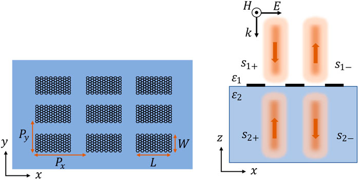
FIGURE 1. Schematic depiction of the graphene cut-wire array. The array is located on a dielectric substrate (left), where the THz wave illuminates the sample perpendicularly either from the air or dielectric side. The polarization of the THz wave is along the x-axis. The periods of the array along the x- and y-axes are denoted as Px and Py, respectively. Parameters L and W delegate the length and width of the cut-wire, respectively. The array can be fabricated by e-beaming lithography (Guo et al., 2018) or standard optical lithography followed by oxygen plasma etching process (Ju et al., 2011).
By solving the differential. Eqs. 1–3, one can obtain,
When the THz wave is illuminated from the air side, i.e.,
Consequently, the total absorption of the GCWA is given by,
The absorption rate of the graphene array is determined by electron scattering rates, impurity and defect densities, which can be approximated as a constant.(Jablan et al., 2009). Therefore, the maximum absorption of the GCWA can be achieved at the condition of
In the QCMT model, ω0, Γrad, and Γabs are phenomenological parameters that are associated with a specific structure. For the GCWA, we can deduce their explicit expressions based on quasistatic PWFs. (Garcıía de Abajo, 2013; Silveiro et al., 2015; Yu et al., 2017). Specifically, in the long-wave limit (q << kF, kF is Fermi wave vector) and high doping condition (EF >>
where e is the charge of an electron,
where
where
For coupled-mode with narrow linewidth (high quality factor Q) and when ω ≈ ω0, Eq. 9 is reduced to the same form as Eq. 5 except a universal phase factor. Therefore, Eqs. 10–12 are explicit expressions of the phenomenological parameters used in QCMT model, which can be applied to calculate the THz wave absorption of the GCWAs.
Several observations can be made from Eqs. 10–12. First, according to Eq. 10, the first term inside the square root represents the oscillation frequency of the individual graphene cut-wire, while the second term is accounted for interactions between different cut-wires in the array. Therefore, when the period of the lattice decreases, plasmon frequency undergoes a small redshift due to such interactions. Second, the absorption rate of GCWA keeps constant as Γabs = τ−1, which is independent of the specific geometry and frequency. This is a direct consequence of electrostatic approximation. Third, the radiative decay rate Γrad is proportional to EF, the duty ratio of the array
Eq. 13 is the central result of this work. That is, with substrate refractive index
We then carried out FEM simulations (COMSOL MULTIPHYSIC)1 to validate the theoretical predictions. To that end, we first verify the critical coupling condition by modeling the optical response of GCWA with different duty ratios (ξ) suspended in the air (nair = 1) and supported onto SiO2 substrate (

TABLE 1. Geometrical parameters for GCWA associated with Figure 1.
The simulated reflection |r|2, transmission |t|2 and absorption A spectra of the two GCWAs are plotted in Figure 2A–C and Figures 2E–G. It can be seen clearly that |r|2, |t|2, and A are strongly dependent on the ξ of the GCWAs. In particular, there exists optimized ξ for the THz absorption of the GCWAs. This can be seen more clearly by plotting the evolution of A at the oscillation frequency of the GCWA as a function of the corresponding ξ (Figures 2D,H, orange squares and lines). Specifically, maximum A can be obtained at ξ = 0.26 and 0.38 for GCWA suspended in the air and supported onto SiO2 substrate, respectively. The two ξ values for optimum absorption condition are exactly the same as those calculated using Eq. 13, where
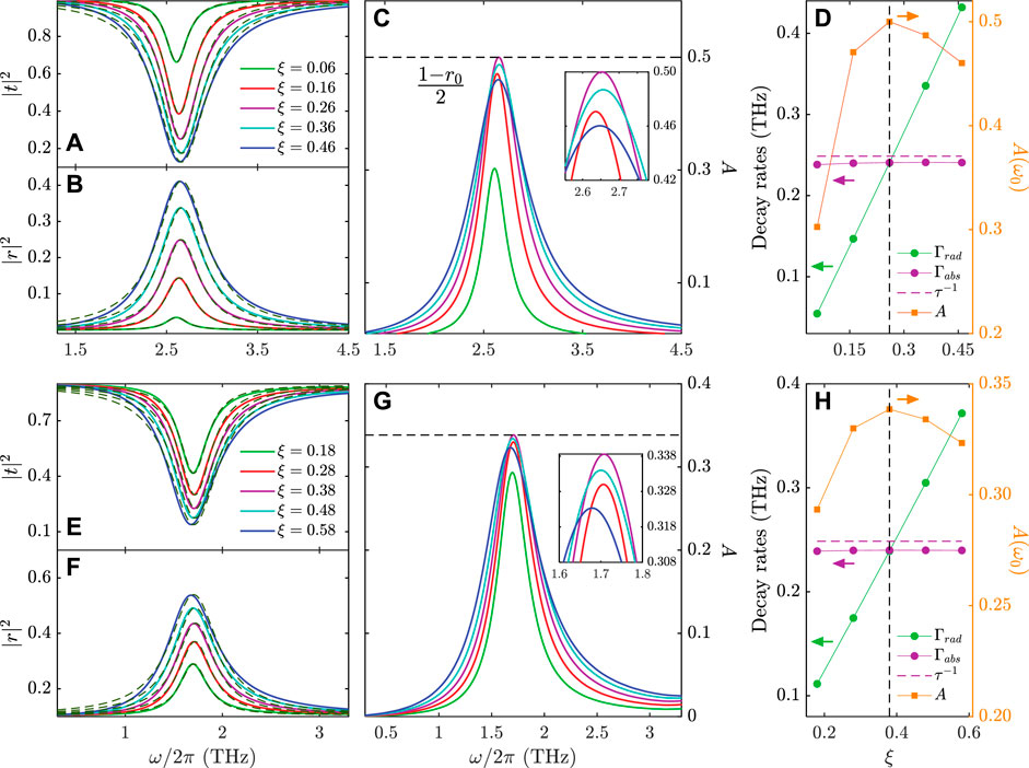
FIGURE 2. THz wave responses of GCWA with different duty ratios. (A–C) Numerical simulations of transmission (A), reflection (B), and absorption (C) spectra for GCWA suspended in the air. (E–G) The corresponding transmission (E), reflection (F), and absorption (G) spectra for GCWA supported onto SiO2 substrate. The gray dashed curves are fittings using the QCMT model. The dashed lines in (C) and (G) are the theoretical maximum absorption calculated by Amax = (1−r0)/2. The insets in (C) and (G) display the magnified absorption spectra near the oscillation frequencies. (D, H) Radiative decay rate Γrad and absorption decay rate Γabs of GCWA suspended in the air (G) and supported onto SiO2 substrate (H). The decay rates are obtained from fitting the spectra shown in Figure (A, B) and (E, F) using the QCMT model. Absorption maxima, A (ω0), extracted at different oscillation frequencies are also included. Dashed black lines shown in (D) and (H) indicate the critical coupling condition.
To further compare the simulation and QCMT model results quantitatively, Eq. 5 obtained from the QCMT model were then employed to fit the simulated spectra. As shown by the dashed lines corresponding to each
We proceed to validate the analytical expressions of ω0 and Γrad (Equation (10) and (11)). These two parameters can be calculated based on the mode eigenvalue η1 and dipole moment ζ1. For graphene cut-wires, they are only determined by the aspect ratio defined as κ = L/W. We first calculated η1 and ζ1 associated with different κ through mode analysis on an isolated graphene cut-wire (more details on the calculations of η1 and ζ1 can be found in Supporting Information, Note 1). As shown in Figure 3A and 3D, η1 decreases against κ, while ζ1 first increases as κ increases and then keeps approximately constant when κ is larger than 1. Because the plasmonic mode is associated with electron oscillations along the x-axis, it becomes a longitudinal mode when κ > 1. Therefore, the dependence of ζ1 on κ indicates that the effective dipole moment of the longitudinal dipole mode of the cut-wire stays unchanged. With the knowledge of η1 and ζ1, we then calculated Γrad and ω0 using Eqations (10) and (11). Different GCWAs with L and W ranging from 5 to 15 μm and 2–8 μm, respectively, are considered. The lattice period is fixed as Px = Py = 24.5 μm. As shown in Figure 3B, Γrad increases as either L or W becomes larger. This is reasonable because the area of the cut-wire D2 is equal to L×W. A larger D2 means that more electrons will be driven by the external field, and consequently more energy will be radiated back to the vacuum due to the stronger electron oscillations. The dependence of working frequency ω0 on the geometrical parameters is shown in Figure 3E. Clearly, when fixing L (W) while increasing W (L), the ω0 increases (decreases) monotonically.
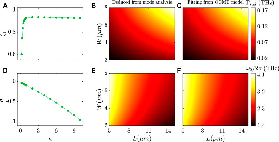
FIGURE 3. Validations of Γrad and ω0 calculated from the QCMT model. (A,D) ζ1 (A) and η1 (D) obtained from mode analysis. The green solid lines are guides for eyes (B,C) Γrad as a function of L and W calculated from Eq. 11 (B) and fitted from QCMT model (C). (E,F) ω0 as a function of L and W calculated from Eq. 10 (E) and fitted from QCMT model (F).
We further simulated the reflection and transmission spectra of the GCWAs with different L and W using the FEM. QCMT model (Equation (5) and (6)) was then employed to fit the simulated spectra and extract the corresponding Γrad and ω0 (Detailed simulations and fitting results can be found in Supporting Information, Note two and Supplementary Figure S1). As shown in Figures 3C,F, the Γrad and ω0 obtained from the QCMT model agree well with those deduced from Eqations (10) and (11), which unambiguously confirms the accuracy of the QCMT model we developed.
It should be emphasized that for graphene cut-wires of mico-meter scale characteristic sizes, our QCMT model and the duty ratio-oriented design can in principle cover a vast geometric space and spectral region ranging from the mid-infrared to THz frequencies, as long as the electrostatic limit is still valid. Specifically, given a dielectric substrate of refractive index ndie and a targeting ω0, the geometrical parameters of GCWA with maximum absorption can be obtained by using Eqs 10–13 and the numerical results shown in Figures 3A,D. To simplify the discussion, we set ζ1 = 0.925 according to Figure 3A, and consequently Eq. 13 can be simplified as,
where α = 80.13 is a dimensionless coefficient. To validate Eq. 14, we consider GCWA with EF = 0.5 eV,
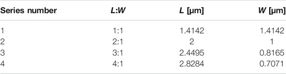
TABLE 2. Geometrical parameters for GCWA associated with Figure 4A.
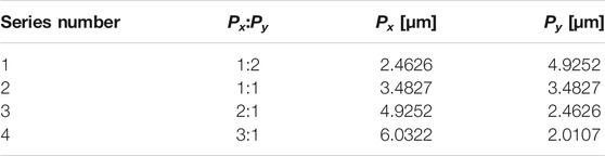
TABLE 3. Geometrical parameters for GCWA associated with Figure 4B.
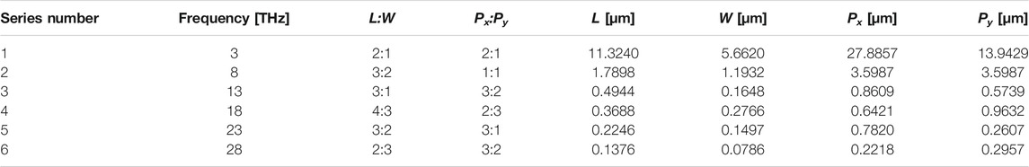
TABLE 4. Geometrical parameters for GCWA associated with Figure 4C.
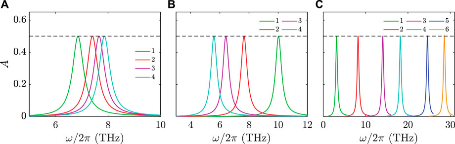
FIGURE 4. Absorption spectra of GCWA with same duty ratio but different geometric parameters. (A) Absorption spectra for GCWAs with the same Px (4.93 μm) and Py (2.46 μm) but different L and W. (B) Absorption spectra for GCWAs with the same L (2 μm) and W (1 μm) but different Px and Py. (C) Absorption spectra for GCWA with different Px, Py, L and W oscillating at 3–28 THz. The duty ratio of GCWAs is fixed to
The analyses in Figures 2–4 have validated the accuracy of our developed QCMT model. This model can be employed as an effective tool to design GCWAs with optimized electromagnetic wave absorption. To demonstrate the capability of the QCMT model, we employed it to design three types of GCWAs with optimum electromagnetic wave absorptions. We consider three types of GCWAs: I) EF = 0.4 eV, ω0 = 30 THz, ndie = 1; II) EF = 0.7 eV, ω0 = 6 THz, ndie = 1.955; III) EF = 1 eV, ω0 = 2 THz, ndie = 3.42. The GCWAs I to III are supported in the air, onto SiO2, and silicon substrates, respectively. In addition, we set the aspect ratios κ of all the three GCWAs to 2. Based on Equations (10) and (11), it is able to deduce the feature size of an individual graphene cut-wire to be L×W = 0.088 μm × 0.044 μm (Type I), 1.63 μm × 0.81 μm (Type II), and 7.92 μm × 3.96 μm (Type III), respectively. According to Eq. 14 the duty ratio of each GCWA can be determined as ξ = 0.2, 0.17, and 0.18, respectively. Afterwards the periods
To validate the above designs, we numerically simulated the absorption spectra of the three types of GCWAs with different duty ratios. The GCWAs are respectively suspended in the air or supported onto SiO2 and silicon substrates. The lengths and widths of the three types of GCWAs are employed according to the QCMT designs. As shown in Figure 5A, for the GCWA suspended in the air (Type I), a working frequency at 31.3 THz (mid-infrared regime) can be found with a duty ratio of 0.2. Additionally, such a duty ratio leads to a maximum peak absorption of 0.5, which is consistent with the QCMT calculation and previous study (Fan et al., 2015). For the GCWAs supported onto SiO2 (Type II) and silicon (Type III) substrates, the maximum absorption occurs for duty ratios of 0.17 and 0.18, respectively (Figures 5B,C). The corresponding working frequencies are 6.23 THz and 2.02 THz, respectively. These results are all corroborated with the QCMT predictions, except for small deviations on the oscillation frequencies (the discrepancies are 4.3% for Type I, 3.8% for Type II and 1% for Type III). We attribute such discrepancies to the deviation of GCWA from quasistatic limitation as well as the high-Q approximation when reducing Equation (9) to Equation (5). Nevertheless, our results unambiguously demonstrate the effectiveness of the QCMT model in designing of GCWAs with optimum electromagnetic absorption in mid-infrared to THz spectral regime.
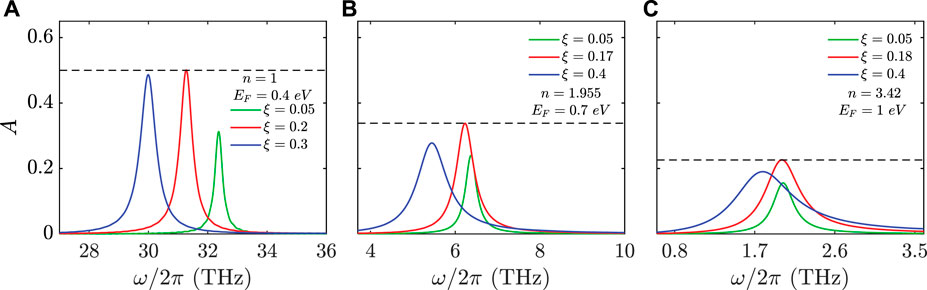
FIGURE 5. Simulated absorption spectra of the GCWAs designed by the QCMT model. The geometrical parameter for each GCWA is: (A) L = 0.088 μm, W = 0.044 μm; (B) L = 1.63 μm, W = 0.81 μm; (C) L = 7.92 μm, W = 3.96 μm. The GCWAs corresponding to (A–C) are respectively suspended in the air (A) and supported onto SiO2 (B) and silicon (C) substrates. For better demonstration, for each array the absorption spectra corresponding to duty ratios that are not associated with the optimum absorption are included. Black dashed lines shown in (A–C) indicate the maximum absorption of each array.
Conclusion
In summary, we have developed an analytical model, i.e., the QCMT model, for designing GCWA with optimum electromagnetic wave absorption in the mid-infrared to THz spectral regime. In the QCMT model, all of the phenomenological parameters employed to calculate the electromagnetic wave reflection and transmission of a specific GCWA can be calculated analytically, which on one hand provides an intuitive physical insight on these parameters, and on the other hand can help optimize the electromagnetic wave absorption of the GCWA. As a result, by utilizing the QCMT model it is able to facilely obtain the geometrical parameters associated with maximum electromagnetic absorption of the GCWA, which otherwise requires arduous parameter securitizing by numerical simulations. We show that a maximum THz wave absorption can be achieved by choosing proper duty ratio of the GCWA, regardless of its working frequencies and other geometrical parameters. The model developed in our study can in principle generalized to other types of polaritonic 2D crystals, which therefore provide a guideline for the design of 2D micro-/nanostructure arrays operating in the long-wave regime with optimized electromagnetic wave absorption.
Data Availability Statement
The original contributions presented in the study are included in the article/Supplementary Material, further inquiries can be directed to the corresponding authors.
Author Contributions
SD, ZC, and HC, conceived and supervised the study. HZ and ZC developed the analytical model and conducted the numerical simulations. The manuscript was written through contributions of all authors. All authors have given approval to the final version of the manuscript.
Funding
This work was financially supported by the National Key Basic Research Program of China (Grant Nos. 2019YFA0210203), the National Natural Science Foundation of China (Grant Nos. 91963205, 11904420, 61905290), and the Guangdong Basic and Applied Basic Research Foundation (Grant Nos. 2020A1515011329, 2019A1515011355, 202102020579). HC acknowledges the support from Changjiang Young Scholar Program. SD, ZC, and HC conceived and supervised the study. HZ, and ZC developed the analytical model and conducted the numerical simulations. The manuscript was written through contributions of all authors. All authors have given approval to the final version of the manuscript.
Conflict of Interest
The authors declare that the research was conducted in the absence of any commercial or financial relationships that could be construed as a potential conflict of interest.
Publisher’s Note
All claims expressed in this article are solely those of the authors and do not necessarily represent those of their affiliated organizations, or those of the publisher, the editors and the reviewers. Any product that may be evaluated in this article, or claim that may be made by its manufacturer, is not guaranteed or endorsed by the publisher.
Supplementary Material
The Supplementary Material for this article can be found online at: https://www.frontiersin.org/articles/10.3389/fmats.2021.737347/full#supplementary-material
Footnotes
1https://www.comsol.com/, accessed.
References
Abd El-Fattah, Z. M., Mkhitaryan, V., Brede, J., Fernández, L., Li, C., Guo, Q., et al. (2019). Plasmonics in Atomically Thin Crystalline Silver Films. ACS Nano 13, 7771–7779. doi:10.1021/acsnano.9b01651
Atwater, H. A., and Polman, A. (2010). Plasmonics for Improved Photovoltaic Devices. Nat. Mater 9, 205–213. doi:10.1038/nmat2629
Basov, D. N., Fogler, M. M., and García de Abajo, F. J. (2016). Polaritons in van der Waals materials. Science 354, aag1992. doi:10.1126/science.aag1992
Cui, L., Wang, J., and Sun, M. (2021). Graphene Plasmon for Optoelectronics. Rev. Phys. 6, 100054. doi:10.1016/j.revip.2021.100054
Fan, S., Suh, W., and Joannopoulos, J. D. (2003). Temporal Coupled-Mode Theory for the Fano Resonance in Optical Resonators. J. Opt. Soc. Am. A. 20, 569. doi:10.1364/josaa.20.000569
Fan, Y., Shen, N.-H., Koschny, T., and Soukoulis, C. M. (2015). Tunable Terahertz Meta-Surface with Graphene Cut-Wires. ACS Photon. 2, 151–156. doi:10.1021/ph500366z
Fan, Y., Wei, Z., Zhang, Z., and Li, H. (2013). Enhancing Infrared Extinction and Absorption in a Monolayer Graphene Sheet by Harvesting the Electric Dipolar Mode of Split Ring Resonators. Opt. Lett. 38, 5410. doi:10.1364/ol.38.005410
Fang, Z., Thongrattanasiri, S., Schlather, A., Liu, Z., Ma, L., Wang, Y., et al. (2013). Gated Tunability and Hybridization of Localized Plasmons in Nanostructured Graphene. ACS Nano 7, 2388–2395. doi:10.1021/nn3055835
García de Abajo, F. J. (2007). Colloquium: Light Scattering by Particle and Hole Arrays. Rev. Mod. Phys. 79, 1267–1290. doi:10.1103/revmodphys.79.1267
García de Abajo, F. J. (2014). Graphene Plasmonics: Challenges and Opportunities. ACS Photon. 1, 135–152. doi:10.1021/ph400147y
Garcıía de Abajo, F. J. (2013). Multiple Excitation of Confined Graphene Plasmons by Single Free Electrons. ACS Nano 7, 11409. doi:10.1021/nn405367e
Gramotnev, D. K., and Bozhevolnyi, S. I. (2010). Plasmonics beyond the Diffraction Limit. Nat. Photon 4, 83–91. doi:10.1038/nphoton.2009.282
Guo, C., Zhang, J., Xu, W., Liu, K., Yuan, X., Qin, S., et al. (2018). Graphene-Based Perfect Absorption Structures in the Visible to Terahertz Band and Their Optoelectronics Applications. Nanomaterials 8, 1033. doi:10.3390/nano8121033
Guo, Q., Yu, R., Li, C., Yuan, S., Deng, B., García de Abajo, F. J., et al. (2018). Efficient Electrical Detection of Mid-infrared Graphene Plasmons at Room Temperature. Nat. Mater 17, 986–992. doi:10.1038/s41563-018-0157-7
Hanson, G. W. (2008). Dyadic Green's Functions and Guided Surface Waves for a Surface Conductivity Model of Graphene. J. Appl. Phys. 103, 064302. doi:10.1063/1.2891452
Huard, B., Sulpizio, J. A., Stander, N., Todd, K., Yang, B., and Goldhaber-Gordon, D. (2007). Transport Measurements across a Tunable Potential Barrier in Graphene. Phys. Rev. Lett. 98, 236803. doi:10.1103/physrevlett.98.236803
Jablan, M., Buljan, H., and Soljačić, M. (2009). Plasmonics in Graphene at Infrared Frequencies. Phys. Rev. B 80, 245435. doi:10.1103/physrevb.80.245435
Ju, L., Geng, B., Horng, J., Girit, C., Martin, M., Hao, Z., et al. (2011). Graphene Plasmonics for Tunable Terahertz Metamaterials. Nat. Nanotech 6, 630–634. doi:10.1038/nnano.2011.146
Kabashin, A. V., Evans, P., Pastkovsky, S., Hendren, W., Wurtz, G. A., Atkinson, R., et al. (2009). Plasmonic Nanorod Metamaterials for Biosensing. Nat. Mater 8, 867–871. doi:10.1038/nmat2546
Liu, P., Cai, W., Wang, L., Zhang, X., and Xu, J. (2012). Tunable Terahertz Optical Antennas Based on Graphene Ring Structures. Appl. Phys. Lett. 100, 153111. doi:10.1063/1.3702819
Low, T., and Avouris, P. (2014). Graphene Plasmonics for Terahertz to Mid-infrared Applications. ACS Nano 8, 1086–1101. doi:10.1021/nn406627u
Luk'yanchuk, B., Zheludev, N. I., Maier, S. A., Halas, N. J., Nordlander, P., Giessen, H., et al. (2010). The Fano Resonance in Plasmonic Nanostructures and Metamaterials. Nat. Mater 9, 707–715. doi:10.1038/nmat2810
Luo, X., Qiu, T., Lu, W., and Ni, Z. (2013). Plasmons in Graphene: Recent Progress and Applications. Mater. Sci. Eng. R: Rep. 74, 351–376. doi:10.1016/j.mser.2013.09.001
Maier, S. A. (2007). Plasmonics: Fundamentals and Applications. Berlin, Germany: Springer Science & Business Media.
Novotny, L., and van Hulst, N. (2011). Antennas for Light. Nat. Photon 5, 83–90. doi:10.1038/nphoton.2010.237
Otsuji, T., Popov, V., and Ryzhii, V. (2014). Active Graphene Plasmonics for Terahertz Device Applications. J. Phys. D: Appl. Phys. 47, 094006. doi:10.1088/0022-3727/47/9/094006
Schuller, J. A., Barnard, E. S., Cai, W., Jun, Y. C., White, J. S., and Brongersma, M. L. (2010). Plasmonics for Extreme Light Concentration and Manipulation. Nat. Mater 9, 193–204. doi:10.1038/nmat2630
Shalaev, V. M. (2007). Optical Negative-index Metamaterials. Nat. Photon 1, 41–48. doi:10.1038/nphoton.2006.49
Shen, N.-H., Tassin, P., Koschny, T., and Soukoulis, C. M. (2014). Comparison of Gold- and Graphene-Based Resonant Nanostructures for Terahertz Metamaterials and an Ultrathin Graphene-Based Modulator. Phys. Rev. B 90, 115437. doi:10.1103/physrevb.90.115437
Silveiro, I., Ortega, J. M. P., and Abajo, F. J. G. d. (2015). Plasmon Wave Function of Graphene Nanoribbons. New J. Phys. 17, 083013. doi:10.1088/1367-2630/17/8/083013
Thongrattanasiri, S., Koppens, F. H. L., and García de Abajo, F. J. (2012). Phys. Rev. Lett. 108, 047401. doi:10.1103/physrevlett.108.047401
Wang, W. (2012). Plasmons and Optical Excitations in Graphene Rings. J. Phys. Condens. Matter 24, 402202. doi:10.1088/0953-8984/24/40/402202
Xu, H., Bjerneld, E. J., Käll, M., and Börjesson, L. (1999). Spectroscopy of Single Hemoglobin Molecules by Surface Enhanced Raman Scattering. Phys. Rev. Lett. 83, 4357–4360. doi:10.1103/physrevlett.83.4357
Yan, H., Li, X., Chandra, B., Tulevski, G., Wu, Y., Freitag, M., et al. (2012). Tunable Infrared Plasmonic Devices Using Graphene/insulator Stacks. Nat. Nanotech 7, 330–334. doi:10.1038/nnano.2012.59
Keywords: graphene, terahertz, plasmons, absorption enhancements, coupled-mode theory, arrays
Citation: Zhu H, Wang X, Cao Z, Chen H and Deng S (2021) A Universal Approach for Maximizing Terahertz Wave Absorption in Graphene Cut-Wires. Front. Mater. 8:737347. doi: 10.3389/fmats.2021.737347
Received: 06 July 2021; Accepted: 02 August 2021;
Published: 16 August 2021.
Edited by:
Umberto De Giovannini, Max-Planck-Gesellschaft (MPG), GermanyCopyright © 2021 Zhu, Wang, Cao, Chen and Deng. This is an open-access article distributed under the terms of the Creative Commons Attribution License (CC BY). The use, distribution or reproduction in other forums is permitted, provided the original author(s) and the copyright owner(s) are credited and that the original publication in this journal is cited, in accordance with accepted academic practice. No use, distribution or reproduction is permitted which does not comply with these terms.
*Correspondence: Zhaolong Cao, Y2Fvemhsb25nQG1haWwuc3lzdS5lZHUuY24=; Shaozhi Deng, c3RzZHN6QG1haWwuc3lzdS5lZHUuY24=