 G. L. Kabongo
 B. M. Mothudi
- Department of Physics, CSET, University of South Africa, Pretoria, South Africa
Energy is the driving force behind the upcoming industrial revolution, characterized by connected devices and objects that will be perpetually supplied with energy. Moreover, the global massive energy consumption increase requires appropriate measures, such as the development of novel and improved renewable energy technologies for connecting remote areas to the grid. Considering the current prominent market share of unsustainable energy generation sources, inexhaustible and clean solar energy resources offer tremendous opportunities that, if optimally exploited, might considerably help to lessen the ever-growing pressure experienced on the grid nowadays. The R&D drive to develop and produce socio-economically viable solar cell technologies is currently realigning itself to manufacture advanced thin films deposition techniques for Photovoltaic solar cells. Typically, the quest for the wide space needed to deploy PV systems has driven scientists to design multifunctional nanostructured materials for semitransparent solar cells (STSCs) technologies that can fit in available household environmental and architectural spaces. Specifically, Plasma Enhanced Chemical Vapor Deposition (PECVD) technique demonstrated the ability to produce highly transparent coatings with the desired charge carrier mobility. The aim of the present article is to review the latest semi-transparent PV technologies that were impactful during the past decade with special emphasis on PECVD-related technologies. We finally draw some key recommendations for further technological improvements and sustainability.
Introduction
In recent decades, thousands of research reports related to green renewable energy have attracted the attention of scientists worldwide. One of the inexhaustible energy generation sources that can successfully suit mankind’s need for sustainable socio-economic growth in an interconnected world is the sun (IEA, 2020; Jacobson et al., 2017; IRENA, 2020; Brinkerink et al., 2018; Kim et al., 2020; Huang and Luscombe, 2019; Burke and Lipomi, 2013). The direct conversion of sunlight to electricity, well known as photovoltaic energy conversion, has been successfully demonstrated using various photonic materials with high photon absorption capabilities classified in two main categories, organic and inorganic semiconductors (Nakamura et al., 2019; Kim et al., 2020). The successfully converted solar energy is used in daily life activities such as water heating, solar cooking, deep water pumping, household device PV powering, and clean hydrogen generation, out of a total annual provision of 18 TW solar energy available on the earth’s surface (Smyth et al., 2005; Kalyanasundaram and Grätzel, 2012; Chandel et al., 2015; Aramesh et al., 2019; Kuang et al., 2019).
Sunlight to electrical energy conversion without the interference of any intermediary thermal generator leads to photovoltaic (PV) conversion. The PV conversion process takes place in an electron device, known as a solar cell, which is a component from which the power output is the conjunction of mechanical, electrical, and photophysical properties, mainly (Green, 2020). For decades, scientists have been working on the enhancement of key technical characteristics such as efficiency, which is expressed as a fractional relationship of the output generated current over the incoming absorbed photons under specific irradiance conditions (Green, 2020). Interestingly, several approaches were found to considerably enhance the efficiency of PV solar cells; these include intrinsic and extrinsic factors, both related to the thin films’ deposition techniques (Kemell et al., 2005). Generally, thin film solar cell components are fabricated using various vacuum and non-vacuum deposition techniques such as sol-gel spin coating, spray coating, doctor blade, drop casting, dip coating, ink-jet evaporation, Pulsed Laser Deposition, Chemical Vapor Deposition (MOCVD), Molecular Beam Epitaxy (MBE), Electron-Beam Physical Vapor Deposition (EBPVD), magnetron sputtering, and Plasma Enhanced Chemical Vapor Deposition (PECVD) (Steirer et al., 2009; Eslamian, 2014; Eslamian and Zabihi, 2015; Lu et al., 2015; Leyden et al., 2016; Farrag and Balboul, 2017; Matur and Baydogan, 2017; Hodgkinson et al., 2018; Abzieher et al., 2019; Ji et al., 2019; Lim et al., 2021a; Smirnov et al., 2021; Sun et al., 2021).
An extensive survey by solar PV specialists established that there exist three generations of PV solar technology that have been reported so far (Khatibi et al., 2019; Green et al., 2020), among which semi-transparent photovoltaic solar cells (STPSCs) is one of the most promising for the next generation of environmentally friendly renewable energy sources (Lim et al., 2021b). STPSCs have been recently manufactured via thin films’ deposition techniques such as Inkjet printing, Pulsed laser deposition (PLD), and PECVD as reported in recent studies. This includes perovskite solar cells which reached a record high efficiency of over 25% (Cheng et al., 2014; Xie et al., 2018; Corzo et al., 2020; Lim et al., 2021b). In addition, recent studies have demonstrated that the use of various protective and antireflective coatings, such as intrinsic a-Si:H layers, among others, can considerably enhance the performance of future generations of thin film solar cells (Uzum et al., 2017; Zhao et al., 2017; Li et al., 2020a; Bacal et al., 2020; Qu et al., 2021). The scientific community devoted to semitransparent solar cell technology research may consider the recent advent of monolithic Perovskite/Si tandem solar cells as a unique opportunity to reshape the current knowledge in the field, allowing the possibility to reach the Shockley-Queisser theoretical efficiency limit of 33% (Ail-Ashouri et al., 2020; Lu et al., 2020). The present review is mainly devoted to Semi-transparent solar cells technology with special focus on Plasma Enhanced Chemical deposition (PECVD)-based devices.
Background of Building-Integrated Photovoltaics Technology
Building-integrated photovoltaics (BIPVs) are considered as the most promising option that will boost renewable energy among all PVs currently available in the market (IEA et al., 1996). Global reports from well-established renewable energy institutions ascertain that in the entire PV solar technology market, approximately USD 14.4 billion was attributed to BIPVs technology in 2020 (EMR, 2021). Considering that semitransparent solar cells are among the major components in BIPVs, this technology will obviously benefit from the net market growth estimated at about 20% for the next 6 years (see Figure 1A); (EMR, 2021). Prospective actors in the renewable energy sector have to consider two major categories of BIPV technologies depending on their architectural need, namely roof-based and façade-based BIPVs. Moreover, these categories are mainly shared among crystalline silicon and thin films solar technologies (see Figure 1B). Notwithstanding the perceived bright future of BIPV, stakeholders are constantly driven by the predominant circular economy vision of national governments, which are mostly eagerly engaged in the successful greener fourth industrial revolution. In a recent report by the Becquerel Institute, three BIPV products were defined. Among these, glazed semi-transparent BIPV offers flexibility for effective integration in both building roofs and façades (Curti et al., 2020); (see Figure 1C).
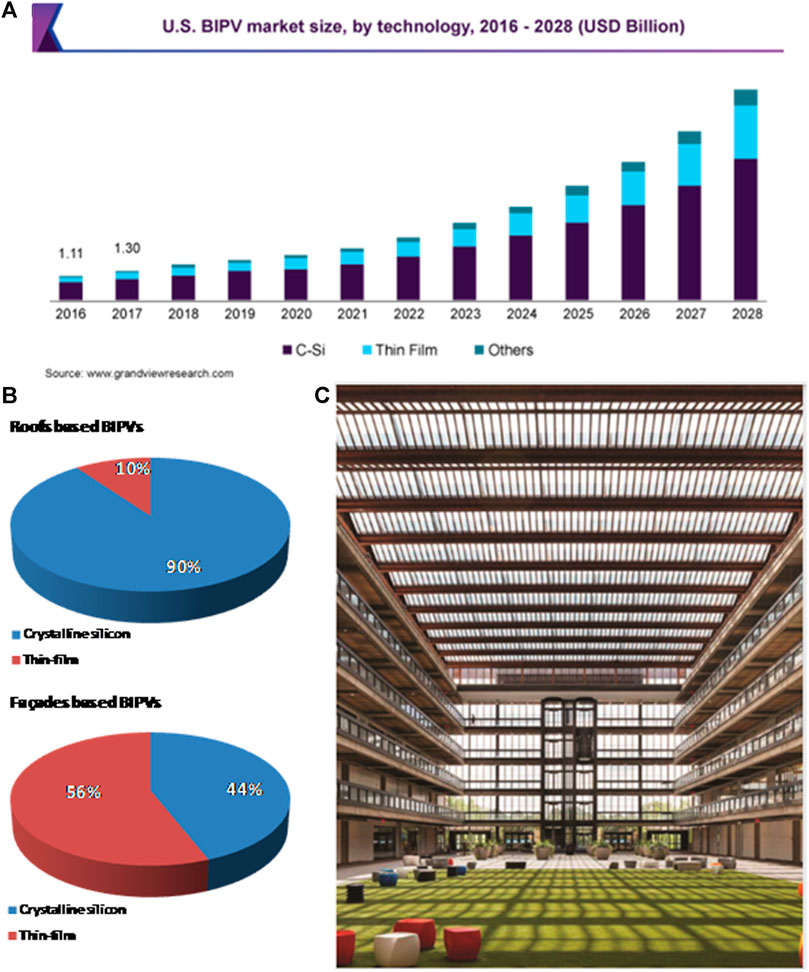
FIGURE 1. (A) US forecast of BIPV market, © (2021) Grand View Research (EMR, 2021). (B) BIPV technologies split for (top) roof and (bottom) façade applications, respectively. Redrawn from (Zanetti et al., 2017). (C) Photograph of semitransparent BIPVs BellWorks, skylight, United States. Reprinted with permission © Onyx Solar (Curti et al., 2020).
PV Cell Working Principle
Put simply, a photovoltaic solar cell is an electron device characterized by three main parts, amongst which the photoactive layer, the electrons and holes transport layers, and the electrical contact layers are deposited on a transparent substrate (Figure 2).
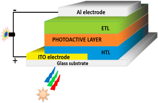
FIGURE 2. Structure of organic PV solar cell device (ETL and HTL denote electron and hole transport layer, respectively).
The photoactive central layer is preferably a direct band gap semiconductor material that is highly sensitive to photon absorption throughout the entire electromagnetic solar spectrum. Moreover, the photoactive layer forms a PN junction with the electron transport layer, similar to a diode where electron-hole pairs ‘‘excitons’’ are generated after photon absorption (Gray et al., 2011). Consecutively, the generated charge carriers are dissociated due to the presence of an electric field at the PN junction as to allow electrons and holes to migrate at the negative and positive electrode terminal, respectively (Figure 3); (Markvart and Castaner, 2003). The resulting direct current flow throughout the device PN junction follows a single direction from the negative to the positive terminal. It is worth mentioning that among factors that affect the PV solar cell efficiency, the diffusion length is the most prominent which requires detailed time resolved fluorescence analysis for better understanding.
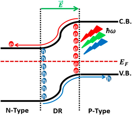
FIGURE 3. Schematic band diagram of a solar cell device as a PN junction.
PECVD Deposition Technique
Background
Plasma Enhanced Chemical Vapor Deposition (PECVD) was first demonstrated in the fifties and sixties at various laboratories. Their research outputs are among the most seminal traceable proofs known to date (Poole, 1953; Ennos, 1954; Christy, 1960; Baker and Morris, 1961; Christy, 1962; Alt et al., 1963; Ing and Davern, 1964). Since its discovery almost 6 decades ago, PECVD has successfully overcome the major drawbacks encountered in the use of other deposition techniques as well as conventional wet chemistry. Moreover, PECVD is one of the main processes used in the nanofabrication of electron devices in order to deposit high quality thin film semiconductors (Jeong et al., 2020). Generally, in nanofabrictation, PECVD of a thin film immediately follows the doping of silicon compound film pre-grown on Si wafer with either Arsenic, phosphorous, or boron via Ion Implantation which aims to tune the conductivity, relative to a particular technology application of the semiconductor industry (Skorupa et al., 1987; Yokota et al., 1994). Consecutively to PECVD process, a lithography process is used to apply a pattern on the thin film semiconductor via a pre-coated photoresist film using either EUV light or electron beam (Desai et al., 2016; Shamma et al., 2016; Van de Kerkhof et al., 2021).
Fundamental Principles
The PECVD thin films deposition technique is a complex process deriving from the conventional chemical vapor deposition (CVD) which can operate either in open or closed reactor configurations, the latter being the most convenient for industrial usage (Martinu et al., 2010). Generally, the operation of CVD systems consists of filling the reaction chamber with reactants via a supply section designed to allow easy delivery of solid, liquid, or gaseous reactants for substrate coating under vacuum (Figure 4). However, due to the drawbacks resulting from solids and liquids reactants management, gaseous reactants are used in PECVD processes in which the reactant is delivered in the reaction chamber via gas-flowing elements, coupled to computer-controlled pressure controllers. The chemical reaction is activated by a low-temperature inductively/capacitively-coupled plasma produced by DC or RF power source, which, in contrast to other CVD techniques, uses the plasma as a source of activation energy instead of high temperatures, allowing much larger flexibility in substrates and samples diversity (Bera et al., 2002). It is worth mentioning that the produced plasma has the characteristics of the “inert” carrier gas, such as Ammonia, Argon, Helium, Nitrogen, and Oxygen, used in the process, including their derived forming gasses. PECVD-deposited thin films’ high quality and superior properties are governed by various parameters including RF power, plasma temperature, reactor pressure, gas phase diffusion, and gas flow rate in addition to the types of carriers and reacting gases. Typically, the neutrally charged and highly energetic plasma used during PECVD thin films deposition is a partially or totally ionized gas composed of charged particles, electrons, and neutral atoms constituents (Hamedani et al., 2016). The main PECVD setups are presented in the next sections.
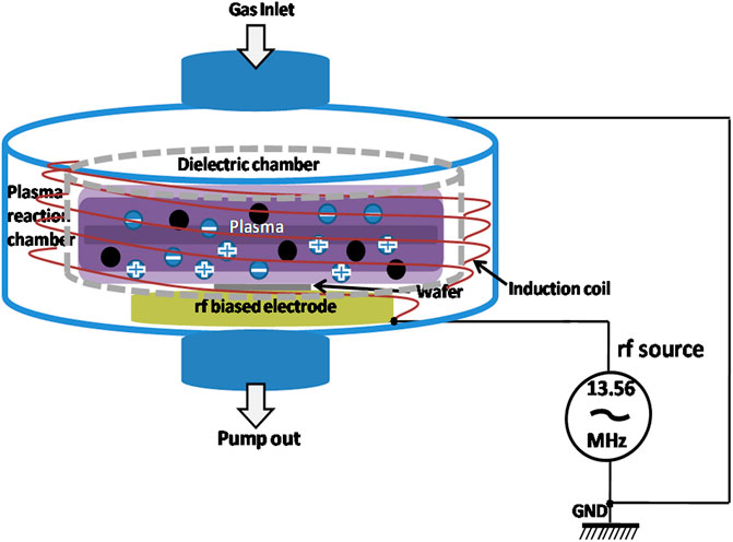
FIGURE 4. Schematic configuration setup of Inductively Coupled Plasma.
Over the years, tremendous advancements have resulted in the development of several plasma technologies to fit scientific research needs. This has led to the identification of two major plasma classifications: thermal and non-thermal plasma. The class of thermal plasma techniques includes inductively coupled plasma (ICP) (Jatta et al., 2019), electron cyclotron resonance chemical vapor deposition (ECR-CVD) (Hu et al., 2015), direct-current plasma (DCP) (Wahyudiono et al., 2020), direct current-inductively coupled (DC-ICP) hybrid (Kambara et al., 2014), and plasma spraying (Navidpour et al., 2017). On the other hand, capacitively coupled plasma (CCP) (Fang et al., 2016), Dielectric barrier discharge (DBD) (Tsai et al., 2020), Glow discharge (GD) (Schmitt et al., 1988), Plasma Enhanced Atomic Layer Deposition (PEALD) (Jin et al., 2013), and DC Magnetron sputtering (Kim et al., 2012) are non-thermal plasma deposition techniques. Despite the progress made in the Plasma technologies, there is still hot debate on the constituent of the deposited film mass because the ions and neutral species present in the plasma behave differently depending on the dynamic physical and chemical conditions (Michelmore et al., 2015).
Inductively Coupled Plasma
In the inductively coupled plasma (ICP) deposition, the ionized gas is obtained by coupling the electromagnetic field produced by a coil within the reaction chamber without the need for paired electrodes (Cuxart et al., 2017). The radiofrequency (RF)-ICP is a thermal plasma system which can perform thin films deposition in a wide variety of environments, such as oxidizing, reducing, inert, and many more reactive atmospheres (Cuxart et al., 2017). It is worth noting that ICP-PECVD configuration allows an extremely high purified environment appropriate for the synthesis of nanomaterials requiring accurate control of morphology and chemistries (Cuxart et al., 2017). The ICP configuration is advantageous as compared to its counterpart due to its higher energy density capabilities; its setup is presented below in Figure 4.
Capacitively Coupled Plasma
In the plasma deposition system industry, most non-thermal radio frequency plasma are generated by capacitively coupling two metal electrodes short-distanced placed in the reaction chamber, one of which is connected to a single frequency microwave RF power source (13.56 MHz) and the other of which is grounded (Ohtsu, 2018). Upon electric field appearance in between the electrodes, atoms are ionized in order to release electrons which are accelerated by the RF electric field to produce secondary electrons leading to electron-avalanche due to the exponential field increase (Ohtsu, 2018). Consecutively, an electron-avalanche breakdown will make the gas electrically conductive due to its large number of bind-free electrons and allow perfect surface coating (Ohtsu, 2018). The schematic principle of CCP, which is similar to a conventional capacitor, is presented in Figure 5.
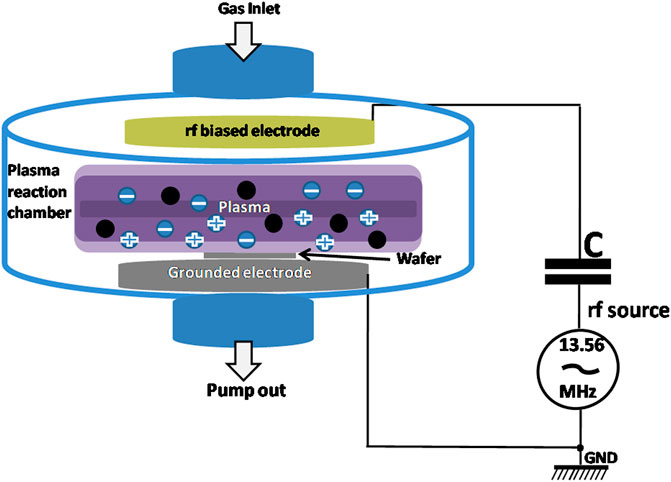
FIGURE 5. Basic schematic principle of Capacitively Coupled Plasma.
Technology Application
PECVD is promising in the entire nanofabrication of semiconductor-based devices (see Figure 6), however, there is still room for improvement when real device commercialization comes in to play. It is worth noticing that notable results such as in Solar cells (Gabriel et al., 2014), Light emitting diodes (LEDs) display (Park et al., 2019), Sensors (Forleo et al., 2009), photocatalysis (Nada et al., 2017), triboelectric nanogenerators (TNGs) (Wang et al., 2016), Thin Film Transistors (TFTs) (Park et al., 2008), non-Volatile Memories (NVMs) (Choi et al., 2007), integrated circuits (Zhang et al., 2013), neutron detection (Bute et al., 2021), diamond growth (Mankelevich and May 2008), photonic waveguides (Neutens et al., 2019), energy storage (Quesnel et al., 2016), and UV photodetectors (Chao and Wei, 2015) are essential to the successful development of the next generation of commercially viable electronic devices.
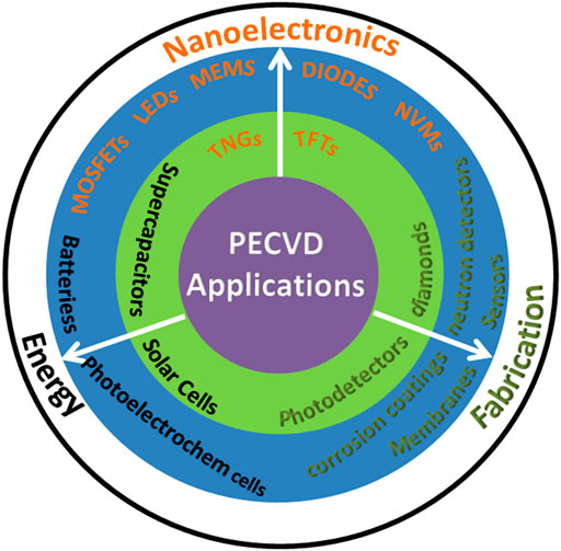
FIGURE 6. Various applications of PECVD.
Semitransparent PECVD Solar Technology
The concept of semitransparent electron devices dates back to the early 2000s when Forrest’s group first successfully demonstrated semitransparent cathodes for organic light emitting devices prior to its solar cells application 6 years later (Burrows et al., 2000; Bailey-Salzman et al., 2006). Moreover, the promise of the concept was successfully followed by the so-called inverted solar cell configuration which was initially applied to organic photovoltaic solar cells (OPVSCs) in Yang’s group (Li et al., 2006). In his seminal work on semitransparent OPVSCs, Bailey-Salzman et al. (Bailey-Salzman et al., 2006) astoundingly envisioned the use of multiple paints in the form of thin films coated on building walls and windows to generate power (Chae et al., 2014). Fifteen years later, tremendous progress (see table 1) was made on the use of this architectural-friendly concept which has been successfully integrated in other solar cell technologies, among which the most prominent based on PECVD are discussed in the following subsections.
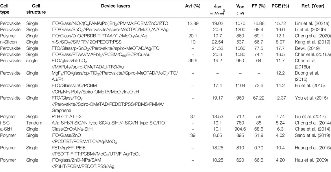
TABLE 1. Summary performances of the representative semitransparent PV solar cells.
Silicon Solar Cells
Recently, a group of scientists developed a semitransparent non-stoichiometric photovoltaic solar cell based on Si-rich SixC1-x p-i-n grown by hydrogen-free PECVD at low plasma power (Cheng et al., 2014). During the fabrication process using RF plasma power ranging from 20–100 W (40W step) at a power density of 560 mW cm−2, the optical bandgap of Si-rich SixC1-x absorbing layer was effectively controlled by varying the Si/C ratio. Moreover, the device absorbing layer was sandwiched in between a SixC1-x:P and SixC1-x:B which were doped at various fluences to accurately define their conductivity for ensuring optimal charge mobility across the device. Furthermore, the charge collection process was realized using ITO and Al electrode which were connected to P-type SiC and N-type SiC films respectively (see Figure 7). Ultimately, the optimized device fabricated with an absorbing layer of 25 nm exhibited the highest power conversion efficiency (Cheng et al., 2014). The optimization of deposition parameters remains a key challenge for better performance of the devices (see table 2).
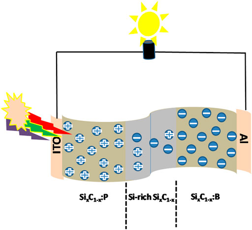
FIGURE 7. Schematic drawing of the device structure.
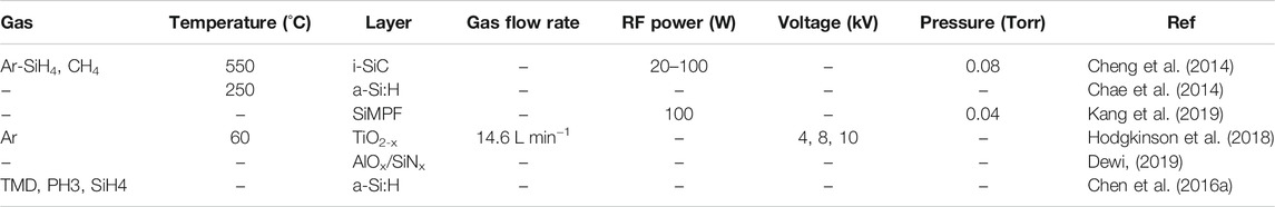
TABLE 2. Summary of PECVD parameters used in semitransparent PV solar cells thin films’ growth.
In 2014, Chae and colleagues (Chae et al., 2014) successfully integrated semitransparent solar cells in building windows via building integrated photovoltaic (BIPV). In the study, two parameters were considered to evaluate the performance of the devices: the thickness of a-Si:H absorbing layer and the applied texture. The p-i-n absorbing layer was deposited via PECVD at 250°C on glass substrate pre-coated with ZnO:Al film. Moreover, the tuning of parameters revealed enhanced power conversion efficiency (PCE) in the device with 180 nm thicker absorbing layer, the performance of which was further improved with texturing to reach 6.3% PCE.
Elsewhere, Kang et al. (Kang et al., 2019) applied engineering light absorption to fabricate a transparent solar cell with a 70 nm thick SiN AR coating deposited via PECVD on the SiMW tips. The resulting JSC considerably increased from 17.07 to 18.94 mA cm−2 while the other key parameters did not undergo the expected changes due to the decrease of VOC and ideality factor FF relative to the device without SiN AR layer. The authors attributed the VOC decrease to the localization of the n-Si and p-PEDOT heterojunctions which formed only on the side surface and not on the top surface of SiMWs, resulting in hampering electron-hole pairs’ generation.
Perovskite Solar Cells
Nowadays, perovskite solar cells are recording unprecedented momentum across the scientific community worldwide due to their versatile properties and easy and sustainable processing (Leyden et al., 2016; Jain et al., 2019; Tavakoli et al., 2019; Zhu et al., 2019; Elseman et al., 2020a; Asuo et al., 2020; Elseman et al., 2020b; Rahmany and Etgar, 2020; Selim and ElsemanHao, 2020; Xu et al., 2020; Chen et al., 2021; Cui et al., 2021; Heshmati et al., 2021; Jeong et al., 2021; Tong et al., 2021). In 2018, a research group innovatively demonstrated that the application of atmospheric pressure plasma enhanced chemical vapor deposition (AP PECVD) can contribute to improving the efficiency of a perovskite solar cell. Technically, the roll-to-roll plasma system used Argon gas flow and an audio frequency power supply (3.4 kHz) which activated the plasma under a potential of 4 and 8 kV to achieve 10.68 m hr−1 line speed for the deposition of mesoporous TiO2 film (Hodgkinson et al., 2018). The deposited film served as the hole blocking layer coated on top of the TCO of the solar cell; afterward, the performance of the device was compared to a reference cell with the TiO2-x electron transport layer sputtered using an RF source at 60ºC in argon along with oxygen at a pressure of 7.5 x 10⁻⁶ mbar (Hodgkinson et al., 2018). It is worth mentioning that this strategy consisting in the tuning of the electronic properties of the Electron transport layer and/or hole transport layer was found to be beneficial in the decline of their parasitic absorption (Li et al., 2020b).
In a completely different study, the optimized use of Aluminum-doped ZnO (AZO) as a transparent electrode (TE) of a semitransparent perovskite solar cell (ST-PSCs) in a tandem perovskite/Si device contributed to reaching power conversion efficiency (PCE) of 23.1% (Li et al., 2020b). The authors particularly stressed the crucial role of the transparency and conductivity of the TE in the high performance of ST-PSCs which constituted the top part of the tandem device. Interestingly, the AZO layer was found to bring more stability in the device relative to devices without an AZO layer (Li et al., 2020b). Moreover, in this tandem solar cell device, the PECVD technique was successfully used to deposit the lower silicon bi-layer TOPCon structure, including the hydrogenated silicon nitride (SiNx:H) which served as anti-reflection coating and front passivation layer. Finally, the tandem semitransparent concept demonstrated to perform better with PCE reaching over 20% (Chen et al., 2016a; Dewi, 2019).
Concluding Remarks and Future Prospects
The present review highlighted the recent advances in the development of semitransparent solar cells, which offers a promising future in building integrated photovoltaic applications. The review shows that the emergence of semitransparent solar cell technologies is mainly driven by research undertaken in polymer solar cells, perovskite solar cells, and Si-based solar cells. To be more concise, we focused our effort on semitransparent technologies that used the versatile advantages offered by PECVD technique owing to its applicability in matured industrial manufacturing processes. We surprisingly realized that, despite the unique strengths of PECVD thin film deposition, very limited numbers of reports on semitransparent solar cells are available to date. Nonetheless, PECVD demonstrated its efficacy in several semitransparent solar cells including monolithic perovskite/Si tandem solar cells, which are currently exhibiting the highest power conversion efficiency in the entire field.
Considering factors that hamper the optimal performance of semitransparent solar cells, mainly polymers and perovskites-based PV, some recommendations are necessary to contribute to improving the manufacturing processes of future generations of semitransparent solar cells:
1) Encapsulation of the device using a thin dielectric layer with higher resistance to UV degradation and thermal oxidation in addition to a good light transmission aiming to combat oxygen infiltration and moisture. Particular care will be required to ensure that the encapsulating layer exhibits higher oxygen transmission rate (OTR) and water vapor transmission (WPTR), which are governed by Fick’s law (Uddin et al., 2019).
2) Reinforced PECVD is one of the most adapted solutions to perform encapsulation at low temperatures. However, stringent precautions are recommended, especially the passivation of intrinsic defects which persist to single layer encapsulation.
Looking ahead, great effort is still required to innovatively design and fabricate industrially viable high quality and colorless semitransparent photovoltaic solar cells that meet the requirement for building and window integration. This includes the stringent control of PECVD parameters/factors such as gas flow rate, pressure, voltage, gas mixture, rf power, platen temperature, and plasma chemistry during the formation of the various layers and the application of tunnel oxide passivating contacts (Yoon et al., 2020).
Author Contributions
GK: Data acquisition, investigation, analysis, writing-original draft manuscript; MD: Supervision, resources, project administration, writing-draft review, funding acquisition. BM: supervision, administration and technical support.
Funding
The present research was funded by the University of South Africa.
Conflict of Interest
The authors declare that the research was conducted in the absence of any commercial or financial relationships that could be construed as a potential conflict of interest.
Publisher’s Note
All claims expressed in this article are solely those of the authors and do not necessarily represent those of their affiliated organizations, or those of the publisher, the editors and the reviewers. Any product that may be evaluated in this article, or claim that may be made by its manufacturer, is not guaranteed or endorsed by the publisher.
References
Abzieher, T., Moghadamzadeh, S., Schackmar, F., Eggers, H., Sutterluti, F., Farooq, A., et al. (2019). Electron-Beam-Evaporated Nickel Oxide Hole Transport Layers for Perovskite-Based Photovoltaics. Adv. Energ. Mater. 9 (120), 1802995. doi:10.1002/aenm.201802995
Ail-Ashouri, A., Köhnen, E., Li, B., Magomedov, A., Hempel, H., Caprioglio, P., et al. (2020). Monolithic Perovskite/silicon Tandem Solar Cell with >29 % Efficiency by Enhanced Hole Extraction. Science 370, 1300–1309. doi:10.1126/science.abd4016
Alt, L. L., Ing, S. W., and Laendle, K. W. (1963). Low‐temperature Deposition of Silicon Oxide Films. J. Electrochem. Soc. 110 (5), 465. doi:10.1149/1.2425789
Aramesh, M., Ghalebani, M., Kasaeian, A., Zamani, H., Lorenzini, G., Mahian, O., et al. (2019). A Review of Recent Advances in Solar Cooking Technology. Renew. Energ. 140, 419–435. doi:10.1016/j.renene.2019.03.021
Asuo, I. M., Gedamu, D., Doumon, N. Y., Ibrahima, K., Pignolet, A., Cloutier, S. G., et al. (2020). Ambient Processing Strategy for Improved Air-Stability and Efficiency in Mixed-Cation Perovskite Solar Cells. Mater. Adv. 1, 1866–1876. doi:10.1039/d0ma00528b
Bacal, D. M., Lal, N. N., Jumabekov, A. N., Hou, Q., Hu, Y., Lu, J., et al. (2020). Solution-processed Antireflective Coating for Back-Contact Perovskite Solar Cells. Opt. Express 28 (9), 12650–12660. doi:10.1364/oe.384039
Bailey-Salzman, R. F., Rand, B. P., and Forest, S. R. (2006). Semitransparent Organic Photovoltaic Cells. Appl. Phys. Lett. 88 (23), 233502. doi:10.1063/1.2209176
Baker, A. G., and Morris, W. C. (1961). Deposition of Metallic Films by Electron Impact Decomposition of Organometallic Vapors. Rev. Sci. Instrum. 32 (4), 458. doi:10.1063/1.1717408
Bera, K., Chen, C.-A., and Vitello, P. (2002). Plasma Impedance in a Narrow Gap Capacitively Coupled RF Discharge. IEEE Trans. Plasma Sci. 30 (1), 144-145. doi:10.1109/tps.2002.1003965
Brinkerink, M., Deane, P., Collins, S., and Gallachoir, B. O. (2018). Developing a Global Interconnected Power System Model. Glob. Energ. Interconnect. 1 (3), 330–343. doi:10.14171/j.2096-5117.gei.2018.03.004
Burke, D. J., and Lipomi, D. J. (2013). Green Chemistry for Organic Solar Cells. Energy Environ. Sci. 6, 2053. doi:10.1039/c3ee41096j
Burrows, P. E., Gu, G., Forrest, S. R., Vicenzi, E. P., and Zhou, T. X. (2000). Semitransparent Cathodes for Organic Light Emitting Devices. J. Appl. Phys. 87 (6), 3080–3085. doi:10.1063/1.372303
Bute, A., Jena, S., Kedia, S., Udupa, D. V., Singh, K., Bhattacharya, D., et al. (2021). Boron Carbide Thin Films Deposited by RF-PECVD and PLD Technique: A Comparative Study Based on Structure, Optical Properties, and Residual Stress. Mater. Chem. Phys. 258, 123850. doi:10.1016/j.matchemphys.2020.123860
Chae, Y. T., Kim, J., Park, H., and Shin, B. (2014). Building Energy Performance Evaluation of Building Integrated Photovoltaic (BIPV) Window with Semi-transparent Solar Cells. Appl. Energ. 129, 217–227. doi:10.1016/j.apenergy.2014.04.106
Chandel, S. S., Nagaraju Naik, M., and Chandel, R. (2015). Review of Solar Photovoltaic Water Pumping System Technology for Irrigation and Community Drinking Water Supplies. Renew. Sustain. Energ. Rev. 49, 1084–1099. doi:10.1016/j.rser.2015.04.083
Chao, C.-H., and Wei, D.-H. (2015). Synthesis and Characterization of High C-axis ZnO Thin Film by Plasma Enhanced Chemical Vapor Deposition System and its UV Photodetector Application. J. Vis. Exp. 104, e53097. doi:10.3791/53097
Chen, B., Bai, Y., Yu, Z., Li, T., Zheng, X., Dong, Q., et al. (2016). Efficient Semi-transparent Perovskite Solar Cells for 23.0%-Efficiency Perovskite/Silicon Four-Terminal Tandem Cells. Adv. Energ. Mater. 6, 1601128. doi:10.1002/aenm.20160118
Chen, B.-X., Rao, H.-S., Chen, H.-Y., Li, W.-G., Kuang, D.-B., and Su, C.-Y. (2016). Ordered Macroporous CH3NH3PbI3 Perovskite Semitransparent Film for High-Performance Solar Cells. J. Mater. Chem. A. 40, 15662. doi:10.1039/c6ta06232f
Chen, W., Han, B., Hu, Q., Gu, M., Zhu, Y., Yang, W., et al. (2021). Interfacial Stabilization for Inverted Perovskite Solar Cells with Long-Term Stability. Sci. Bull. 66 (10), 991–1002. doi:10.1016/j.scib.2021.02.029
Cheng, C.-H., Lin, Y.-H., Chang, J.-H., Wu, C.-I., and Lin, G.-R. (2014). Semi-transparent Si-Rich SixC1−x P-I-N Photovoltaic Solar Cell Grown by Hydrogen-free PECVD. RSC Adv. 4, 18397. doi:10.1039/c3ra41173g
Cheng, P., Wang, H.-C., Zhu, Y., Zheng, R., Li, T., Chen, C.-H., et al. (2020). Transparent Hole-Transporting Fameworks: A Unique Strategy to Design High-Performance Semitransparent Organic Photovoltaics. Adv. Mater. 32, 2003891. doi:10.1002/adma.202003891
Choi, B. J., Choi, S., Shin, Y. C., Hwang, C. S., Lee, J. W., Jeong, J., et al. (2007). Cyclic PECVD of Ge2Sb2Te5 Films Using Metallorganic Sources. J. Electrochem. Soc. 154, H318–H324. doi:10.1149/1.2456199
Christy, R. W. (1960). Formation of Thin Polymer Films by Electron Bombardment. J. Appl. Phys. 31 (9), 1680. doi:10.1063/1.1735915
Christy, R. W. (1962). Conducting Thin Films Formed by Electron Bombardment of Substrate. J. Appl. Phys. 33 (5), 1884. doi:10.1063/1.1728851
Corzo, D., Bihar, E., Alexandre, E. B., Rosas-Villalva, D., and Baran, D. (2020). Ink Engineering of Transport Layer for 9.5% Efficient All-Printed Semitransparent Nonfullrene Solar Cells. Adv. Funct. Mater. 31 (1-10), 2005763. doi:10.1002/adfm.202005763
Cui, Y., Wang, s., Ding, L., and Hao, F. (2021). Green-Solvent-processable Perovskite Solar Cells. Adv. Energ. Sustain. Res. 2, 2000047. doi:10.1002/aesr.202000047
Curti, P., Bonomo, P., Frontini, F., Mace, P., and Bosch, E. (2020). Status Report 2020, Building Integrated Photovoltaics: A Practical Handbook for Solar Building’s Stakeholders. Manno, Switzerland: SUPSI, University of Applied Sciences and Arts of Southern Switzerland, © SUPSI-Becquerel Institute.
Cuxart, M. G., Sics, I., Goni, A. R., Pach, E., Sauthier, G., Paradinas, M., et al. (2017). Inductively Coupled Remote Plasma-Enhanced Chemical Vapor Deposition (rPE-CVD) as a Versatile Route for the Deposition of Grapheme Micro- and Nanostructures. Carbon 117, 331–342. doi:10.1016/j.carbon.2017.02.067
Desai, V. U., Hartley, J. G., and Cady, N. C. (2016). EBL Patterned HSQ Resist as a Mandrel for SADP Application. J. Vac. Sci. Technol. B 34, 061601. doi:10.1116/1.4963194
Dewi, H. A. (2019). Higly Efficient Semitransparent Perovskite Solar Cells for Four Terminal Perovskite-Silicon Tandems. ACS Appl. Mater. Inter. 11, 34178–34187. doi:10.1021/acsami.9b13145
Duong, T., Lal, N., Grant, D., Jacobs, D. A., Zheng, P., Rahman, S., et al. (2016). Semitransparent Perovskite Solar Cells with Sputtered Front and Rear Electrodes for a Four-Terminal Tandem. IEEE J. Photovolt. 6 (3), 679–687. doi:10.1109/JPHOTOV.2016.2521479
Elseman, A. M., Xu, C., Yao, Y., Elisabeth, M., Niu, L., Malavasi, L., et al. (2020). Electron Transport Materials: Evolution and Case Study for High-Efficiency Perovskite Solar Cells. Solar RRL 4 (7), 2000136. doi:10.1002/solr.202000136
Elseman, A. M., Zaki, A. H., Shalan, A. E., Rashad, M. M., and Song, Q. L. (2020). TiO2 Nanotubes: An Advanced Electron Transport Material for Enhancing the Efficiency and Stability of Perovskite Solar Cells. Ind. Eng. Chem. Res. 59 (41), 18549–18557. doi:10.1021/acs.iecr.0c03415
EMR (2021). Building-integrated Photovoltaics Market Size, Share & Trends Analysis Report by Technology (Crystalline Silicon, Thin Film), by Application (Roofs, Glass), by End Use (Industrial, Commercial), and Segment Forecasts, 2021–2028. Grand View Research.
Ennos, A. E. (1954). The Source of Electron-Induced Contamination in Kinetic Vacuum Systems. Br. J. Appl. Phys. 5 (1), 27–31. doi:10.1088/0508-3443/5/1/307
Eslamian, M., and Zabihi, F. (2015). Ultrasonic Substrate Vibration-Assisted Drop Casting (SVADC) for the Fabrication of Photovoltaic Solar Cell Arrays and Thin-Film Devices. Nanoscale Res. Lett. 10, 462. doi:10.1186/s11671-015-1168-9
Eslamian, M. (2014). Spray-on Thin Film PV Solar Cells: Advances, Potentials and Challenges. Coatings 4 (1), 60–84. doi:10.3390/coatings4010060
Fang, M., Zhang, C., and Chen, Q. (2016). Tuning the ITO Work Function by Capacitively Coupled Plasma and its Application in Inverted Organic Solar Cells. Appl. Surf. Sci. 385, 28–33. doi:10.1016/j.apsusc.2016.05.077
Farrag, A. A.-G., and Balboul, M. R. (2017). Nano ZnO Thin Films Synthesis by Sol-Gel Spin Coating Method as a Transparent Layer for Solar Cell Applications. J. Sol. Gel. Sci. Technol. 82, 269–279. doi:10.1007/s10971-016-4277-8
Forleo, A., Francisco, L., Capone, S., Casino, F., Siciliano, P., Tan, O. K., et al. (2009). Wafer-level Fabrication and Gas Sensing Properties of Miniaturized Gas Sensors Based on Inductively Coupled Plasma Deposited Tin Oxide Nanorods. Proced. Chem. 1, 196–199. doi:10.1016/j.proche.2009.07.049
Fu, F., Feurer, T., Jager, T., Avancini, E., Bissig, B., Yoon, S., et al. (2015). Low-temperature-processed Efficient Semi-transparent Planar Perovskite Solar Cells for Bifacial and Tandem Applications. Nat. Commun. 6, 8932. doi:10.1038/ncomms9932
Gabriel, O., Kirner, S., Klick, M., Stannowski, B., and Schlatmann, R. (2014). Plasma Monitoring and PECVD Process Control in Thin Film Silicon-Based Solar Cell Manufacturing. EPJ Photovolt. 5, 55202. doi:10.1051/epjpv/2013028
Gray, J. L. (2011). “The Physics of the Solar Cell,” in Handbook of Photovoltaic Science and Engineering. Editors A. Luque, and S. Hegedus. Second Edition (Hoboken, New Jersey: John Wiley & Sons). ISBN: 978-0-470-72169-8. doi:10.1002/9780470974704.ch3
Green, M. A., Dunlop, E. D., Hohl‐Ebinger, J., Yoshita, M., Kopidakis, N., and Ho‐Baillie, A. W. Y. (2020). Solar Cell Efficiency Tables (Version 55). Prog. Photovolt. Res. Appl. 28, 3–15. doi:10.1002/pip.3228
Green, M. A. (2020). Tracking Solar Cell Conversion Efficiency. Nat. Rev. Phys. 2, 172–173. doi:10.1038/s42254-020-0163-y
Hamedani, Y., Macha, P., Bunning, T. J., Naik, R. R., and Vasudev, M. C. (2016). Plasma-Enhanced Chemical Vapor Deposition: Where We Are and the Outlook for the Future. London, UK: IntechOpen, 247–280. doi:10.5772/64654
Hau, S. K., Yip, H.-L., Zou, J., and Jen, A. K. Y. (2009). Indium Tin Oxide-free Semitransparent Inverted Polymer Solar Cells Using Conducting Polymer as Both Bottom and Top Electrodes. Org. Electron. 10, 1401. doi:10.1016/j.orgel.2009.06.019
Heshmati, N., Mohammadi, M. R., Abachi, P., and Martinez-Chapa, S. O. (2021). Low-cost Air-Stable Perovskite Solar Cells by Incorporating Inorganic Materials. New J. Chem. 45, 788–795. doi:10.1039/d0nj04619a
Hodgkinson, J. L., Yates, H. M., Walter, A., Sacchetto, D., Moon, S. J., and Nicolay, S. (2018). Roll to Roll Atmospheric Pressure Plasma Enhanced CVD of Titania as a Step towards the Realisation of Large Area Perovskite Solar Cell Technology. J. Mater. Chem. C 6, 1995–1988. doi:10.1039/c8tc00110c
Hu, L. C., Wang, C. J., Lin, Y. W., Wei, T. C., Lee, C. C., Chang, J. Y., et al. (2015). Investigation of Electron Cyclotron Resonance Chemical Vapor Deposition Process for A-Si:H Deposition, Film Characterization and In Situ Plasma Diagnostics. ECS J. Solid State. Sci. Technol. 4, P213–P219. doi:10.1149/2.0141507jss
Huang, Y., and Luscombe, C. K. (2019). Towards Green Synthesis and Processing of Organic Solar Cells. Chem. Rec. 19, 1039–1049. doi:10.1002/tcr.201800145
Huang, J., Li, C.-Z., Chueh, C.-C., Liu, S.-Q., Yu, J.-S., and Jen, A. K. Y. (2015). 10.4% Power Conversion Efficiency of ITO-free Organic Photovoltaics through Enhanced Light Trapping Configuration. Adv. Energ. Mater. 5, 1500406. doi:10.1002/aenm.201500406
IEA (1996). Photovoltaics in Buildings: A Design Handbook for Architects and Engineers. Editors F. Sick, and T. Erge (Paris: Routledge).
Ing, S. W., and Davern, W. (1964). Use of Low‐temperature Deposited Silicon Dioxide Films as Diffusion Masks in GaAs. J. Electrochem. Soc. 111 (1), 120. doi:10.1149/1.2426047
IRENA (2020). Renewable Capacity Statistics. Abu Dhabi, United Arab Emirates: International Renewable Energy Agency. ISBN 978-92-9260-239-0.
Jacobson, M. Z., Delucchi, M. A., Bauer, Z. A. F., Goodman, S. C., Chapman, W. E., Cameron, M. A., et al. (2017). 100% Clean and Renewable Wind, Water, and Sunlight All-Sector Energy Roadmaps for 139 Countries of the World. Joule 1 (1), 108–121. doi:10.1016/j.joule.2017.07.005
Jain, S. M., Edwinsson, T., and Durant, J. R. (2019). Green Fabrication of Stable lead-free Bismuth Based Perovskite Solar Cells Using a Non-toxic Solvent. Commun. Chem. 2, 91. doi:10.1038/s42004-019-0195-3
Jatta, S., Haberle, K., Klein, A., Schafranek, R., Koegel, B., and Meissner, P. (2019). Deposition of Dielectric Films with Inductively Coupled Plasma-CVD in Dependence on Pressure and Two RF-Power-Sources. Plasma Process. Polym. 6, 5582–5587. doi:10.1002/ppap.200931405
Jeong, S.-G., Jeong, H.-J., Choi, W.-H., Kim, K., and Park, J.-S. (2020). Hydrogen Impacts of PEALD InGaZnO TFTs Using SiOx Gate Insulators Deposited by PECVD and PEALD. IEEE Trans. Electron. Devices 67, 1–6. doi:10.1109/ted.2020.3017145
Jeong, J., Kim, M., Seo, J., Lu, H., Ahlawat, P., Mishra, A., et al. (2021). Pseudo-halide Anion Engineering for α–FAPbI3 Perovskite Solar Cells. Nature 592, 381–385. doi:10.1038/s41586-021-03406-5
Ji, G., Zhao, W., Wei, J., Yan, L., Han, Y., Luo, Q., et al. (2019). 12.88% Efficiency in Doctor-Blade Coated Organic Solar Cells through Optimizing the Surface Morphology of a ZnO Cathode Buffer Layer. J. Mater. Chem. A. 7, 212–220. doi:10.1039/C8TA08873J
Jin, M.-J., Jo, J., Neupane, G. P., Kim, J., An, K.-S., and Yoo, J.-W. (2013). Tuning of Undoped ZnO Thin Film via Plasma Enhanced Atomic Layer Deposition and its Application for Inverted Polymer Solar Cell. AIP Adv. 3, 102114. doi:10.1063/1.4825230
Kalyanasundaram, K., and Grätzel, M. (2012). Themed Issue: Nanomaterials for Energy Conversion and Storage. J. Mater. Chem. 22, 24190. doi:10.1039/c2jm90163c
Kambara, M., Kitayama, a., Homma, K., Hideshima, T., Kaga, M., Sheem, K. Y., et al. (2014). Nano-composite Si Particle Formation by Plasma Spraying for Negative Electrode of Li Ion Batteries. J. Appl. Phys. 115, 143302. doi:10.1063/1.4870600
Kang, S. B., Kim, J.-H., Jeong, M. H., Sanger, A., Kim, C. U., Kim, C.-M., et al. (2019). Strechable and Colorless Freestanding Microwire, Arrays for Transparent Solar Cells with Flexibility. Light Sci. Appl. 8, 121. doi:10.1038/s41377-019-0234-y
Kemell, M., Ritala, M., and Leskelä, M. (2005). Thin Film Deposition Methods for CuInSe2Solar Cells. Crit. Rev. Solid State. Mater. Sci. 30, 1–31. doi:10.1080/10408430590918341
Khatibi, A., Razi Astaraei, F., and Ahmadi, M. H. (2019). Generation and Combination of the Solar Cells: A Current Model Review. Energy Sci. Eng. 7 (2), 305–322. doi:10.1002/ese3.292
Kim, H.-J., Jeon, J.-D., Kim, D. Y., Lee, J.-J., and Kwak, S.-Y. (2012). Improved Performance of Dye-Sensitized Solar Cells with Compact TiO2 Blocking Layer Prepared Using Low-Temperature Reactive ICP-Assisted DC Magnetron Sputtering. J. Ind. Eng. Chem. 18 (5), 1807–1812. doi:10.1016/j.jiec.2012.04.008
Kim, G., Min, H., Lee, K. S., Lee, D. Y., Yoon, S. M., and Seok, S. I. (2020). Impact of Strain Relaxation on Performance of α-formamidinium lead Iodide Perovskite Solar Cells. Science 370 (6512), 108–112. doi:10.1126/science.abc4417
Kuang, Y., Kenney, M. J., Meng, Y., Hung, W.-H., Liu, Y., Huang, J. E., et al. (2019). Solar-driven, Highly Sustained Splitting of Seawater into Hydrogen and Oxygen Fuels. Proc. Natl. Acad. Sci. USA 116 (14), 6624–6629. doi:10.1073/pnas.1900556116
Leyden, M. R., Jiang, Y., and Qi, Y. (2016). Chemical Vapor Deposition Grown Formamidinium Perovskite Solar Modules with High Steady State Power and thermal Stability. J. Mater. Chem. A. 4, 13125–13132. doi:10.1039/c6ta04267h
Li, G., Chu, C.-W., Shrotriya, V., Huang, J., and Yang, Y. (2006). Efficient Polymer Solar Cells. Appl. Phys. Lett. 88, 253503. doi:10.1063/1.2212270
Li, Y., Guo, X., Peng, Z., Qu, B., Yan, H., Ade, H., et al. (2020). Color-neutral, Semitransparent Organic Photovoltaics for Power Window Applications. Proc. Natl. Acad. Sci. USA 117 (35), 21147–21154. doi:10.1073/pnas.2007799117
Li, N., Meng, F., Huang, F., Yu, G., Wang, Z., Yan, J., et al. (2020). Room-temperature Sputtered Aluminium Doped ZnO for Semitransparent Perovskite Solar Cells. ACS Appl. Energ. Mater. 3, 9610–9617. doi:10.1021/acsaem.0c01081
Lim, S.-H., Seok, H.-J., Kwak, M.-J., Choi, D.-H., Kim, S.-K., Kim, D.-H., et al. (2021). Semi-transparent Perovskite Solar Cells with Bidirectional Transparent Electrodes. Nano Energy 82, 105703. doi:10.1016/j.nanoen.2020.105703
Lim, J., Kim, M., Park, H. H., Jung, H., Lim, S., Hao, X., et al. (2021). Kinetics of Light-Induced Degradation in Semi-transparent Perovskite Solar Cells. Solar Energ. Mater. Solar Cell 219, 110776. doi:10.1016/j.solmat.2020.110776
Liu, F., Zhou, Z., Zhang, C., Zhang, J., Hu, Q., Vergote, T., et al. (2017). Efficient Semitransparent Solar Cells with High NIR Responsiveness Enabled by a Small-Bandgap Electron Acceptor. Adv. Mater. 29, 1606574. doi:10.1002/adma.201606574
Lu, H., Lin, J., Wu, N., Nie, S., Luo, Q., Ma, C.-Q., et al. (2015). Inkjet Printed Silver Nanowire Network as Top Electrode for Semi-transparent Organic Photovoltaic Devices. Appl. Phys. Lett. 106, 093302. 10.1063/1.4913697.
Lu, H., Liu, Y., Ahlawat, P., Mishra, A., Tress, W. R., Eickemeyer, F. T., et al. (2020). Vapor-assisted Deposition of Highly Efficient, Stable Black-phase FAPbI3 Perovskite Solar Cells. Science 370 (6512), eabb8985. doi:10.1126/science.abb8985
Mankelevich, Y. A., and May, P. W. (2008). New Insights into the Mechanism of CVD diamond Growth: Single crystal diamond in MW PECVD Reactor. Diam. Relat. Mater. 17, 1021–1028. doi:10.1016/j.diamond.2008.03.022
Markvart, T., and Castaner, L. (2003). Practical Handbook of Photovoltaics: Fundamentals and Applications. Copyright ©. New York, United States: Elsevier.
Martinu, L., Zabeida, O., and Klenberg-Sapieha, J. E. (2010). “Plasma-Enhanced Chemical Vapor Deposition of Functional Coatings,” in Handbook of Deposition Technologies for Films and Coatings, 3rd Edition Science and Applications and Technology. Editor P. M. Martin (New York, United States: Elsevier), 392–465. doi:10.1016/b978-0-8155-2031-3.00009-0
Matur, U. C., and Baydogan, N. (2017). Sol-Gel Derived Cu(In,Ga)Se2 Thin Film Solar Cell. J. Nanoelectro. Optoelectron. 12 (4), 352–358. doi:10.1166/jno.2017.2023
Michelmore, A., Whittle, J., and Short, R. (2015). The Importance of Ions in Low Pressure PECVD Plasmas. Front. Phys. 3, 1–3. doi:10.3389/fphys.2015.0000310.3389/fphy.2015.00003
Nada, A. A., Nasr, M., Viter, R., Miele, P., Roualdes, S., and Bechelany, M. (2017). Mesoporous ZnFe2O4@TiO2 Nanofibers Prepared by Electrospinning Coupled to PECVD as Highly Performing Photocatalytic Materials. J. Phys. Chem. C 121 (44), 24669–24677. doi:10.1021/acs.jpcc.7b08567
Nakamura, M., Yumaguchi, K., Kimoto, Y., Yasaki, Y., Kato, T., and Sugimoto, H. (2019). Cd-Free Cu (In,Ga)(Se,S)2 Thin-Film Solar Cell with Record Efficiency of 23.35%. IEEE J. Photovolt. 9 (6), 1863–1867. doi:10.1109/JPHOTOV.2019.2937218
Navidpour, A. H., Kalantari, Y., Salehi, M., Salimijazi, H. R., Amirnasr, M., Rismanchian, M., et al. (2017). Plasma-Sprayed Photocatalytic Zinc Oxide Coatings. J. Therm. Spray Technol. 26, 717–727. doi:10.1007/s11666-017-0541-x
Neutens, P., Rutowska, M., Van Roy, W., Jansen, R., Buja, F., and Van Dorpe, P. (2019). Mitigation of UV Induced Propagation Loss in PECVD Silicon Nitride Photonic Waveguides. ACS Photon. 5 (6), 2145–2150. doi:10.1021/acsphotonics.8b00014
Ohtsu, Y. (2018). Physics of High-Density Radio Frequency Capacitively Coupled Plasma with Various Electrodes and its Applications. London, UK: IntechOpen. doi:10.5772/intechopen.78387
Park, J., Kim, S., Kim, C., Kim, S., Song, I., Yin, H., et al. (2008). High-performance Amorphous Gallium Indium Zinc Oxide Thin Film Transistors through N2O Plasma Passivation. Appl. Phys. Lett. 93, 053505. doi:10.1063/1.2962985
Park, K. W., Lee, S., Lee, H., ChoPark, Y.-H. Y. C., Im, S. G., and Ko Park, S.-H. (2019). High-performance Thin H:SiON OLED Encapsulation Layer Deposited by PECVD at Low Temperature. RSC Adv. 9, 58-64. doi:10.1039/c8ra08449a
Poole, K. M. (1953). Electrode Contamination in Electron Optical Systems. Proc. Phys. Soc. Section B 66 (7), 542. doi:10.1088/0370-1301/66/7/303
Qu, X., He, Y., Qu, M., Ruan, T., Chu, F., Zheng, Z., et al. (2021). Identification of Embedded Nanotwins at C-Si/a-Si:H Interface Limiting the Performance of High-Efficiency Silicon Heterojunction Solar Cells. Nat. Energ. 6, 194–202. doi:10.1038/s41560-020-00768-4
Quesnel, F., Soucy, G., Veilleux, J., Hovington, P., Zhu, W., and Zaghib, K. (2016). Nanowires and Nanostructures of Lithium Titanate Synthesized in a Continuous thermal Plasma Reactor. Chem. Eng. J. 306, 640–645. doi:10.1016/j.cej.2016.07.095
Rahmany, S., and Etgar, L. (2020). Semitransparent Perovskite Solar Cells. ACS Energ. Lett 5, 1519–1531. doi:10.1021/acsenergylett.0c00417
Sano, T., Inaba, S., and Vohra, V. (2019). Ternary Active Layer of Neutral Color Semitransparent Organic Solar Cells with PCEs over 4%. ACS Appl. Energ. Mater. 2 (4), 2534–2540. doi:10.1021/acsaem.8b02144
Schmitt, J. P. M., Solems, S. A., Winterling, G., Willeke, G., Nagels, P., Brongersma, H. H., et al. (1988). “A-si Solar Cells Prepared by Glow Discharge Technique,” in Part of the Solar Energy Development-Third Programme Book Series. Editors R. Van Overstraeten, and G. Caratti (Dordrecht: Springer), Vol. 3, 1–136.
Selim, M. S., and ElsemanHao, A. M. Z. (2020). ZnO Nanorods: An Advanced Cathode Buffer Layer for Inverted Perovskite Solar Cells. ACS Appl. Energ. Mater. 3 (12), 11781–11791. doi:10.1021/acsaem.0c01945
Shamma, N., Mountsier, T., and Schlosser, D. (2016). PECVD Films for EUV Lithography. US patent US9618846B2.
Skorupa, W., Wieser, E., Groetzschel, R., Posselt, M., and Buecke, H. (1987). High Energy Implantation and Annealing of Phosphorus in Silicon. Nucl. Instr. Methods Phys. Res. Setion B: Beam Interactions Mater. Atoms 19-20 (1), 335–339. doi:10.1016/s0168-583x(87)80068-x
Smirnov, Y., Schmengler, L., Kuik, R., Repecaud, P. A., Najafi, M., Zhang, D., et al. (2021). Scalable Pulsed Laser Deposition of Transparent Rear Electrode for Perovskite Solar Cells. Adv. Mater. Technol. 6 (2), 2000856. doi:10.1002/admt.202000856
Smyth, M., McGarrigle, P., Eames, P. C., and Norton, B. (2005). Experimental Comparison of Alternative Convection Suppression Arrangements for Concentrating Integral Collector Storage Solar Water Heaters. Solar Energy 78, 223–233. doi:10.1016/j.solener.2004.06.004
Steirer, K. X., Berry, J. J., reese, M. O., van Hest, M. F. A. M., Miedaner, A., Liberatore, M. W., et al. (2009). Ultrasonically Sprayed and Inkjet Printed Thin Film Electrodes for Organic Solar Cells. Thin solid films 517 (8), 2781–2786. doi:10.1016/j.tsf.2008.10.124
Sun, Y., Fan, S., Faucher, J., Hool, R. D., Li, B. D., Dhingra, P., et al. (2021). 2.0-2.2 eV AlGaInP Solar Cells Grown by Molecular Beam Epitaxy. Solar Energ. Mater. Solar Cell 219, 110774. doi:10.1016/j.solmat.2020.110774
Tavakoli, M. M., Tavakoli, R., Yadav, P., and Kong, J. (2019). A graphene/ZnO Electron Transfer Layer Together with Perovskite Passivation Enables Highly Efficient and Stable Perovskite Solar Cells. J. Mater. Chem. A. 7, 679. doi:10.1039/c8ta10857a
Tong, G., Ono, L. K., Liu, Y., Zhang, H., Bu, T., and Qi, Y. (2021). Up-Scalable Fabrication of SnO2 with Multifunctional Interface for High Performance Perovskite Solar Modules. Nano-Micro Lett. 13, 155. doi:10.1007/s40820-021-00675-7
Tsai, J.-H., Cheng, I.-C., Hsu, C.-C., and Chen, J.-Z. (2020). Low-Temperature (<40⸰ C) Atmospheric-Pressure Dielectric-Barrier-Discharge-Jet Treatment on Nickel Oxide for P-I-N Structure Perovskite Solar Cells. ACS Omega 5 (11), 6082–6089. doi:10.1021/acsomega.0c00067
Uddin, A., Upama, M. B., Yi, H., and Duan, l. (2019). Encapsulation of Organic and Perovskite Solar Cells: A Review. Coatings 9, 65. doi:10.3390/coatings9020065
Uzum, A., Kuriyama, M., Kanda, H., Kimura, Y., Tanimoto, K., Fukui, H., et al. (2017). Sprayed and Spin-Coated Multilayer Antireflection Coating Films for Nonvacuum Processed Crystalline Silicon Solar Cells. Int. J. Photoenergy 2017, 1–5. doi:10.1155/2017/3436271
Van de Kerkhof, M. A., Benschop, J. P. H., and Banine, V. Y. (2021). Lithography for Now and the Future. Solid-State Electron. 155, 20-26. doi:10.1016/j.sse.2019.03.006
Wahyu, D., Kondo, H., Yamada, M., Takada, N., Machmudah, S., Kanda, H., et al. (2020). DC-plasma over Aqueous Solution for the Synthesis of Titanium Dioxide Nanoparticles under Pressurized Argon. ACS Omega 5 (10), 5443–5451. doi:10.1021/acsomega.0c00059
Wang, S., Zi, Y., Zhou, Y. S., Li, S., Fan, F., Lin, L., et al. (2016). Molecular Surface Functionalization to Enhance the Power Output of Triboelectric Nanogenerators. J. Mater. Chem. A. 4, 3728. doi:10.1039/c5ta10239a
Xie, M., Lu, H., Zhang, L., Wang, J., Luo, Q., Lin, J., et al. (2018). Fully Solution‐Processed Semi‐Transparent Perovskite Solar Cells with Ink‐Jet Printed Silver Nanowires Top Electrode. Sol. RRL 2 (1-10), 1700184. doi:10.1002/solr.201700184
Xu, C. Y., Hu, W., Wang, G., Niu, L., Elseman, A. M., Liao, L., et al. (2020). Coordinated Optical Matching of a Texture Interface Made from Demixing Blended Polymers for High-Performance Inverted Perovskite Solar Cells. ACS Nano 14 (1), 196–203. doi:10.1021/acsnano.9b07594
Yokota, K., Okamoto, Y., and Miyashita, F. (1994). Dual Arsenic and boron Ion Implantation in Silicon. J. Appl. Phys. 75, 7247. doi:10.1063/1.356659
Yoon, W., Scheiman, D., Ok, Y.-W., Song, Z., Chen, C., Jernigan, G., et al. (2020). Sputtered Indium Tin Oxide as a Recombination Layer Formed on the Tunnel Oxide/poly-Si Passivating Contact Enabling the Potential of Efficient Monolithic perovskite/Si Tandem Solar Cells. Sol. Energ. Mater. Sol. Cell 210, 110482. doi:10.1016/j.solmat.2020.110482
You, P., Liu, Z., Tai, Q. D., Liu, S. H., and Yan, F. (2015). Efficient Semitransparent Perovskite Solar Cells with Graphene Electrodes. Adv. Mater. 27, 3632–3638. doi:10.1002/adma.201501145
Zanetti, I., Bonomo, P., Frontini, F., Saretta, E., van den Donker, M., Verberne, G., et al. (2017). Building Integrated Photovoltaics: Product Overview for Solar Buildings Skins - Status Report, Chez 33rd. Amsterdam, Netherlands: EU PVSEC.
Zhang, X., Chen, K.-S., and Mark Spearing, S. (2013). Thermo-mechanical Behavior of Thick PECVD Oxide Films for Power MEMS Applications. Sensor Actuat. A-Phys. 103 (1–2), 263. doi:10.1016/S0924-4247(02)00343-6
Zhao, L., Zhang, W., Chen, J., Diao, H., Wang, Q., and Wang, W. (2017). Plasma Enhanced Chemical Vapor Deposition of Excellent A-Si:H Passivation Layers for a-Si:H/c-Si Heterojunction Solar Cells at High Pressure and High Power. Front. Energ. 11, 85–91. doi:10.1007/s11708-016-0437-3
Keywords: nanostructred materials, semitransparent solar cells, renewable energy, PECVD, energy conversion
Citation: Kabongo GL, Mothudi BM and Dhlamini MS (2021) Advanced Development of Sustainable PECVD Semitransparent Photovoltaics: A Review. Front. Mater. 8:762030. doi: 10.3389/fmats.2021.762030
Received: 20 August 2021; Accepted: 22 October 2021;
Published: 25 November 2021.
Edited by:
Varun Vohra, The University of Electro-Communications, JapanReviewed by:
Ahmed Mourtada Elseman, Central Metallurgical Research and Development Institute (CMRDI), EgyptSai Santosh Kumar Raavi, Indian Institute of Technology Hyderabad, India
Copyright © 2021 Kabongo, Mothudi and Dhlamini. This is an open-access article distributed under the terms of the Creative Commons Attribution License (CC BY). The use, distribution or reproduction in other forums is permitted, provided the original author(s) and the copyright owner(s) are credited and that the original publication in this journal is cited, in accordance with accepted academic practice. No use, distribution or reproduction is permitted which does not comply with these terms.
*Correspondence: G. L. Kabongo, Z2Vla2FsZUBnbWFpbC5jb20=