 Emile Haddad1*
 Roman V. Kruzelecky1Piotr Murzionak1Wes Jamroz1Kamel Tagziria1
 Mohamed Chaker2Boris Ledrogoff2
- 1MPB Communications Inc., Pointe-Claire, QC, Canada
- 2INRS-EMT, Varennes, QC, Canada
It is surprising to see the wide range and versatile potential of applications of the VO2, due to its transition from a semiconductor phase at low temperature, to a metallic state at high temperature. Although this transition’s atomic mechanism is not yet well understood, the tuneability is very reproducible experimentally and can be monitored by various triggering schemes, not only by heating/cooling but also by applying a voltage, pressure, or high power single fast photonic pulse. Many of the recent applications use not only the low-temperature phase and the high-temperature phase, but also the transition slope to monitor a specific parameter. The paper starts with a summary of the VO2 thin film deposition methods and a table presenting its recent proposed applications, some of which our team had worked on. Then the development characterization and application of the VO2 as a smart thermal radiator is provided along with the recent progress. The experimental results of the emissivity were measured at low temperature and high temperature, as well as during the transition in vacuum based on the thermal power balance. These measurements were compared with those deduced from an average of Infrared Reflectance (2–30 µm) weighed with the blackbody reflection spectrum. The roadmap is to try alternatives of the multilayers in order to increase the emissivity tuneability, increase the device dimensions, have an easier application on space surfaces, while lowering cost.
1 Introduction
The smart materials opened a tremendous potential of applications, using the induced changes in their own natural properties, to monitor as sensors or actuators other global parameters in an assembly. A very representative smart material, the vanadium dioxide (VO2) undergoes metallic to semiconductor transition, at 68°C, discovered in 1959 (Morin 1959), it was called Metal-Insulator Transition (MIT), where the VO2 structure changes from monoclinic at low temperature to rutile at high temperature. The VO2 shows one of the largest optical, thermal, and electrical conductivity reversible changes with the MIT. This reversible transition can be induced not only by temperature change, but also with stress or pressure, electric current, or voltage, as well as by photons laser (cw or pulse). This versatility led to an extensive study of the VO2 properties, since it can be useful for many potential applications, e.g., optical and electrical switches, variable attenuators, modulators, optical filters, infrared (IR) bolometers, and smart thermal radiator devices for spacecraft. Recently it was proposed for various and diverse applications such as a fast low energy cost steep-slope transistor (Wolfgang 2016; Ionescu 2018), and as a material for resistive-switching-based neuromorphic computing, an important item in the biomimetic brain-inspired neuromorphic devices for the hardware implementation of artificial intelligence (Ma 2018). Moreover, the VO2 properties can be tailored toward a specific application by changing the transition parameters, e.g., adding Tungsten (W) as doping material, permitting to decrease in the transition to Room Temperature (RT), or even lower if needed, adding Molybdenum (Mo) shifts the transition to higher temperatures.
Section 2 gives a fast summary of VO2 deposition methods and the phase (MIT) transition. There are about ten (10) main methods of deposition. A review of previous papers shows that various alternatives in each main method were used, while some others are combination of partial processes, assembled from different main methods.
Although the VO2 is used in a wide range of applications, since the transition discovery in 1959, the understanding of its MIT mechanism is still controversial, many theoretical works discussed the transition, based on either Peierls or Mott–Hubbard models, without a clear conclusion. MIT in VO2 still remains an active, ongoing investigation. [e.g., Shao et al., 2018; Bragaggia et al., 2021; Outon et al., 2022].
Section 3 presents a summary of the VO2 various applications with recent references. The VO2 applications are very versatile, it can increase the efficiency of electronic elements and bypass the current physical limitations (e.g. Muller 2019). It is considered one of the important transition metal oxides that have unique properties and physical phenomena in a strongly correlated transition, the MIT being one class of this transition. It is considered for transistors with steep slope voltage requiring a small amount of energy with a very fast transition, as well as optical switches for telecom or smart thermal radiators One can find reviews of the general applications (Liu et al., 2018), or regarding specific application such as VO2 on flexible substrate (Chang et al., 2021), nanodevices (Zhang et al., 2021), MEMS THz meta-surface (Prakash et al., 2021), or NEMs/MEMS resonators (Wei et al., 2021), Sections 4–7 are dedicated to our approach to spacecraft thermal control based on a VO2 passive thin-film as a smart radiator thermal device (SRD) that employs a variable heat-transfer/emitter structure. Section 4 presents the principle of using the VO2 as Smart Thermal radiator Device. Section 5 describes the deposition method and the characterization of the VO2 on quartz and on Aluminum substrate, showing that VO2 on Al is in metallic state at high temperature although it has a high emissivity. Section 6 presents a summary of the space qualification tests and the results obtained. Section 7 presents the experimental measurements of the emissivity of the VO2 samples in vacuum during controlled thermal cycling. Section 8 summarizes the conclusions and the next steps.
2 Vanadium dioxide deposition methods and transition triggering
2.1 Deposition methods
The objective of selecting a specific deposition method is to have good reproducibility and an “easy” preparation process for a commercial product, which includes:
• Control the film thickness at nanometer or sub-nanometer level, requesting a reliable and accurate calibration for each step increasing the thickness toward the final value.
• Stoichiometry control (VO2); the complexity of the V-O phase diagram raises difficulties in obtaining pure vanadium oxide phases of desired stoichiometry avoiding the formation of V2O3 or V2O5.
• Grain size or porosity; a tunable VO2 film has a specific range of grain size and porosity, the deposition method shapes its tuneability.
• Uniformity of the deposited film.
• Lowest temperature of deposition, all the classical deposition methods need a relatively high temperature >400°C. lower temperature would permit to deposit on flexible materials such as polyimide or composite.
• Avoid the need for annealing after deposition; usually annealing happens at high temperatures around 400°C–500°C or even higher.
Many methods were proposed and reported for the VO2 thin film can deposition
• Sol-gel
• Pulsed laser deposition (PLD)
• Vanadium sputtering
• Vanadium oxidation to produce the VO2
• Reduction of V2O5 films to VO2
• Chemical vapor deposition (CVD)
• Atomic layer deposition (ALD)
• Electron Beam deposition
• Molecular beam epitaxy (MBE)
Some of these techniques are promising, they are widely applicable for other industrial processes such as in microelectronics and coatings on glass, requiring uniform coatings on large areas. A summary of the methods is given below:
Sol-Gel: The Sol-Gel is based on Chemical Solution Deposition (CSD) using a dip-coating technique, it is one of the earliest proposed deposition methods for the VO2 (Dachuan 1996; Brinker 2013), however, it needed a complex process including high temperature (>800°C). Sol-Gel was not practical, imposing such a high temperature on the substrate layer. Recently Outon et al. (2022) prepared a sol from a solution of vanadium oxyacetylacetone in methanol, VO2 porous film was synthesized via a polymer-assisted sol-gel route. The process needed heating up to 700°C in a nitrogen atmosphere, to perform a preliminary thermogravimetric analysis (TGA), then heating between 500°C and 575°C under a reduced atmosphere (Ar with 5% H2).
Pulsed laser deposition (PLD): is the method that provided a relatively reliable reproducible sample. We applied this method for the preparation of reproducible (>85%) samples (Soltani et al., 2004) It is based on the laser ablation of atomic vanadium (Xu et al. 2011) from a metallic target in a low-pressure Ar with 5%–20% O2. The limitations of this method are:
⁃ Relatively small size (4 cm × 4 cm) this followed the first Optical Solar Reflector standard size
⁃ High cost—it requires advanced laser system, clean room, and a full day of ablation to prepare one sample
⁃ High temperature—the Aluminum or SiO2 substrate need to be heated to about 450°C–475°C to have the right granulation for tuneability
Vanadium sputtering: the magnetron sputtering (Brassard et al., 2005), is one of the preferred processes due to its simplicity and high controllability. Santos et al. (2021) deposited VO2 films at room temperature by DC magnetron sputtering from a high purity vanadium metallic target in a vacuum chamber (10–5 Pa). The VO2 oxidation was obtained by combining GLAD (GLancing Angle Deposition) and Reactive Gas Pulsing Process (RGPP). After deposition, the VO2 samples needed a thermal treatment at 1,500°C to have the right granulation for the switching. Recently, significant progress has been achieved in the field of low temperature (250°C–300°C) deposition using high-power impulse magnetron sputtering (HiPIMS) [(Vlcek et al., 2017; Houska et al., 2018) 18–20]; however, the most conventional methods still require high annealing temperatures (typically >500°C) to improve the crystallinity and the stoichiometry of the film (Ruzmetov et al., 2008; Cueff et al., 2015). Magnetron sputtering is most suited for the deposition of pure metals. Metal nitrides or metal oxides can as well be deposited by introducing nitrogen or oxygen gas respectively together with the argon gas. This is referred to as reactive sputtering.
Other methods using reactive DC magnetron sputtering (Song and White, 2016; Mirbagheri et al., 2022) are still to be performed since this deposition needs annealing at around 500°C of the VO2. Victor et al. (2021) succeeded to deposit the W doped VO2 tunable around room temperature for smart radiator applications.
Vanadium oxidation to produce the VO2: VO2 by gas-solid reactions in the V-O system is mainly limited to oxidation of V in pure O2 at atmospheric pressure or in air.
Reduction of V2O5 films to VO2: Reduction of V2O5 in H2 gas (Manousou et al., 2021) (Pósa et al., 2021; Kumi-Barimah et al., 2020). Preparing VO2 by magnetron sputtering using V2O5 target with in situ annealing (Ho et al., 2019) or Thermal Evaporation of the V2O5 (Manousou et al., 2021) had been proposed.
Chemical vapor deposition (CVD): Chemical vapor deposition (CVD) is a gas-phase deposition technique (Vernardou et al., 2004; Rampelberg 2016), in which the substrate is exposed to one or more volatile precursors. These react or decompose at the substrate surface, resulting in the growth of a thin film. Due to the high deposition rates and wide range of available processes it is a very popular coating technique. Compared to sputtering (and other PVD techniques), CVD has the ability of coating 3-dimensional objects, although less conformal with respect to ALD. CVD however requires high substrate temperatures and the uniformity of the coating is very sensitive to temperature variations and gas distribution in the reaction chamber.
Atomic layer deposition (ALD): in his thesis Rampelberg (Rampelberg 2016), reported that previous work on ALD involved only the deposition (Currie et al., 2017) of the V2O5, he developed a method for the VO2 deposition, (Prasadam et al., 2019).
Electron Beam Deposition: (Théry et al., 2017): Using a metallic vanadium target, the vanadium is evaporated by an incident electron beam (high accelerating voltage 10 kV), under pure Oxygen flow at low pressure (10-2Pa). The substrate is heated to 500°C.
Molecular beam epitaxy (MBE): It is well recognized that the Molecular Beam Epitaxy (MBE) method is a widely used technique for the production of high-quality homogeneous epitaxial crystal layers (Fan et al. 2013). It is highly reproducible with both thickness and composition control at the atomic level, making MBE an attractive route for the epitaxial thin vanadium oxide crystal film growth with large area and perfect V-O stoichiometry.
Oxidation of Vanadium Nitride (García-Wong et al., 2020; García-Wong et al., 2021): high-quality O2 films by the controlled oxidation of vanadium nitride films (VN) as a precursor. The VN films are reactively sputter-deposited on the substrate and then oxidized in air at 450°C to obtain the VO2.
Note that each of the above methods includes different alternatives, for example, the PLD has many variants for the laser pulses duration (from millisecond to femtosecond) laser pulse energy, repetition rates, partial pressure of Ar, and the % of O2.
Moreover, some of the proposed processes may contain parts of two or more of these methods, in order to obtain the final VO2 film (e.g. Wilson 1998).
2.2 Vanadium dioxide metal-insulator transition transition
Metals are characterized by valence electrons in partially-filled electronic bands with extended wavefunctions that can contribute to electronic and thermal conduction. The corresponding Fermi energy (EF) which describes the electron occupancy statistics, lies within the partially filled energy band. The high density of free electrons results in the characteristic metallic high optical reflectivity and corresponding low emissivity (ε < 0.2) (Johnston 1998).
In contrast, the valence electrons of insulators are localized in a filled valence band (at 0 K) that is separated by a quantum-mechanically forbidden energy gap, Eg, from the largely unoccupied conduction band. In this case, the Fermi energy lies within the forbidden bandgap. Photons with energies below Eg are transmitted by the insulator, while photons with energies above Eg are absorbed by the valence electrons, facilitating electron transitions to empty levels in the conduction band. Insulators are characterized by conductivities that increase exponentially with temperature and relatively high thermal emissivity (ε > 0.5). If Eg >> kBT (EF = kBT), then there will be few thermally-generated electrons in the conduction band and the material will exhibit a high electrical resistivity with dielectric characteristics (Aetukuri et al., 2013).
Several material systems involving oxides of transition metals such as V, W, Mn, and L have been found to exhibit a change from metallic to insulator behavior (metal-insulator transition) in response to composition (doping), electric field, temperature, or the application of pressure. The transition metals are characterized by partially-filled d-orbitals which contribute to the metallic bonding and electrical conduction. The transition metals can readily form a variety of complexes involving the d-orbitals (Mahan 1975). Chemical bonding of the transition metal to ligands such as oxygen can produce an energy splitting of the d-orbitals due to electrostatic ionic and electron-electron interactions during the bond formation. Depending on the electron configuration in the resulting d-related states of the transition metal complex, and the size of the energy splitting, the system can exhibit metallic, semi-metallic, or insulating characteristics.
The main smart material systems that have been considered for thermal control applications include V1-x-y MxNyOn (Kruzelecky et al., 2005), ceramic tiles based La1-x-y MxNnOn perovskite materials (Shimazaki et al., 2000), and electrochromic active devices based on WO3 (Granqvist et al., 1998; Franke et al., 2002).
VxOn exhibits one of the largest observed variations in electrical and optical characteristics due to the metal-insulator transition. The transition temperature increases with the oxygen content; varying from 126 K for VO, to 140 K for V2O3, and to 341 K for VO2 (Morin 1959). The metal-insulator transition in VxOn is associated with a change in structure from tetragonal rutile with metallic characteristics above the transition temperature, to monoclinic structure with insulator-like characteristics below the transition temperature. It is also feasible to induce the metal-insulator transition in VO2 using an applied electric field (Stefanovich et al., 2000). Applying the field-induced switching in the electrical resistivity of the VO2, and using the VO2 in a metal-oxide-semiconductor (MOS) electrical field-effect configuration Stefanovich et al. (2000) observed that the metal-insulator transition in VO2 is related to a critical electron density, similar to the classical Mott metal-insulator transition. The Mott criteria for the transition is given by:
where nc is the critical electron density and αH is the Bohr radius. The value of the critical density was found experimentally to be about 3•1018 cm−3, in good agreement with theoretical predictions (Pankove 1971).
In 2001 Cavalleri et al. (2001) demonstrated very fast transition <100 fs using high power laser pulses (x-rays or visible), they demonstrated that the transition is purely photonics, and much faster that a possible thermal transition.
3 Review of vanadium dioxide applications
The VO2 applications are versatile due to the various possible methods to induce the MIT (temperature, pressure/stress, Electric field, electric current, photonic).
VO2 is a promising reconfigurable and reprogrammable active optical phase change material (PCM) because of its MIT that provides orders of magnitude change in the resistivity and large changes in absorption and the refractive index, which is accessible in the range from near- to far-infrared wavelength.
VO2 has been incorporated into silicon photonics, plasmonics, and other hybrid nanocomposites to achieve improved performance, and it also provides platforms for reconfigurable photonics and enables the construction of ultrafast optical switches, modulators, and memory elements (Wang Q. et al., 2021; Ryckman et al., 2013). Recently the VO2 was demonstrated as nonvolatile and reconfigurable memory (Jung et al., 2021).
3.1 Vanadium dioxide metal-insulator transition discovery (1959)
First VO2 MIT observed experimentally by Morin (Morin 1959) along with the MIT of VO, V2O3 and V2O5, and other oxides—Discovery of Thermal or Thermo-chromic transition, called also passive, since it is naturally produced once the temperature increases, in comparison with electro-chromic where the transition needs an electrical source to happen.
3.2 Thermally-induced transition vanadium dioxide on SiO2 smart window
Since the 1990s, the deposition of VO2 thin or thick films on SiO2 (quartz) or Al2O3 (sapphire) (e.g., Guinneton 2001, Guinneton et al., 2004) proposed to be used for smart windows that, and transmit the solar light when the temperature is low and reflects it when the temperature is higher than the transition, assisting in heating the room or building. The transition occurs around 68°C, to reduce this temperature Tungsten (W) can be added as doping element.
This transition is slow -a few seconds to a few minutes due to thermal exchange between different layers have the This application is still being improved over the years aiming to increase its efficiency and reduce the cost see e.g., (Cui et al., 2018; Feng et al., 2022).
3.3 Thermally-induced transition- smart radiator device
The main application where our team focused its effort is to develop and prepare a Smart Thermal Radiator Device (SRD) for thermal control in space. The SRD is a multilayer coating based VO2 on a metallic substrate (Al, Au, Ag) film or plate (Kruzelecky et al., 2005); The behavior of VO2 on Metal is counter-intuitive and very different from that on Si, SiO2 or Al2O3. At high temperature the VO2 on Al substrate has a high emissivity although it is in metallic phase, and at low temperature the emissivity is high and the VO2 is semiconductor phase as experimentally demonstrated (Benkahoul et al., 2011).
Two SRD methods were developed by MPB-INRS, the first based on one-layer VO2 200–300 nm (Soltani 2004), and the second that is more flexible is based on 30 nm VO2 (Hendaoui et al., 2013; Haddad et al., 2013). The intellectual property of the two methods are protected with patents (Kruzelecky et al., 2010) and (Hendaoui et al., 2014) The SRD preparation, characterization, and qualification for space are detailed in Sections 4–7.
Other groups are also working on the second method using different alternatives (Kim et al., 2019; Dudon et al., 2021; Xu et al., 2021).
3.4 Thermally-induced transition in textile
Recently significative advances in the new clothing materials and deeper modeling of the cloth-human thermal management had led to explore innovative interface materials to obtain practical applications for humans (Latella et al., 2021). Heat transfer between human skin and environment is mainly dependent on the synergetic effect of environment temperature, atmosphere motion, mean radiant temperature, relative humidity, and clothing. Advanced textiles and clothing having light weight and flexibility as well as excellent thermal management are being studied (Peng et al., 2019; Peng et al., 2021; Lan et al., 2021).
The most of proposed thermoregulating textiles use solid-liquid phase change materials (PCMs), The VO2-based films on textiles possess longer service life, no leakage and can control solar radiation continuously with changed temperatures (Lu et al., 2017).
VO2 solid–solid PCM shows smart IR reflection driven by the environment temperature and exhibits promising application for commercial products. Using textile is a simple energy saving way to realize outdoor thermal comfort. Even when the atmosphere temperature is lower than that of the human body (indoor without solar radiation), the fabric with high IR transmittance can help release IR radiation for personal cooling at the situations where the people must wear clothing like doctors and nurses (Peng et al., 2019).
Various groups are working to interface the VO2-cloth. An example of an innovative design of a smart thermal management film employs (Ag/VO2/Ag) sandwich structure film prepared by one-dimensional (1D) nanowires. It was able to lower the temperature by around 10°C under intense infrared (IR) radiation and showed a thermo-responsive electrical conductivity and a bending stability, due to network structure formed by nanowires (Peng et al., 2021).
3.5 Photonic slow, fast, and very fast transition
The first demonstrations of photonic induced VO2 phase transition used a continuous wave (cw) HeNe (632 nm) 2 mW or 1 mJ/cm2 (Egorov et al., 1991a; Egorov et al., 1991b). A few years later Chudnovskii et al. (1999) induced the transition using NdYAG (1,064 nm) pulses ≥1 mJ/cm2. The transition time was in the range of μs to ms. Very probably, in both cases, the laser light contributed to heat the VO2 film, and the transition was produced by a joint Photonic/Thermal effect.
In 2001 Cavalleri et al. (2001) demonstrated very fast transition <100 fs using high power laser pulses (x-rays or visible). They demonstrated that the transition is purely photonics, much shorter than the thermal effect transmission inside the VO2.
Baum et al. (2007) confirmed the photonic transition using 4D-visualization of transitional structures in phase transformations by electron diffraction.
3.6 Slow and fast electrical switching (charge injection)
VO2 MIT can be induced by electrical current or field, i.e., as an electrochromic material Dachuan et al. (1996) presented a slow electrical switching ∼1 min of a VO2 film prepared by sol-gel technique. The sol-gel method requires very high temperatures.
In 2000 Stefanovich et al. (2000) demonstrated a very fast 1.5 ns on the VO2-deposition and MEMS structure, aiming to use the structure as transistor.
The VO2 is currently considered as one of the most promising materials for oxide electronics, that permits to go beyond the limitation at nanometer levels, based on the MIT property as its very fast reversible switch (Pergament et al., 2010; Pergament et al., 2013; Pergament et al., 2015; Pergament et al., 2020).
However, the VO2 switch based on electronic current or electrical field is mixed with a thermal switching due to the heating of the VO2 in the metallic state. Belyaev et al. (2018) performed detailed analysis of experimental data combined with the results of calculations and temperature measurements in the switching channel. They found a crucial role of the VO2 semiconductor– metal phase transition is stimulated by Joule heating in the switching process. The performance rate can be improved by reducing the geometric size of the active area of the switch. This reduced size permits better passive heat dissipation to obtain a stable temperature, with a slight increase due to joule effects, but still too far from that of the MIT.
Vaidya et al. (2022) proposed the VO2 to replace the Silicon channel of the common Ferroelectrics Field Effect Transistor (FeFET) as energy-efficient nonvolatile memory. The FeFET-based implementation is one of the most area-efficient ferroelectric memory architectures. However, the FeFET operation entails a fundamental trade-off between the read and the program operations.
With the VO2 electrically driven insulator-metal phase transition, the VO2-FeFET demonstrates a (ferroelectric) polarization-dependent threshold voltage, enabling the read current distinguishability (i.e., the ratio of current sensed when the VO2-FeFET is in state 1 and 0, respectively) to be independent of the program voltage. This enables the device to be programmed at low voltages without affecting the ability to sense/read the state of the device.
3.7 Vanadium dioxide for spintronics
Using electron spin states as quantum information carriers opens a broad avenue for storage, sensing, and computing, known as spintronics. Molaei et al. (2013) used high-power nanosecond-pulsed KrF laser beams to modify the VO2 and make it magnetic. The diamagnetic behavior of as-deposited sample changes to ferromagnetic behavior, and the concentration of charge carrier increases after laser treatment. These findings introduce the VO2 as interesting candidate for spintronic applications where both semiconducting and ferromagnetic behavior are required, in addition to MIT characteristics. This will allow the creation of spintronic smart sensors that incorporate infrared sensors and magnetic sensors on a single chip.
The charge-to-spin conversion efficiency is a crucial parameter in determining the performance of many useful spintronic materials. Usually, this conversion efficiency is predetermined by the intrinsic nature of solid-state materials, which cannot be easily modified without invoking chemical or structural changes in the underlying system (Safi et al., 2020). Safi et al. (2020) obtained a successful modulation of charge-spin conversion efficiency via the MIT in the strongly correlated electron VO2. By employing ferromagnetic resonance driven spin pumping and the inverse spin Hall effect measurement, there was a dramatic change in the spin pumping signal (decrease by > 80%) and charge-spin conversion efficiency (increase by five times) upon insulator to metal transition. Moreover, the abrupt change in the structural and electrical properties of this material provides useful insights on the spin related physics in a strongly correlated material undergoing a phase transition.
The spintronic property of a heterostructure is not only determined by the ferromagnetic electrodes via spin dependent scattering but is also influenced remarkably by the spintronic interface (spinterface) (Fan et al., 2020). Modulation of electronic properties in spinterfaces can give rise to the optimization and even emergence of abundant spintronic effects. Fan et al. (2020), built a multilayer system [Pt/Co]2/VO2/[Co/Pt]2, where atomically thin phase-change material VO2 is adopted as a spinterface with reversible MIT. They observed repeatable switching from antiferromagnetic coupling through insulating spinterface to ferromagnetic coupling through metallic spinterface is observed in this multilayer system.
3.8 Vanadium dioxide for nano antenna
The ultrafast concentration of electromagnetic energy in nanoscale volumes is one of the key features of optical nano-antennas illuminated at their surface plasmon Resonances. Bergamini et al. (2021) obtained a higher VO2 phase transition effect for pumping of the longitudinal or transversal localized surface plasmon depending on the antenna length. This characterization very important since the single nano-antennas are the building blocks of many plasmonic nano systems. They also demonstrated the picosecond dynamics of the VO2 phase transition characterizing this system, useful for the realization of fast nano-switches. Their work shows that it is possible to miniaturize the hybrid plasmonic-VO2 system down to the single-antenna level, still maintaining a controllable behavior, fast picosecond dynamics, and the features characterizing its optical and thermal response.
3.9 Vanadium dioxide for optical switch
In 2006 our team presented an optical switch 1 × 2 based on VO2 (Soltani et al., 2006). This technology was developed and refined to include nanostructures giving various additional options.
Ultrafast switching can be achieved using these optical switches, as the phase transition in the VO2 film spacer occurs at femto-second time scales (Cavalleri et al., 2001). These optical switches can be fabricated using currently available nanofabrication capabilities.
Thomas et al. (2018) demonstrated a novel optical switch based on an array of gold nanowires present on top of a vanadium dioxide (VO2) thin film layer, which is further present on top of an underlying gold film. VO2 demonstrates reversible phase transition on application of temperature, voltage, or infrared radiation. The maximum differential reflectance between the metallic and the semiconductor states of the VO2 spacer layer is observed, in these optical switches can be tunable over a large wavelength range by varying the structural parameters of Au nanowire-VO2 spacer-Au film based optical switches such as VO2 spacer layer thickness, gap between the gold nanowires, and the side width of gold nanowires. They observed that the optimal switching wavelength can be varied from ∼800 to ∼1,800 nm by decreasing the thickness of the spacer layer from 12 to 2 nm.
Sun et al. (2018) designed and demonstrated a broadband photonic switch based on an aluminum nanohole array on quartz based on the VO2-MIT. Their switch showed an operating range over 650 nm around the optical communication C, L, and U band with maximum 20%, 23% and 26% transmission difference in switching in the C band, L band, and U band, respectively.
Wang X. et al. (2021) proposed a tunable infrared optical switch based on a plasmonic structure consisting of aluminum nanoarrays with a thin film of vanadium dioxide. This optical switch can realize arbitrary wavelength-selective optical switching in the mid-infrared region by altering the radii of the aluminum nanoarrays. Furthermore, since the VO2 transforms from its insulator phase to a metallic phase when heated or applied voltage, the optical switch can achieve two-way switching of its “ON” and “OFF” modes. The switch offers excellent optical performances, that the modulation depth can reach up to 99.4%, and that the extinction ratio exceeds −22.16 dB.
3.10 Vanadium dioxide for brain inspired neuromorphic devices
Zhi et al. (2014) built a VO2 structure grown on piezoelectric PMN-PT substrates. Stable resistive states of the VO2 stable resistive states of VO2 films can be realized even when the applied electric fields are removed from the heterostructures. By sweeping electric fields across the heterostructure appropriately, multiple stable resistive states can be achieved. The resistance switching tuned by electric field has potential applications as nonvolatile memory.
Yi et al. (2018) built scalable VO2 active memristors, and showed that memristor neurons possess most of the known biological neuronal dynamics. Twenty-three types of biological neuronal behaviors are experimentally demonstrated, including tonic spiking and bursting, phasic spiking (Class 3 excitability) and bursting, mixed-mode spiking, spike frequency adaptation, Class 1 and Class 2 excitabilities, spike latency, subthreshold oscillations, integrator, resonator, rebound spike and burst, threshold variability, bistability, depolarizing after-potential, accommodation, inhibition-induced spiking and bursting, all-or-nothing firing, refractory period, and excitation block.
Gao et al. (2022) achieved Resistive switching by applying voltage or current bias, which creates Joule heating in the device and triggers the IMT. They analyzed the current/voltage-induced resistive switching characteristics, including a pronounced intermediate state in the reset from the low to the high resistance state. Controllable switching behavior is demonstrated between multiple resistance levels over several orders of magnitude, allowing for multibit operation. This multi-level operation of the VO2-bridge devices results from exploiting sub-hysteresis loops by Joule heating.
Developed two-terminal memristive devices based on VO2 thin film bridges. By tuning the applied voltage or current, we realized multistate memory within one VO2-based memory cell and reliable multilevel operation at room temperature. This multi-level operation of the VO2-bridge devices results from exploiting sub-hysteresis loops by Joule heating, which provides opportunities for novel (neuromorphic) electronics.
An ongoing contract with Horizon 2020, is developing the VO2 for Neuro-morphing computing (Corti 2021).
Brain-inspired computing employs devices and architectures that emulate biological functions for more adaptive and energy-efficient systems. Oscillatory neural networks are an alternative approach in emulating biological functions of the human brain and are suitable for solving large and complex associative problems. Todri-Sanial et al. (2021) build VO2-based relaxation oscillators, which rely on a precise switching between metallic and insulating states. These oscillators have been successfully synchronized using resistive and capacitive coupling to implement associative memory operations and image recognition.
VO2 memtransistors are expected to be a promising candidate for the development of cutting-edge synaptic systems, which can execute unformulated complex computations to mimic the functionality of artificial biological synapses or the human brain (Iqbal et al., 2021).
3.11 Nonvolatile memory device
The VO2 memory devices have essentially been volatile at room temperature, and nonvolatile memory has required non-ambient surroundings (e.g., elevated temperatures). Non-volatile phase change has been observed in VO2 on a piezoelectric substrate, but the nonvolatility is due to remnant strains in the piezoelectric material rather than the VO2 itself. Tuning the oxygen vacancy concentration using a gated electrolyte or hydrogenation of VO2 can lead to nonvolatile, reversible phase transitions but, to date, it is very slow (requiring minutes and up to hours) (Ben-Abdallah and Biehs, 2016; Jung et al., 2021). Jung et al. (2021); reported that they built a VO2-based optically addressable nonvolatile memory for the first time, at room temperature with a readout by voltage oscillations. This discovery illustrates the potential of VO2 for new computing devices and architectures, such as artificial neurons and oscillatory neural networks.
Vanadium dioxide (VO2) is an interesting material for hybrid photonic integrated devices due to its insulator–metal phase transition. Utilizing the hysteresis of the phase transition in voltage-biased VO2, Jung et al. (2022) demonstrate a compact hybrid VO2–silicon optical memory element integrated into a silicon waveguide. The on-chip memory cell can be optically written with energy as low as 23.5 pJ per pulse and with a 10%–90% rise time of ∼100 ns. This approach is promising for optical data storage in silicon photonic integrated circuits (Mizsei 2015; Fowlie et al., 2021).
3.12 Vanadium dioxide for THz applicationss
Ultrafast control of fundamental electronic and structural interactions in strongly-correlated oxide materials is a promising avenue toward realizing the next generation of faster and more energy-efficient electronic devices. Vanadium dioxide (VO2) is viewed as a potential key building block for such devices due to its near-room-temperature MIT, which can be triggered on a sub-picosecond time scale. Such rapid switching, along with dramatic changes in the electrical and optical properties, gives rise to a multitude of novel possibilities for logic and memory devices, some of which could potentially be transformative to modern technology and computing (Gray et al., 2018).
Gray et al. (2018) could produce a VO2 MIT close to room temperature using ultrashort high-field THz pulse, to suppress the structural transformations in insulating VO2 by non-resonant THz excitation of the electronic system at photon energies far below any of the relevant optical phonon modes or interband transitions.
Papari et al. (2022) used the switchable VO2 mirrors to enhance a Fabry-Perot THz cavity. In the insulator state, the low loss regime enables the adjustment of the cavity length and easy optimization the resonances due to the Fabry-Perot (FP) effect in the Si plates and in the cavity volume. The activation of the metallic-like state instead, by damping the FP oscillations in the plates, promotes the onset of a comb-like spectrum that can be exploited as a versatile tool for accurate sensing applications.
A recent review by Zeng et al. (2022), of free-space terahertz phase modulators (FSPM) shows the VO2 as one of their main representatives. FSPM basically applies changes in the resonance characteristics of metamaterials to change the phase constant to modulate the phase.
3.13 Vanadium dioxide for piezoelectricity
Basu et al. (2021); investigated a novel effect of the piezoelectric in the low-temperature phases of VO2, observed for the first time, using piezo-response force microscopy. The piezoelectric coefficient in the strained phase of VO2 was found as 11–12 pm/V making it eligible for piezotronics applications.
Liu et al. (2022) reported the first two-port lateral-extensional mode zinc oxide (ZnO) piezoelectric resonator with a reconfigurable bottom electrode that is enabled by embedding a VO2 thin film. The VO2 MIT is triggered by substrate heating that translates to abrupt changes in electric field patterns and piezoelectrically transduced modal vibrations, thus allowing mode-switching of piezoelectric resonators at specific frequencies (Liu et al., 2022).
3.14 Vanadium dioxide for metasurfaces and metamaterials
VO2 is a unique phase change material with strongly anisotropic electronic properties. During the MIT, the VO2 film contains nano islands in metallic states and others in semiconductor, which can be viewed as a disordered natural metamaterial. The VO2 is considered as a “natural” metamaterial changing its behavior between absorbent or transmitter in a wide range of wavelengths (Kats et al., 2013).
The distributed islands offer the possibility to realize ordered VO2 junctions operating as efficient hyperbolic metamaterials in the THz-visible range, by simply adjusting the ratio between metallic and insulating VO2 content (Eaton et al., 2018). THz metamaterials play a significant role in the development of imaging, sensing, and communications. Conventional THz metamaterials was fixed after fabrication. They can only achieve a single function and do not have adjustable characteristics, which greatly limits the scalability and practical application of metamaterial. The VO2 based THz metamaterial device is switchable between transmitter and absorber (Li et al., 2019; Jiang et al., 2022).
Using the VO2 properties as metamaterials Araki proposed it as metasurface for simultaneous solar rejection and infrared emission switching. The VO2 allows a broadband high-quality reflection within the dual-mode region from 1.0 to 2.2 µm, with a refractive index of 4.0; with simultaneously with high thermal emittance in the atmospheric window of 8–13 µm (Araki and Zhang, 2022).
In their review of THz MEMS metadevices, Pichappa et al. (Prakash et al., 2021) proposed the VO2 as one of the main examples. The range of deformation and transition temperature could also be varied either by doping or strain engineering of VO2. Additionally, the memory effect in VO2 can also be exploited for realizing THz memory metadevice with well-defined multilevel states, compared to the earlier reports. Furthermore, the large strain built in the VO2 layer will also ensure higher reliability of MEMS switches as it prevents stiction, which is one of the most common failure mechanisms in electrostatic cantilever devices. The availability of wide range of phase transition materials with unique properties could potentially enable novel functionalities in THz MEMS metadevices
Kim et al. (2022) proposed the VO2 as a Tunable metasurface towards versatile metalenses and metaholograms.
3.15 Vanadium dioxide for resonators
The active control and manipulation of electromagnetic waves are highly desirable for advanced photonic device technology, such as optical cloaking, active camouflage and information processing. Designing optical resonators with high ease-of-control and reconfigurability remains an open challenge thus far. Meng et al. (2022) proposed the VO2 within a novel mechanism to continuously reconfigure an optical resonator between one-port and two-port configurations via phase-change material for efficient optical modulation.
Self Oscillating Resonator; VO2 material undergoes a significant electrical nonlinear change during phase transitions, which leads to a periodic instability state of current/voltage under constant electrical bias. By integrating structured VO2 with conventional metallic resonating components, Wang et al. (2017) demonstrated a series of hybrid resonator and highly tuneable terahertz metamaterials proposed the VO2 as a THz metamaterial resonator.
3.16 Vanadium dioxide switch by strain
Merced et al. (2013) demonstrated fully reversible strain and stress changes of up to −0.32% and −510 MPa, respectively, and a maximum strain energy density of approximately 8.1 J/m3 × 105 J/m3 through a temperature window of only 15°C. Strain can lower the correlated oxides transition temperature, increase the superconducting critical temperature, enhance the ferroelectric polarization or even produce giant pseudomagnetic fields.
Though the electronic transport in the strained oxide film at macroscopic scales can be directly measured, the anisotropic electronic state and the controllable phase separation across the insulator to metal transition within nanoscale size are still elusive. To understand the anisotropic nanoscale phase separation in strained metal oxide films, Hub et al. used the VO2 crystal film as a prototypical oxide and achieved the manipulation of anisotropy electronic phase separation via injecting He nanobeam into VO2 film at room temperature. This nanoscale phase separation was also directly visualized by IR near field imaging measurements, showing the pronounced dependent anisotropy on VO2 surface (Hu et al., 2021).
3.17 Vanadium dioxide for sensors
Qaderi et al. (2021) proposed the VO2 as sensor for the Millimeter- and Terahertz-wave stochastic sensors, by monitoring and characterizing the VO2 MIT as well as its slope, considering the heating Joule effect of the waves along with the electromagnetic effect.
The photoresponse of VO2 devices at a broadband range from ultra-violet to near-infrared at three temperature regions: room temperature, MIT slope, and beyond MIT slope (Kabir et al., 2020).
The VO2 diamagnetic to ferromagnetic switches by IR pulse laser. Molaei et al. (2013) used these pulses to modify the VO2 and make it magnetic. This will allow the creation of spintronic smart sensors that incorporate infrared sensors and magnetic sensors on a single chip.
This technology is called spintronics since it takes advantage of the inherent spin in electrons and their related magnetic momentum. The potential advantages of VO2-spintronic sensors include higher memory capacity, faster data transfer, and more computational power on a computer chip (Molaei et al., 2013).
4 Smart thermal radiator device
Thermal control of spacecraft and space systems is a critical subsystem that impacts on the performance and longevity of space payloads. Spacecraft can be subjected to large changes in incident radiation resulting in effective temperature external swings from about −150°C facing dark space to +150°C in direct solar radiation. However, the corresponding internal spacecraft temperature must be maintained within a nominal range, typically from about −10°C to 30°C. The outer spacecraft coverings control the thermal balance between the spacecraft, incident solar, and terrestrial radiation, and thermal emittance to dark space. The tighter the temperature control of the spacecraft, the better the performance ratings and lifetime of the spacecraft systems. Current passive thermal control systems typically require heaters with an additional power penalty to maintain spacecraft temperatures during cold swings, compensating for the radiator heat loss to dark space. Traditional dynamic thermal-control systems have employed various forms of mechanical louvers to regulate heat dissipation into deep space. However, these are bulky (3.3 kg/m2), subject to wear, require additional power, and are expensive (about $100 K US per m2) V1-x-y MxNyOn (Gilmore 1994).
With the trend towards greater functional densities for space systems, as well as the use of smaller, high-performance satellites; there is a need for lightweight thermal control systems that can dynamically tune their characteristics in response to changes in their operating environment while providing reliable operation. Mainly three micro-mechanical miniaturization methods are being considered: MEMS micro louvers (Osiander et al., 1999), micro heat pumps (Birur et al., 2001), and electrostatic thermal switches (Biter et al., 2002). MEMS micromachined louver systems (Osiander et al., 1999), fabricated on Si using MEMS technologies, are similar in function and design to conventional mechanical louvers. These mini-louvers, with their open/close mechanism, resemble the well-known micromirrors developed originally by Texas Instruments Inc. They are typically supported by a hinge and a stop pillar above a silicon surface, their lids are aluminized to reflect heat and light, and the underlying silicon substrate is coated with a high-emissivity material. When heat needs to be dumped, louvers facing away from the Sun are opened by twisting their hinges electrostatically to expose the underlying high-emissivity coating. The “effective emittance” of the surface is controlled by varying the total number of micro louvers that are opened.
Smart radiators have been proposed for space applications since the 1990s, based on tuneable emissivity (Figure 1). The emissivity can be monitored either in a passive way through the increase of temperature (thermochromic), or in an active way by applying an electric voltage (electrochromic). An increasing interest in applying thermal control to various fields can be seen through recently published works. With the trend towards higher functional densities per unit mass on satellites and longer mission life, there is a need for a more efficient, cost-effective, reliable thermal control system. Current dynamic thermal-control systems employ mechanical louvers consisting of vanes or windows that are opened and closed to regulate the radiation to dark space (Gilmore 1994). The VO2 was demonstrated as one of the potential smart radiators with many advantages. The emissivity of VO2 on Al substrates exhibits an inverse characteristic with temperature to that of VO2 on Si, SiO2, and Sapphire. This paper studies the formation of VO2 on an aluminum bulk substrate, on Al thin layer (20–100 nm) deposited by sputtering and demonstrates the similarity of the two VO2 characteristics. The capability of depositing VO2 on a thin al layer opens the way to deposit VO2 on the Optical solar Reflector currently used.
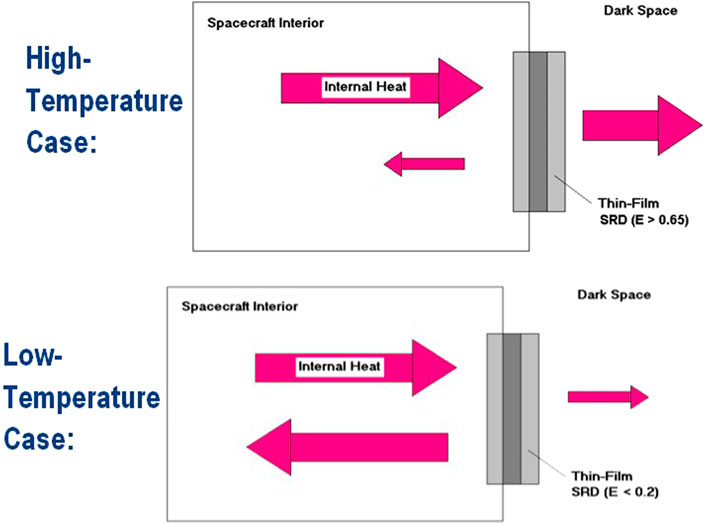
FIGURE 1. Principle of the smart radiator device- The change in emissivity permits to dissipate the heat at high- temperature and to keep the heat inside spacecraft at low-temperature.
Figure 2 presents the effects of the emissivity on the spacecraft internal temperature. A low IR emissivity such as Al (0.05) keeps the internal temperature above −10°C even at a reduced heat load (2.3 W/m2), i.e., when the radiator is facing the shadow. However, a slight increase of the heat load will increase the temperature above the nominal operational limit of about 50°C. At the other extreme, a high emissivity (0.9) will dissipate a heat load up to 150 (W/m2) before the radiator reaches the limit of 50°C. However, the radiator temperature will go below −10°C, even at an elevated heat load of 60 W/m2, thus requiring an internal heater to protect the payloads.
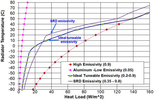
FIGURE 2. Emissivity effect on the radiator temperature due to the heat load Reducing the need to heat the payload to lower Temperature.
An ideal smart radiator device (SRD) would have a low emittance at lower temperatures, and a high emittance at high temperatures, thus maintaining the internal payloads at a moderate temperature under varying conditions. Thin-film coating (V1-x-yMxNyOn) can be applied to existing thermal blankets such as Kapton and Teflon FEP, or to thermal radiators such as Al, to facilitate dynamic thermal control. This approach employs the metal-insulator transition to control heat dissipation and has advantages in terms of weight, cost, integration with the space structure, and structural simplicity (Haddad et al., 2006; Haddad et al., 2009).
5 Deposition and characterization
5.1 First version of smart thermal radiator device (200–300 nm vanadium dioxide)
Undoped and doped VO2 films were prepared in a stainless-steel vacuum chamber by reactive pulsed laser ablation deposition (PLD) using a special target and a XeCl excimer laser. The depositions were performed in a controlled gas-phase background consisting of an O2/Ar gas mixture at total pressures of about 100 mTorr. The substrate temperature was typically held at about 500°C. The film thickness varied from 0.02 to about 0.5 μm.
X-ray diffraction (XRD) was employed to study the structure and stoichiometry of the resulting coatings. Deposition conditions were established for the formation of stoichiometric VO2. X-ray diffraction measurements indicated that high-quality VO2 could be deposited not only on crystalline substrates such as sapphire, where it is lattice-matched, but also on Al.
Characterization was first performed using VO2 deposited on SiO2 (quartz). The reflectance results followed the “intuitive” expectation with high reflectance (R) at high temperatures i.e., low emissivity [ε (λ) = 1−R (λ)]; with no absorption) which is characteristic of a metallic state. For low temperatures, R is low, and ε is high as the VO2 is in semiconductor phase. The reflectance was measured with a Fourier Transform InfraRed spectrometer (FTIR) as presented in Figure 3.
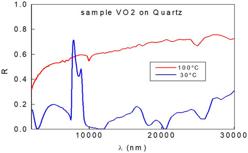
FIGURE 3. Reflectance of the VO2 film deposited on quartz plate measured with FTIR.
For the VO2 deposited on Aluminum, we obtained “counter-intuitive” results: we still have a low reflectance (high ε) at high temperatures and a higher reflectance at (low ε) at lower temperatures, with the transition at the same temperature (around 68°C) as shown in Figure 4. This is an inverse behavior compared with VO2 on Quartz, leading to the question if the VO2 is still in a metallic state at high temperature. The metallic state at high Temperature was confirmed with two measurements (Benkahoul et al., 2011):
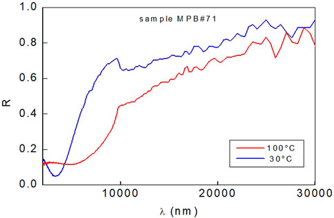
FIGURE 4. Reflectance of the VO2 film deposited on aluminum plate measured with FTIR.
X-ray photoemission spectroscopy (XPS) spectrum of the V3d band of VO2 film deposited on Al substrate. At 30°C (below transition), the spectral weight at Fermi level (EF) is very low which indicates an insulator state. At 100°C, (above transition) the spectral weight at EF is high indicating a metallic behavior. This is similar to what is reported in the literature for VO2/Si and VO2/Quartz.
Raman spectra of the VO2 film on Al. Between 30°C and 55°C narrows Raman peaks are observed. They are attributed to the monoclinic structure. At temperature >70°C only a broad peak centered at about 560 cm−1 is attributed to the tetragonal structure. Between 60°C and 70°C a mixed phase, monoclinic and tetragonal, is formed. This is similar to what is reported in the literature for VO2/Si and VO2/Quartz.
The analysis with Raman spectroscopy and XPS (Figure 5) shows that the VO2 deposited on Aluminum demonstrates is in a metallic state at a high temperature, even if its emissivity is lower, potentially due to the reflectance through an interface that forms between the Al and the VO2 during the VO2 deposition on the Al substrate.
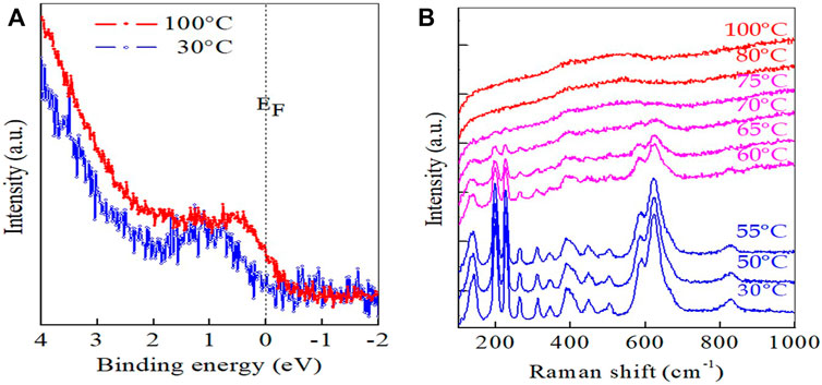
FIGURE 5. Confirming Metallic state at high Temperature (A) with X-ray photoemission spectroscopy (XPS) spectrum of the V3d band of VO2 film deposited on Al substrate; and (B) with Raman shift showing a monoclinic structure at High temperature of VO2 film deposited on Al substrate.
5.2 New approach thin vanadium dioxide (30 nm)
The first version of SRD was based on a 200–300 nm VO2 layer. A previous paper (Haddad et al., 2011) presented the formation of VO2 on aluminum (Al) bulk substrate, on Al or gold (Au) thin layer (100 nm). The Al and Au thin layers were deposited by sputtering and demonstrated the similarity of the two VO2 characteristics, on bulk Al or thin film (Al, Au). The capability of depositing thin Al and Au layers opens the way to use the VO2 on Optical Solar Reflectors currently used in space.
Although in principle there is no evidence of the tuneability (Δε) limitations, experimentally only relatively small to medium value (Δε ≤ 0.35) could be reached. Another challenge is to shift the εH to higher values (≥0.8 and ideally ≥0.9). In previous experimental trials, we could only monitor the lower side of the emissivity εL.
Recently our team (INRS-MPB) succeeded at increasing the Δε and the high emissivity εH using two different approaches. The first method is based on using a relatively thick VO2 (200–300 nm) layer as previously prepared by the team, however with additional layers (Si:H); the second method (Figure 6) (Hendaoui et al., 2013) relies on the interference of thin layer VO2 (20–70 nm) and thick layer SiO2 (1,000–1,500 nm). The two methods were successful, the experimental results are presented in the following sections. The emissivity is sensitive to the buffer thickness
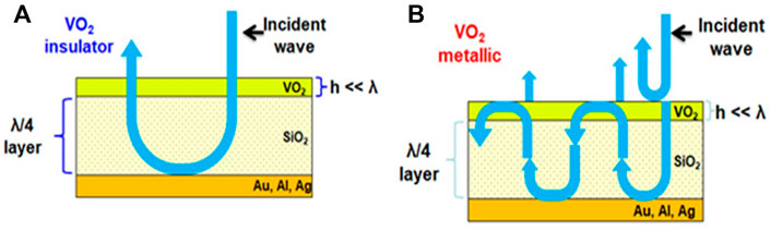
FIGURE 6. Simple schematic explaining the functionality of the VO2- (A) For the VO2 in insulator state, the structure is an IR-reflector (Low emittance); (B) For the VO2 in metallic state, the structure is a reflection interference filter (high emissivity).
5.3 Doping with Tungsten
The intrinsic VO2 transition happens at around 68°C, however, for the SRD application, the transition would be around room temperature (15°C–35°C). The transition temperature was shifted by adding 2.5% of W, to the Vanadium target for the deposition of thin W-VO2 layer. Figure 7 and Table 1 present a summary of the effect of doping the VO2 with W. At 3.5% doping the temperature of the transition is 30°C. This is the optimal % W without losing part of the tuneability
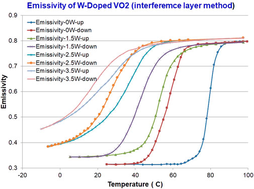
FIGURE 7. Evolution of the SRD Emissivity as a function of temperature for various %W doping (0%–3.5%).
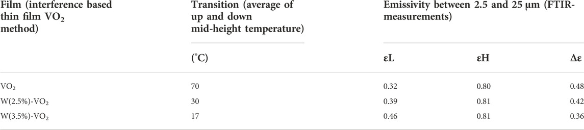
TABLE 1. Effect of W- dopant to VO2 (Emittance = 1−Reflectance) as a function of temperature.
5.4 Solar absorptance
In a previous paper (Haddad et al., 2011), we could reduce the solar absorptance to 0.32 by adding a stacked-layer (λ/4) SiO2/VO2, with λ corresponding to the maximum solar irradiance around 490 nm. The new deposition method is being optimized; Table 2 summarizes the solar absorptance of the various VO2.
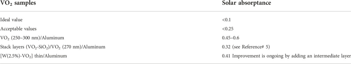
TABLE 2. Comparison of Solar absorptance tests.
5.5 Vanadium dioxide multilayer thin films alternative versions
Three types of SRD were prepared to look for an optimal solution with SRD having good tuneability, acceptable solar reflection, and resistant to harsh space environments:
1) Simple original version: Al/SiO2/VO2-W 2.5%; with manufacturing and relative costs increasing with the number of layers and complexity. Trying to keep manufacturing at a lower cost (called standard in the tests).
2) Added layer on the Aluminum substrate to increase the tuneability of Al/CaF2/SiO2/VO2-W 2.5% (called CaF2 in the tests).
3) Added Si-SiO2 layer as a filter and protective layer Al/SiO2/VO2-W2.5%/SiO2/Si-H (called Si-SiO2 in the tests).
Samples from the three types are used in the tests in particular in the tests determining the SRD emissivities changing with temperature in the vacuum- thermal balance and measured total power and temperatures.
6 Space qualification tests and results
Relatively extensive ground verifications have included Vacuum Accelerated Temperature Aging, Thermal shocks and Thermal Vacuum Cycling (TVAC) testing of the thermal switching under vacuum conditions, vibration testing of Al radiators based on an assembly of the tiles, and some radiation testing relevant to use in a geostationary (GEO) orbit environment. The SRD has successfully passed the major ground tests and validated its performance for extended use in the harsh space environment with a target of over 10 years GEO. With no mechanical moving components, reliable long-term performance is anticipated for this SRD technology. The test follows the ESA testing standards, ECSS-Q-ST-70-17C (ECSS, 2020), and the thermo-optical properties performance of the samples follow ECSS-Q-ST-70-09 (ECSS 2008).
• Thermal Shock 10 cycles: Liquid Nitrogen (LN2 @-196°C), and oven at 120°C dwell time 10 min.
• Test Adhesion: two samples with Scotch tape 3–600 M in the center
• Temperature cycling between −25°C and 60°C, 1,100 cycles
• Accelerated Temperature Aging at 110°C, Measurement after 1,000 h and after 1,750 h
• Humidity test equivalent to 4 years storage at 21°C and 52.5% Relative humidity
• The details of the tests were presented in a previous paper (Haddad et al., 2020). In all the tests performed, the emissivity was measured with an Infrared spectrometer, with an accuracy of ±0.01
The thermal shock is not required for space qualification. However, a thin film that passes it successfully is an indication of long-time stability. We performed 10 cycles of Thermal Shock between Liquid Nitrogen (LN2 at −196°C) bath and oven at 110°C with a dwell time of 10 min and less than 20 s transfer time. The thermal shock test showed no degrading effect on tested SRD samples, the variation on ε remains within the margin of error.
With Thermal Vacuum Cycling (TVAC), a slight loss of performance is observed for some samples but remains too little to conclude on an eventual degradation. In this first test, in vacuum, some samples were slightly bent when detached from the plate for vacuum temperature control. The bending of some samples might have perturbed the Δε measurements but all kinds of SRD seem to be resistant to temperature cycling.
With Accelerated Temperature Aging, no performance loss has been observed on the tested samples. All kinds of SRD seem to be resistant to Temperature aging. Consecutive tests (temperature cycling then temperature aging) show no effect on the SRD. The second measurement after 1,750 h confirms the SRD resistance to temperature aging. We think the observed variations in absolute emissivity values arise from the bending of some samples.
For the Adhesion-Delamination test, ESA requires a medium-strength test corresponding to Scotch tape 3–600 M (3–4 N/cm), with a peeling speed of 2.5 mm/s at a 90° angle. Three virgin SRD samples were tested, two with Scotch tape 3–600 M in the center, and one with Kapton tape 3M5413 (5.8 N/cm). Then we tested an additional three samples that had undergone Thermal Vacuum and Accelerated temperature aging test. We noticed a slight decrease in performance (Δε) on some tested samples with medium strength 3–600 M, but this may be due to measurement error. With the stronger 3M5413, a considerable fraction, about 50% of the tuneability is lost. That could be explained by a slight loss of thermochromic VO2 material atop the sample.
The purpose of the humidity test is to demonstrate the ability of the SRD to withstand exposure to a humid environment during storage before launch. The recent ECSS-Q-ST-70-17C, related to Durability testing of coatings proposes the humidity test for coatings thicker than 1 μm, 7 days, at 50°C/95% RH (Chicarell et al., 2016), and equivalent to 4 years of storage in a cleanroom at 21°C and 52.5% RH. The first samples tested were affected by the humidity test, to our surprise. We think the reason is the 50C is still in the phase transition which is affecting the test result. We opted to find alternative tests at a different temperature.
The accelerated temperature aging test due to temperature is based on the equation of Arrhenius for the temperature and the equation of Hallberg-Peck for the temperature combined with humidity. Arrhenius equation relates to how increased temperature accelerates the age of a product as compared to its normal operating temperature. Hallberg—Peck models the effect of temperature and humidity combined on product life. It uses the Arrhenius equation with an acceleration factor due to the Humidity stress.
Af = Acceleration factor
RHu = use environment relative humidity
RHt = test environment relative humidity
Ea = activation energy in electron-volts (eV) usually it is 1 eV
k = Boltzmann’s constant (k = 5.670 × 10⁻⁸ Wm−2K−4).
Tu = Reference temperature, in Kelvin (K = C + 273).
Tt = Temperature during test, in Kelvin
e = 2.71828 (base of the natural logarithms).
The exponent coefficient of (RHt/RHu), is set to 3 as is commonly used, although 4.5 is used for semiconductors.
The above equation gives the humidity ECSS test (7days, 50°C, 95% RH); the obtained equivalent storage lifetime (21°C and 52.5% RH) is 4 years. MPB tested a few SRD samples at various temperatures >60°C and RH in the range 70%–75%. The test duration is equivalent to 4 years of storage time at 21°C and 52.5% RH. All the SRD samples, including the new alternatives, successfully passed the humidity test, without changes in the emissivity. To confirm the validity, some samples successfully passed a second and even a third humidity alternative without being affected.
7 Measurements of emissivity by thermal balance, comparison with infrared measurements
The SRD performance has been validated in an LN2-cooled thermal vacuum chamber using different heat loads for SRD temperatures between −60°C and +80°C. In comparison to the case of a fixed-emissivity radiator, a much lower overall temperature variation of the system is possible using the passively-tuned SRD radiator.
The total power received by the block and sample (Q-total) is emitted by radiation through the top surface of the sample under testing (Q-top), the bottom with either electrical Kapton heating sheet, the MLI or the same SRD (Q-bottom) and through the lateral (Q-lateral).
σ is the Stephan-Boltzmann constant = 5.670 × 10⁻⁸ (Wm−2K−1).
A is the Surface area (m2).
Th is the hot body temperature (K)—the block in our case
Tc is the cold body temperature (K)- the shroud cooled by LN2 in our case
The top, bottom, and lateral areas are each 4 cm × 4 cm—hence A is the same for each sample or reference.
Th and Tc are given by the corresponding Thermocouple reading
Assuming we know εbottom and εlat We can deduce εtop
Q-total is given by the applied electrical power in W.εbottom of the Kapton h/resistor heater, and for the MLI is about 0.8–0.9.
Table 3 summarizes the four tests performed in vacuum to calculate the emissivities of the SRD from the measured temperatures and total power. In all the tests the cooling was monitored with LN2, along with the SRD samples two sample witnesses one with high emissivities (Acktar black thin sheet, εAcktar = 0.9) sensitive at high temperature, and one with the bared Aluminium substrate of the SRD (εAl = 0.1) sensitive at low temperatures.
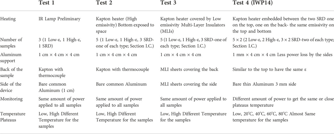
TABLE 3. Comparison of the four TVAC tests, the improvement is in bold.
Each test includes improvements compared with the previous one, indicated in bold characters.
In Test 2, Test 3, and Test 4 we used three different SRD one of each type—standard, with CaF2 or with an S-SiO2 top layer (Section 5.5). In Test4 the same emissivity on top and bottom is used to improve the measurement accuracy.
Figure 8 illustrates the disposition of the five samples tested in Test 3 and Test 4.
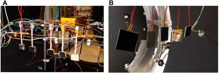
FIGURE 8. (A) Picture of the five samples attached inside DTVAC in Test 3 (B) Picture of five double-sided SRD samples for test 4, the top and back surfaces were similar samples to increase the surfaces.
Figure 9 presents the emissivity values of the five samples obtained from the thermal balance during three plateaus of temperatures, in Test4, and they are compared with the emissivities given by IR Reflectance.
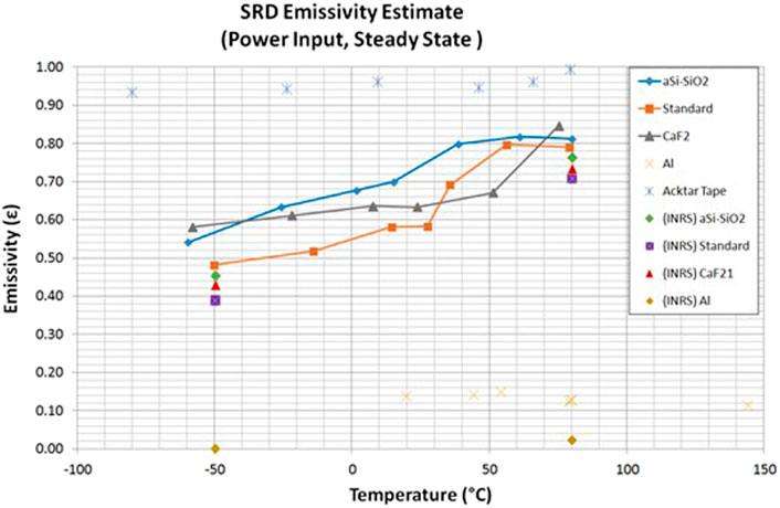
FIGURE 9. Emissivities of the five samples obtained at the plateaus (steady-state power equilibrium).
The values follow the trend, we can see the switching of the SRD but both emissivities low and high have slightly higher values than those measured by IR spectrometer. The emissivity of the SRD follows the same trend as that measured by IR spectrometers.
Assumptions were used for several variables to determine the emissivity at any given temperature. Due to possible errors in these assumptions a transient analysis was done on the thermal response of the SRD samples during Test4. The SRD samples were held at a steady-state at roughly 80°C under vacuum and surrounding LN2 temperature environment. Then the power was shut off to the heaters and the SRDs were radiatively cooled by the LN2 wall. Once SRD samples reached −80°C, the power was turned back on at each sample and steady-state was reached again. From this data, the theoretical and experimental temperature response curves were plotted and variables based on initial assumptions were iteratively modified. Figure 10 displays the transient response data used to optimize the emissivity response estimate. During steady-state plateaus, the differences between model and experimental temperatures were minimal (below 3°C), while the cooldown showed the largest difference. Table 4 presents the average temperature difference (model and experimental temperature), during the cooldown period, of all five samples in Test4. This shows a good correlation for the simulation model for all samples except CaF2.
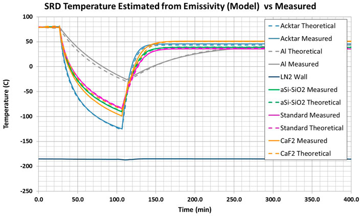
FIGURE 10. Cool-down and heating curve for Test 4 SRD transient analysis.

TABLE 4. Average Errors in temperature calculating the temperature from the emissivities.
8 Conclusion and next steps
The smart radiator device is complying with the space environment requirements. The main objective is to lead the progress in the device preparation toward a commercial product:
• Increase the deposition size to obtain a larger VO2-based smart radiator device. Recent papers show important improvement in some of the deposition processes such as the deposition of a Vanadium layer by magnetron sputtering starting from Vanadium nitride target, or dip coating sol-gel with a temperature at around 350°C
• Decrease the Vanadium deposition temperature to facilitate the process, and permit the deposition on flexible materials such as polyimide (Kapton) or composites; it is possible to have commercial polyimide sheets with a metallic coating (Al, Ge, Ag, Au, …) as an interface between the polyimide and the VO2, opening the way to novel applications in space
• Increase the emissivity tuneability, recent papers showed a large tuneability obtained with a special interface layer
• Reduce the cost toward an affordable cost.
MPB is looking forward to a flight demonstration of the SRD technology on one of the Cubesat missions, and building collaborations to extend the expertise in the VO2 preparation and characterization toward other innovative applications.
Author contributions
EH is the project manager at MPB, he participated in the analysis and wrote the paper. RK is a senior scientist who started the VO2 projects and is participating in the product innovation and progress as well as in the analysis of the results. PM prepared the experimental set-up and the software codes for the data acquisition (in vacuum chamber). WJ was the director of the group who guided all the main contracts and projects. KT is the engineer who took the measurements and did the first steps of the analysis. MC is the manager of the project collaboration at INRS. BL did all the deposition multilayer and looked for the optimal options.
Conflict of interest
Authors EH, RK, PM, WJ, and KT were employed by MPB Communications Inc.
The remaining authors declare that the research was conducted in the absence of any commercial or financial relationships that could be construed as a potential conflict of interest.
Publisher’s note
All claims expressed in this article are solely those of the authors and do not necessarily represent those of their affiliated organizations, or those of the publisher, the editors and the reviewers. Any product that may be evaluated in this article, or claim that may be made by its manufacturer, is not guaranteed or endorsed by the publisher.
References
Aetukuri, N. B., Gray, A. X., Drouard, M., Cossale, M., Gao, L., Reid, A. H., et al. (2013). Control of the metal-insulator transition in vanadium dioxide by modifying orbital occupancy. Nat. Phys. 9, 661.
Araki, Ken, and Zhang, Richard Z. (2022). Simultaneous solar rejection and infrared emission switching using an integrated dielectrics-on-VO2 metasurface featured. AIP Adv. 12, 055205. doi:10.1063/5.0085111
Basu, Raktima, Mangamma, G., and Dhara, Sandip (2021). Novel observation of piezoelectricity in VO2. doi:10.48550/arXiv.2109.07089
Baum, S., Yang, D. S., and Zewail, A. H. (2007). 4D visualization of transitional structures in phase transformations by electron diffraction. Science 318, 788–792. doi:10.1126/science.1147724
Belyaev, Maksim, Boriskov, Petr, Velichko, Andrei, Khanin, S. D., Putrolainen, V. V., Ryabokon’, D. V., et al. (2018). Switching Channel development dynamics in planar structures on the basis of vanadium dioxide. Phys. Solid State 60 (3), 447–456. doi:10.1134/S1063783418030046
Ben-Abdallah, Philippe, and Biehs, Svend-Age (2016). Towards Boolean operations with thermal photons. Phys. Rev. B 94, 241401. doi:10.1103/PhysRevB.94.241401
Benkahoul, M., Chaker, M., Margot, J., Haddad, E., Kruzelecky, R., Wong, B., et al. (2011). Thermochromic VO2 film deposited on Al with tunable thermal emissivity for space applications. Sol. Energy Mater. Sol. Cells 95, p3504–p3508. doi:10.1016/j.solmat.2011.08.014
Bergamini, L., Chen, B., Traviss, D., Wang, Y., and Groot, C. H. de. (2021). Single-nanoantenna driven nanoscale control of the VO2 insulator to metal transition. Nanophotonics 10 (14), 3745–3758. doi:10.1515/nanoph-2021-0250
Birur, G. C., Waniewski Sur, T., Paris, A., Shakkottai, P., Green, A., Haapanen, S., et al. (2001). “Micro/nano spacecraft thermal control using a MEMS-based pumped liquid cooling system”,” in Presented at SPIE conference on Micromachining and Microfabrication, San Francisco, USA, October 21-24, 2001.
Biter, W., Oh, S., and Hess, S. (2002). “Electrostatic switched radiator for space based thermal control,” in Proceedings of the Space Technology and Applications International Forum; (STAIF), Albuquerque, NM.
Bragaggia, G., Cacciatore, A., Poffe, E., Capone, C., Zorzi, F., Causin, V., et al. (2021). Systematic exploration of the synthetic parameters for the production of dynamic VO2(M1). Molecules 26 (15), 4513. doi:10.3390/molecules26154513
Brassard, D., Fourmaux, S., Jean-Jacques, M., Kieffer, J. C., and El Khakani, M. A. (2005). Grain size effect on the semiconductor-metal phase transition characteristics of magnetron-sputtered VO2 thin films. Appl. Phys. Lett. 87, 051910. doi:10.1063/1.2001139
Brinker, C. J. (2013). “Dip coating,” in Chemical solution deposition of functional oxide thin films”. Editors T. Schneller, R. Waser, M. Kosec, and D. Payne (Vienna: Springer Vienna), 233–261. doi:10.1007/978-3-211-99311-8_10
Cavalleri, T., Tóth, C. S., Siders, C. W. J. A., Squier, J. A., Rakzi, F., Forget, P., et al. (2001). Femtosecond structural dynamics inVO2during an ultrafast solid-solid phase transition. Phys. Rev. Lett. 87, 237401. doi:10.1103/physrevlett.87.237401
Chang, Tianci, Zhu, Ying, Cao, Cuicui, Yang, Chunlei, Luo, Hongjie, Jin, Ping, et al. (2021). Multifunctional flexible vanadium dioxide films. Acc. Mat. Res. 2 (9), 714–725. doi:10.1021/accountsmr.1c00044
Chicarell, L., Tighe, A., Durin, C., Amar, C., Semprimoschnig, C., Renard, E., et al. (2016). New ECSS standard for environmental durability testing of optical coatings for space application. France: ICSO, Biarritz, 18–21.
Chudnovskii, F. A., Kikalov, D. O., Pergament, A. L., and Stefanovich, G. B. (1999). Electrical transport properties and switching in vanadium anode oxides: Effect of laser irradiation. Phys. Stat. Sol. A 172, 391.
Corti, Elisabetta (2021). Networks of coupled VO2 oscillators for neuromorphic computing”. Ph.D. Thesis (Switzerland: EPFL).
Cueff, S., Li, D., Zhou, Y., Wong, F. J., Kurvits, J. A., Ramanathan, S., et al. (2015). Dynamic control of light emission faster than the lifetime limit using VO2 phase-change. Nat. Commun. 6, 8636. doi:10.1038/ncomms9636
Cui, Y., Ke, Y., Liu, C., Chen, Z., and Wang, N. (2018). Review thermochromic VO2 for energy-efficient smart windows. Joule 2, 1707–1746. doi:10.1016/j.joule.2018.06.018
Currie, Marc, Mastro, Michael A., and Wheeler, Virginia D. (2017). Characterizing the tunable refractive index of vanadium dioxide. Opt. Mat. Express 7, p1697–p1707. doi:10.1364/OME.7.001697
Dachuan, Y., Niankan, X., Jingyu, Z., and Xiulin, Z. (1996). Vanadium dioxide films with good electrical switching property. J. Phys. D. Appl. Phys. 29 (4), 1051–1057. doi:10.1088/0022-3727/29/4/017
Dudon, J. P., Marcel, C., Dubost3, L., Ravaux, A., Aubert, P. H., Duzellier, S., et al. (2021). “Development of variable emissivity coatings for thermal radiator,” in 50th International Conference on Environmental Systems ICES-2021-63, 12-15 July.
Eaton, Miller, Catellani, Alessandra, and Arrigo, Calzolari (2018). VO2 as a natural optical metamaterial. Opt. Express 26, 5342–5357. doi:10.1364/oe.26.005342
Egorov, F. A., Temirov, Y. S., Sokolovskii, A. A., Dvoryankin, V. F., Kukhta, A. V., and Starostin, N. I. (1991a). Optically controlled fiber optic switch based on a VO2 film. Sov. Tech. Phys. Lett. 17, 345–346.
Egorov, F. A., et al. (1991b). Controllable fiber-optic light modulator based on vanadium dioxide. Sov. Tech. Phys. Lett. 17, 817–819.
Fan, L. L., Chen, S., Wu, Y. F., Chen, F. H., Chu, W. S., Chen, X., et al. (2013). Growth and phase transition characteristics of pure M-phase VO2 epitaxial film prepared by oxide molecular beam epitaxy. Appl. Phys. Lett. 103, 131914. doi:10.1063/1.4823511
Fan, Xiaofei, Wei, Guodong, Lin, Xiaoyang, Wang, Xinhe, Si, Zhizhong, Zhang, Xueying, et al. (2020). Reversible switching of interlayer exchange coupling through atomically thin VO2 via electronic state modulation. Matter 2, 1582–1593. doi:10.1016/j.matt.2020.04.001
Feng, Y.-Q., Lv, M.-L., Yang, M., Ma, W.-X., Zhang, G., Yu, Y.-Z., et al. (2022). Application of new energy thermochromic composite thermosensitive materials of smart windows in recent years. Molecules 27, 1638. doi:10.3390/molecules27051638
Fowlie, Jennifer, Georgescu, A. B., Mundet, Bernat, del Valle, P., and Tückmantel, Philippe (2021). Machines for materials and materials for machines: Metal-insulator transitions and artificial intelligence. Front. Phys., 15, doi:10.3389/fphy.2021.725853
Franke, E., Neumann, H., Schubert, M., Trimble, C., Yan, L., and Woollam, J. (2002). Low-orbit-environment protective coating for all-solid-state electrochromic surface heat radiation control devices. Surf. Coat. Technol. 151-152, 285–288. doi:10.1016/s0257-8972(01)01608-5
Gao, Xing, Carlos, M. M., and Hilgenkampa, Hans (2022). Multi-level operation in VO2-based resistive switching devices. AIP Adv. 12, 015218. doi:10.1063/5.0077160
García-Wong, A. C., Pilloud, D., Bruyère, S., Mangin, D., Migot, S., Pierson, J. F., et al. (2021). Surface morphology-optical properties relationship in thermochromic VO2 thin films obtained by air oxidation of vanadium nitride. J. Materiomics 7, p657–p664. doi:10.1016/j.jmat.2020.12.005
García-Wong, A. C., Pilloud, D., Bruyère, S., Mathieu, S., Migot, S., Pierson, J. F., et al. (2020). Oxidation of sputter-deposited vanadium nitride as a new precursor to achieve thermochromic VO2 thin films. Sol. Energy Mat. Sol. Cells 210, 110474. doi:10.1016/j.solmat.2020.110474
Gilmore, D. G. (1994). Satellite thermal control handbook. El Segundo, California: The Aerospace Corporation Press.
Granqvist, C. G., Azens, A., Hjelm, A., Kullman, L., Niklasson, G. A., Rönnow, D., et al. (1998). Recent advances in electrochromics for smart windows applications. Sol. Energy 63, 199–216. doi:10.1016/S0038-092X(98)00074-7
Gray, A. X., Hoffmann, M. C., Jeong, J., Aetukuri, N. P., Zhu, D., Hwang, H. Y., et al. (2018). Ultrafast terahertz field control of electronic and structural interactions in vanadium dioxide. Phys. Rev. B 98, 045104. doi:10.1103/PhysRevB.98.045104
Guinneton, L., Sauques, J. C., Valmalette, F., Crosa, J. R., and Gavarri, J. R. (2001). Comparative study between nanocrystalline powder and thin film of vanadium dioxide VO2: electrical and infrared properties. Journal of Physics and Chemistry of Solids 62, 1229 + 1238–295. doi:10.1016/j.tsf.2003.09.062
Guinneton, F., Sauques, L., Valmalette, J.-C., Crosa, F., and Gavarri, J.-R. (2004). Optimized infrared switching properties in thermochromic vanadium dioxide thin films: Role of deposition process and microstructure. Thin Solid Films 446, 287–295. doi:10.1016/j.tsf.2003.09.062
Haddad, E., BenKahoul, M., Kruzelecky, R. V., Wong, B., Jamroz, W., Soltani, M., et al. (2011). “Monitoring thermo-optical properties of multilayer tuneable emittance coatings for smart thermal control in space,” in 41st International Conference on Environmental Systems, Oregon.
Haddad, E., Kruzelecky, R. V., Brian Wong, B., Jamroz, W., Hendaoui, A., Chaker, M., et al. (2013). “Large tuneability IR emittance thermal control coating for space applications,” in AIAA- 43rd International Conference on Environmental Systems, July 14-18. doi:10.2514/6.2013-3436
Haddad, E., Kruzelecky, R. V., Wong, B., Jamroz, W., Soltani, M., Chaker, M., et al. (2006). “Multi-function tuneable emittance smart coatings for thermal control in harsh space environment,” in ICES, 36th International Conference on Environmental Systems, Norfolk, Virginia, USA, July 11-14.
Haddad, E., Kruzelecky, R. V., Wong, B., Jamroz, W., Soltani, M., Chaker, M., et al. (2009). “Multilayer tuneable emittance coatings with low solar absorptance for improved smart thermal control in space applications,” in 39th International Conference on Environmental Systems, Savannah, Georgia, USA, July 12-16.
Haddad, Emile, Kruzelecky, Roman V., Murzionak, Piotr, Kamel, Tagzeria, Paul, Burbulea, Schinn, I. S. G., et al. (2020). “VO2-based thin-film smart radiator device for improved passive thermal control of space systems,” in 50th International Conference on Environmental Systems.
Hendaoui, A., Chaker, M., and Haddad, E. (2014). Passively variable emittance device and method for making the same. Patent.
Hendaoui, A., Émond, N., Haddad, E., and Chaker, M. (2013). Highly tunable-emittance radiator based on semiconductor-metal transition of VO2 thin films. Appl. Phys. Lett. 102, 061107. doi:10.1063/1.4792277
Ho, H. C., Lai, Y. C., Chen, K., Thang Duy Dao, H. N., Hsueh, C. H., and Nagao, T. (2019). High quality thermochromic VO2 films prepared by magnetron sputtering using V2O5 target with in situ annealing. Appl. Surf. Sci. 495, 143436. doi:10.1016/j.apsusc.2019.07.178
Houska, J., Kolenaty, D., Vlcek, J., and Cerstvy, "R. (2018). Properties of thermochromic VO2 films prepared by HiPIMS onto unbiased amorphous glass substrates at a low temperature of 300C. Thin Solid Films 660, 463–470. doi:10.1016/j.tsf.2018.06.057
Hu, Changlong, Liang, Li, Wen, Xiaolei, Chen, Yuliang, Li, Bowen, Ren, Hui, et al. (2021). Manipulating the anisotropic phase separation in strained VO2 epitaxial films by nanoscale ion-implantation. Appl. Phys. Lett. 119, 121101. doi:10.1063/5.0060739
Ionescu, A. (2018). “Chapter 8 - beyond CMOS: Steep-slope devices and energy efficient nanoelectronics,” in High mobility materials for CMOS applications (Woodhead Publishing Series in Electronic and Optical Materials), 281–305. doi:10.1016/B978-0-08-102061-6.00008-2
Iqbal, S., Duy, L. T., Kang, H., Singh, R., Kumar, M., Park, J., et al. (2021). Femtojoule-power-consuming synaptic memtransistor based on Mott transition of multiphasic vanadium oxides. Adv. Funct. Mat. 31 (46), 2102567. doi:10.1002/adfm.202102567
Jiang, H., Wang, Y., Cui, Z., Zhang, X., Zhu, Y., and Zhang, K. (2022). Vanadium dioxide-based terahertz metamaterial devices switchable between transmission and absorption. Micromachines 13, 715. doi:10.3390/mi13050715
Johnston, R. L. (1998). The development of metallic behaviour in clusters. Philosophical Trans. R. Soc. Lond. Ser. A Math. Phys. Eng. Sci. 356, 211–230. doi:10.1098/rsta.1998.0158
Jung, Youngho, Han, Hyeon, Sharma, Ankita, Jeong, Junho, Stuart, S., Parkin, P., et al. (2022). Integrated hybrid VO2–silicon optical memory. ACS Photonics 9 (1), 217–223. doi:10.1021/acsphotonics.1c01410
Jung, Youngho, Jeong, Junho, Qu, Zhongnan, Cui, Bin, Khanda, Ankita, Stuart, S. P., et al. (2021). Observation of optically addressable nonvolatile memory in VO2 at room temperature. Adv. Electron. Mat. 7, 2001142. doi:10.1002/aelm.202001142
Kabir, Sumaiya, Nirantar, Shruti, Zhu, Liangchen, Ton-That, Cuong, Jain, S. K., Kayani, A, B. A., et al. (2020). Phase change vanadium dioxide light sensors. Appl. Mater. Today 21, 100833. doi:10.1016/j.apmt.2020.100833
Kats, Mikhail A., Blanchard, Romain, Zhang, Shuyan, Genevet, Patrice, Ko, Changhyun, Ramanathan, Shriram, et al. (2013). Vanadium dioxide as a natural disordered metamaterial: Perfect thermal emission and large broadband negative differential thermal emittance. Phys. Rev. X 3, 041004. doi:10.1103/PhysRevX.3.041004
Kim, Heungsoo, Kwok, Cheung, Raymond, C., Auyeung, Y., Wilson, Donald E., Charipar, Kristin M., et al. (2019). VO2-based switchable radiator for spacecraft thermal control. Sci. Rep. 9, 11329. doi:10.1038/s41598-019-47572-z
Kim, Jaekyung, Seong, Junhwa, Yang, Younghwan, Moon, Seong-Won, Badloe, Trevon, and Rho, Junsuk (2022). Tunable metasurfaces towards versatile metalenses and metaholograms: A review. Adv. Photonics 4. doi:10.1117/1.AP.4.2.024001
Kruzelecky, R., Haddad, E., and Wong, B. (2010). Variable emittance thermochromic material and satellite system. Patent 761, 053B2.
Kruzelecky, R. V., Haddad, E., Jamroz, W., Soltani, M., Chaker, M., Nikanpour, D., et al. (2005). “Thin-film smart radiator tiles with dynamically tuneable thermal emittance,” in Society of Automotive Engineers, Inc. Proceeding, Rome, Italy, July 11-14, 2005.
Kumi-Barimah, E., Anagnostou, D. E., and Jose, G. (2020). Phase changeable vanadium dioxide (VO2) thin films grown from vanadium pentoxide (V2O5) using femtosecond pulsed laser deposition. AIP Adv. 10 (6), 065225. doi:10.1063/5.0010157
Lan, Xiaohua, Wang, Yi, Peng, Jiebin, Yang, Si, Ren, Jie, Ding, Bin, et al. (2021). Designing heat transfer pathways for advanced thermoregulatory textiles. Mater. Today Phys. 17, 100342. doi:10.1016/j.mtphys.2021.100342
Latella, Ivan, Biehs, Svend-Age, and Ben-Abdallah, Philippe (2021). Smart thermal management with near-field thermal radiation. Opt. Express 29 (16), 24816.
Li, Xike, Tang, Shiwei, Ding, Fei, Zhong, Shuomin, Yang, Yuanqing, Jiang, Tao, et al. (2019). Switchable multifunctional terahertz metasurfaces employing vanadium dioxide. Sci. Rep. 9, 5454. doi:10.1038/s41598-019-41915-6
Liu, Kai, Lee, Sangwook, Yang, Shan, Olivier, Delaire, and Wu, Junqiao (2018). Recent progresses on physics and applications of vanadium dioxide. Mater. Today 21, 875–896. doi:10.1016/j.mattod.2018.03.029
Liu, T. H., Han, X., Pastrana, J., Sepúlveda, N., and Wang, J. (2022). Piezoelectric lateral-extensional mode resonators with reconfigurable electrode and resonance mode-switching behavior enabled by a VO₂ thin-film. IEEE Trans. Ultrason. Ferroelectr. Freq. Control 69, 2512–2525. doi:10.1109/TUFFC.2022.3156845
Lu, X., Sun, Y., Chen, Z., and Gao, Y. (2017). A multi-functional textile that combines self-cleaning, water-proofing and VO2-based temperature responsive thermoregulating. Sol. Energy Mat. Sol. Cells 159, 102–111. doi:10.1016/j.solmat.2016.08.020
Ma, W., Zidan, M. A., and Lu, W. D. (2018). Neuromorphic computing with memristive devices. Sci. China Inf. Sci. 61 (6), 060422. doi:10.1007/s11432-017-9424-y
Manousou, Dimitra K., Gardelis, Spiros, Calamiotou, Maria, and Syskakis, Emmanuel (2021). VO2 thin films fabricated by reduction of thermal evaporated V2O5 under N2 flow. Mater. Lett. 299, 130086. doi:10.1016/j.matlet.2021.130086
Meng, Haiyu, Wang, Lingling, Liu, Ziran, Chen, Jianghua, and Lee, Ching Hua (2022). Port reconfigurable phase-change optical resonator.
Merced, Emmanuelle, Tan, Xiaobo, and Nelson, Sepúlveda (2013). Strain energy density of VO2-based microactuators. Sensors Actuators A Phys. 196, 30–37. doi:10.1016/j.sna.2013.02.029
Mirbagheri, G., Crouse, D. T., and Tan, C.-K. (2022). Recent advance in phase transition of vanadium oxide based solar reflectors and the fabrication progress”. SPIE Photonics West Opto.
Mizsei, J., Bein, Marton C., Lappalainen, Jyrki, Plesz, Balázs, and Plesz, B. (2015). The phonsistor – a novel VO2 based nanoscale thermal-electronic device and its application in thermal-electronic logic circuits (telc). Mater. Today Proc. 2 (8), 4272–4279. doi:10.1016/j.matpr.2015.09.013
Molaei, R., Bayati, R., Nori, S., Kumar, D., Prater, J. T., and Narayan, J. (2013). Diamagnetic to ferromagnetic switching in VO2 epitaxial thin films by nanosecond excimer laser treatment. Appl. Phys. Lett. 103, 252109. doi:10.1063/1.4857155
Morin, F. (1959). Oxides which show a metal-to-insulator transition at the neel temperature. Phys. Rev. Lett. 3, 34–36. doi:10.1103/physrevlett.3.34
Muller, A. A., Moldoveanu, A., Asavei, V., Khadar, R. A., Sanabria-Codesal, E., Krammer, A., et al. (2019). 3D Smith charts scattering parameters frequency-dependent orientation analysis and complex-scalar multi-parameter characterization applied to Peano reconfigurable vanadium dioxide inductors. Sci. Rep. 9, 18346. doi:10.1038/s41598-019-54600-5
Osiander, R., Champion, J., Darrin, M., Allen, J. J., Douglas, D., and Swanson, T. (1999). Micro-machined shutter arrays for thermal control radiators on ST5. AIAA-2002-0359. doi:10.2514/6.2002-359
Outon, J., Blanco, E., Domínguez, M., Bakkali, H., Gonzalez-Leal, J. M., Delgado, J. J., et al. (2022). Tracking the optical constants of porous vanadium dioxide thin films during metal–insulator transition: Influence of processing conditions on their application in smart glasses. Appl. Surf. Sci. 580, 152228.
Papari, G. P., Pellgrino, A. L., Malandrino, Graziella, and Andreone, Antonello (2022). Sensing enhancement of a Fabry-Perot THz cavity using switchable VO2 mirrors. Opt. Express 30, 19402–19415. doi:10.48550/arXiv.2202.00921
Peng, Linghui, Shen, Lingling, Fan, Weiren, Liu, Zichuan, Qiu, Hongbo, Yu, Aibing, et al. (2021). Ag/VO2/Ag sandwich nylon film for smart thermal management and thermo-responsive electrical conductivity. J. Industrial Text.
Peng, Linghui, Su, Bin, Yu, Aibing, and Jiang, Xuchuan (2019). Review of clothing for thermal management with advanced materials. Cellulose 26, 6415–6448. doi:10.1007/s10570-019-02534-6
Pergament, A. L., Boriskov, P. P., Velichko, A. A., and Kuldin, N. A. (2010). Switching effect and the metal-insulator transition in electric field. J. Phys. Chem. Solids 71, 874–879. doi:10.1016/j.jpcs.2010.03.032
Pergament, A. L., Stefanovich, G. B., and Velichko, A. A. (2013). Oxide electronics and vanadium dioxide perspective: A review. J. Sel. Top. Nano Electron. Comput. 1, 24–43. doi:10.15393/j8.art.2013.3002
Pergament, A., Stefanovich, G., Malinenko, V., and Velichko, A. (2015). Electrical switching in thin film structures based on transition metal oxides. Adv. Condens. Matter Phys. 2015, 1–26. doi:10.1155/2015/654840
Pergament, A., Stefanovich, G., Velichko, A., Putrolainen, V., Kundozerova, T., and Stefanovich, Т. (2020). Novel hypostasis of old materials in oxide electronics metal oxides for resistive random access memory applications book 7x10 - template - version_15.
Pósa, L., Molnár, G., Kalas, B., Baji, Z., Czigány, Z., Petrik, P., et al. (2021). A rational fabrication method for low switching-temperature VO2. Nanomaterials 11, 212. doi:10.3390/nano11010212
Prakash, Pitchappa, Kumar, Abhishek, Singh, Ranjan, Lee, Chengkuo, and Wang, Nan (2021). Terahertz MEMS metadevices. J. Micromech. Microeng. 31, 113001–21pp. doi:10.1088/1361-6439/ac1eed
Prasadam, V. P., Bahlawane, N., Mattelaer, F., Rampelberg, G., Detavernier, C., Fang, L., et al. (2019). Atomic layer deposition of vanadium oxides: Process and application review. Mat. Today Chem. 12, 396–423. doi:10.1016/j.mtchem.2019.03.004
Qaderi, F., Rosca, T., Burla, M., Leuthold, J., Flandre, D., and Ionescu, A. (2021). Millimeter- and Terahertz-wave stochastic sensors based on reversible insulator-to-metal transition in vanadium dioxide. Res. square. doi:10.21203/rs.3.rs-126738/v1
Rampelberg, Geert (2016). Thin film synthesis of VO2 and VN by gas-solid reactions and atomic layer deposition”. Ph.D. Thesis (Ghent, Belgium: Ghent University Belgium).
Ruzmetov, D., Zawilski, K. T., Senanayake, S. D., Narayanamurti, V., and Ramanathan, S. (2008). Infrared reflectance and photoemission spectroscopy studies across the phase transition boundary in thin film vanadium dioxide. J. Phys. Condens. Matter 20, 465204. doi:10.1088/0953-8984/20/46/465204
Ryckman, J. D., Hallman, K. A., Marvel, R. E., Haglund, R. F., and Weiss, S. M. (2013). Ultra-compact silicon photonic devices reconfigured by an optically induced semiconductor-to metal transition. Opt. Express 21, 10753–10763. doi:10.1364/oe.21.010753
Safi, T. S., Zhang, P., Fan, Y., Guo, Z., Han, J., Rosenberg, E. R., et al. (2020). Variable spin-charge conversion across metal-insulator transition. Nat. Commun. 11, 476. doi:10.1038/s41467-020-14388-9
Santos, A. J., Lacroix, B., Domínguez, M., García, R., Martin, N., and Morales, F. M. (2021). Controlled grain-size thermochromic VO2 coatings by the fast oxidation of sputtered vanadium or vanadium oxide films deposited at glancing angles. Surfaces Interfaces 27, 101581. doi:10.1016/j.surfin.2021.101581
Shao, Z., Cao, X., Luo, H., and Jin, P. (2018). Recent progress in the phase-transition mechanism and modulation of vanadium dioxide materials. NPG Asia Mat. 10, 581–605. doi:10.1038/s41427-018-0061-2
Shimazaki, K., Tachikawa, S., Ohnishi, A., and Nagasaka, Y. (2000). “Design and preliminary test results of variable emittance device,” in Proceedings of the 8th International Symposium on Materials in a Space Environment, Arachon, France.
Soltani, M., Chaker, M., Haddad, E., and Kruzelecky, R. V. (2006). 1×2 optical switch devices based on semiconductor-to-metallic phase transition characteristics of VO2 smart coatings. Meas. Sci. Technol. 17, 1052–1056. doi:10.1088/0957-0233/17/5/s19
Soltani, M., Chaker, M., Haddad, E., Kruzelecky, R. V., and Nikanpour, D. (2004). Optical switching of vanadium dioxide thin films deposited by reactive pulsed laser deposition. J. Vac. Sci. Technol. A 22, 859–864. doi:10.1116/1.1722506
Song, F., and White, B. E. (2016). Growth of ultra-thin vanadium dioxide thin films using magnetron sputtering”.
Stefanovich, G., Pergament, A., and Stefanovich, D. (2000). Electrical switching and Mott transition in VO2. J. Phys. Condens. Matter 12, 8837–8845. doi:10.1088/0953-8984/12/41/310
Sun, Miao, Taha, Mohammad, Walia, Sumeet, Bhaskaran, Madhu, Sriram, Sharath, Shieh, William, et al. (2018). A photonic switch based on a hybrid combination of metallic nanoholes and phase-change vanadium dioxide. Sci. Rep. 8, 11106. doi:10.1038/s41598-018-29476-6
Théry, V., Boulle, A., Crunteanu, A., Orlianges, J. C., Beaumont, A., Mayet, R., et al. (2017). Structural and electrical properties of large area epitaxial VO2 films grown by electron beam evaporation. J. Appl. Phys. 121, 055303. doi:10.1063/1.4975117
Thomas, A., Savaliya, Priten, Kumar, Kamal, Ninawe, Akanksha, and Dhawan, Anuj (2018). Au nanowire-VO2 spacer-Au film based optical switches. J. Opt. Soc. Am. B 35 (7), 1687–1697. doi:10.1364/JOSAB.35.001687
Todri-Sanial, A., Carapezzi, S., Delacour, C., Abernot, M., Gil, T., Corti, E., et al. (2021). How frequency injection locking can train oscillatory neural networks to compute in phase. IEEE Trans. Neural Netw. Learn. Systems”, IEEE. doi:10.1109/TNNLS.2021.3107771
Vaidya, Jaykumar, Kanthi, R. S. Surya, Alam, Shamiul, NazmulAmin, Ahmedullah Aziz, Shukla, Nikhil, and Shukla, N. (2022). A three-terminal non-volatile ferroelectric switch with an insulator–metal transition Channel. Sci. Rep. 12, 2199. doi:10.1038/s41598-021-03560-w
Vernardou, D., Pemble, M. E., and Sheel, D. W. (2004). Vanadium oxides prepared by liquid injection MOCVD using vanadyl acetylacetonate. Surf. Coat. Technol. 188–189, 250–254. doi:10.1016/j.surfcoat.2004.08.037
Victor, J. L., Marcel, C., Sauques, L., Labrugèrec, C., Amiard, F., Gibaud, A., et al. (2021). From multilayers to V1-xWxO2±δ films elaborated by magnetron sputtering for decreasing thermochromic transition temperature. J. Alloys Compd. 858, 157658. doi:10.1016/j.jallcom.2020.157658⟩
Vlcek, J., Kolenatý, D., Houška, J., Kozák, T., and Cerstvý, R. (2017). Controlled reactive HiPIMS—effective technique for low-temperature (300 °C) synthesis of VO2 films with semiconductor-to-metal transition. J. Phys. D. Appl. Phys. 50, 38LT01. doi:10.1088/1361-6463/aa8356
Wang, Q., Zhang, S., Wang, C., Li, R., Cai, T., and Zhang, D. (2021). Tunable infrared optical switch based on vanadium dioxide. Nanomater. (Basel). 11, 2988. doi:10.3390/nano11112988
Wang, S., Kang, L., and Werner, D. H. (2017). Hybrid resonators and highly tunable terahertz metamaterials enabled by vanadium dioxide (VO2). Sci. Rep. 7, 4326. doi:10.1038/s41598-017-04692-8
Wang, X., Qi, H., Hu, X., Yu, Z., Ding, S., Du, Z., et al. (2021). Advances in photonic devices based on optical phase-change materials. Molecules 26, 2813. doi:10.3390/molecules26092813
Wei, L., Kuai, X., Bao, Y., Wei, J., Yang, L., Song, P., et al. (2021). The recent progress of MEMS/NEMS resonators. Micromachines 12, 724. doi:10.3390/mi12060724
Wilson, C. E., Gibson, A. E., Argo, J. J., Loughney, P. A., Xu, W., King, G., et al. (2021). Accelerated microwave-assisted synthesis and in-situ X-ray scattering of tungsten-substituted vanadium dioxide (V1-xWxO2). J. Mater. Res. 36. doi:10.1557/s43578-020-00068-3
Wolfgang, A., Casu, E. A., Biswas, A., Rosca, T., Alper, C., Krammer, A., et al. (2017). A Steep-Slope Transistor Combining Phase-Change and Band-to-Band-Tunneling to Achieve a sub-Unity Body Factor. Nature 7, 355. doi:10.1038/s41598-017-00359-6
Xu, D., Zhao, Junming, and Liu, Linhua (2021). Near-field radiation assisted smart skin for spacecraft thermal control. Int. J. Therm. Sci. 165 (2021), 106934. doi:10.1016/j.ijthermalsci.2021.106934
Xu, X., He, X., Wang, G., Yuan, X., Liu, X., Huang, H., et al. (2011). The study of optimal oxidation time and different temperatures for high quality VO2 thin film based on the sputtering oxidation coupling method. Appl. Surf. Sci. 257, 8824–8827. doi:10.1016/j.apsusc.2011.04.068
Yi, W., Tsang, K. K., Lam, S. K., Bai, X., Crowell, J. A., and Flores, E. A. (2018). Biological plausibility and stochasticity in scalable VO2 active memristor neurons. Nat. Commun. 9, 4661. doi:10.1038/s41467-018-07052-w
Zeng, Hongxin, Gong, Sen, Wang, Lan, Zhou, Tianchi, Zhang, Yaxin, Lan, Feng, et al. (2022). A review of terahertz phase modulation from free space to guided wave integrated devices. Nanophotonics 11 (3), 415–437. doi:10.1515/nanoph-2021-0623
Zhang, Y., Xiong, W., Chen, W., and Zheng, Y. (2021). Recent progress on vanadium dioxide nanostructures and devices: Fabrication, properties, applications and perspectives. Nanomaterials 11, 338. doi:10.3390/nano11020338
Keywords: smart radiator, thermochromic, VO2 applications, vanadium dioxide, satellite/spacecraft thermal control, VO2 phases and transition applications
Citation: Haddad E, Kruzelecky RV, Murzionak P, Jamroz W, Tagziria K, Chaker M and Ledrogoff B (2022) Review of the VO2 smart material applications with emphasis on its use for spacecraft thermal control. Front. Mater. 9:1013848. doi: 10.3389/fmats.2022.1013848
Received: 07 August 2022; Accepted: 18 November 2022;
Published: 15 December 2022.
Edited by:
Rosario Pecora, University of Naples Federico II, ItalyReviewed by:
Jingbo Li, Beijing Institute of Technology, ChinaYongzhi Cheng, Wuhan University of Science and Technology, China
Copyright © 2022 Haddad, Kruzelecky, Murzionak, Jamroz, Tagziria, Chaker and Ledrogoff. This is an open-access article distributed under the terms of the Creative Commons Attribution License (CC BY). The use, distribution or reproduction in other forums is permitted, provided the original author(s) and the copyright owner(s) are credited and that the original publication in this journal is cited, in accordance with accepted academic practice. No use, distribution or reproduction is permitted which does not comply with these terms.
*Correspondence: Emile Haddad, ZW1pbGUuaGFkZGFkQG1wYmMuY2E=