 Hang Yang1,2
 Li Zeng3Ziwei Huang4Tian Zhang5Shunhui Zhang6Xuyang Zhang7Zhikang Ao8Xiang Lan5
 Baihui Zhang6*
- 1Beijing Blue Sky Innovation for Frontier Science, Beijing, China
- 2College of Science, National University of Defense Technology, Changsha, China
- 3Department of Materials Engineering, The University of British Columbia, Vancouver, BC, Canada
- 4Hunan Provincial Key Laboratory of Two-Dimensional Materials, State Key Laboratory for Chemo/Biosensing and Chemometrics, College of Chemistry and Chemical Engineering, Hunan University, Changsha, China
- 5College of Materials Science and Engineering, Hunan University, Changsha, China
- 6College of Physics and Electronics, Central South University, Changsha, China
- 7College of Energy and Power Engineering, Changsha University of Science and Technology, Changsha, China
- 8School of Physical and Mathematical Sciences, Nanjing Tech University, Nanjing, China
The synthesis of two-dimensional lateral heterojunctions with nanoscale characteristic width and sharp interfaces remains challenging. The quantum confinement effects are still difficult to create on 2D materials since widths smaller than 5 nm are necessary for quantum confinement effects and quantum well applications. In this study, we demonstrated the growth of a sub-2-nm tungsten sulfide quantum well array in a monolayer of tungsten selenide, driven by the climb of mismatch dislocation in a heterointerface due to the lattice mismatch. Width-controllable 2D quantum well superlattices are theoretically formed by the mismatch dislocation-driven growth mechanism, according to our analysis. Thus, abundant photonic electronic properties can be obtained in 2D quantum well superlattices formed at varied lateral heterointerfaces, which will support the study of topological insulators and superconductors.
1 Introduction
Two-dimensional (2D) lateral heterojunctions and superlattices with a series of novel properties have been generated and reported recently (Geim and Grigorieva, 2013; Liu et al., 2014; Gong et al., 2015; Li et al., 2015; Zhang et al., 2017; Chen et al., 2018; Liu et al., 2019; Shi et al., 2020; Zhang et al., 2021). Available growth methods produce featured widths in the scale of hundreds of nanometers or, at best, at micrometer scale and commonly result in rough and defective interfaces with extensive chemical intermixing (Li et al., 2015; Liu et al., 2015; Zhang et al., 2017; Shi et al., 2020). Quantum wells in conventional semiconductors with their unique electronic structure and quantum confinement have important applications in quantum cascade lasers, solar cells, high-electron mobility transistors, and infrared photodetectors (Faist et al., 1994; Gudiksen et al., 2002). In a 2D system, quantum well structures may be best generated by laterally sandwiching a nanoscale strip of a 2D semiconductor between two strips of another 2D semiconductor with a different band gap. It is theoretically necessary to control the width of the 2D quantum well comparable to the de Broglie wavelength of the carrier (the sub-10-nm regime and, ideally, less than 5 nm) so that quantum size effects occur. However, available growth methods only produce features with widths in the micrometer or, at best, 100 nm scale. Therefore, implementing quantum confinement effects in 2D systems remains challenging. In recent years, several studies have reported observations of quantum wells in 2D systems. Han et al. (2018) and Zhu et al. (2020) reported the fabrication methods of one-dimensional MoS2 quantum channels in WSe2-MoS2 and MoSe2-MoS2 hetero-systems, respectively.
Here, we report the growth of high-quality sub-2-nm-wide quantum wells within semiconductor monolayers, making use of the lattice mismatch between two semiconducting materials in the 2D lateral heterojunctions. The growth was controlled by individual misfit dislocations formed at the lateral heterointerface between a WSe2 and a WS2. Atomic resolution scanning transmission electron microscopy (STEM) images revealed that these tungsten sulfide quantum wells were less than 2 nm in width and formed fully coherent lateral interfaces with the tungsten selenium monolayer matrix without extended defects.
These results showed that the insertion of metal and S atoms into the dislocation cores induced dislocation climb, with concomitant selective substitution of Se atoms around the dislocation core by S atoms. The substitution process, driven by the local strain field, led to the growth of WS2 quantum well arrays laterally sandwiched in the WSe2 monolayers.
Theoretically, the mismatch dislocation at the interface needed to be formed in intervals to release strain. Repetition of the misfit dislocation-driven growth mechanism formed parallel WS2 quantum wells, and these parallel 2D narrow nano-bands were quantum well superlattices. Considering the large variety of 2D materials, 2D quantum well superlattices in varied lateral heterojunctions will display diverse photonic electronic properties; therefore, controllable width 2D quantum well superlattices are expected to be fabricated.
2 Experimental details
2.1 Growth of monolayer WSe2
A quartz boat loaded with WSe2 powder (∼1 g) was located at the center heating zone of the furnace, as shown in Figure 1A, and a clean silica (∼300 nm)/Si substrate was located at the terminal of the furnace as the growth substrate. The horizontal distance between the powder and the silicon wafer was kept between 11 and 15 cm. During the process of temperature increase, the growth substrate was placed upstream of the source, and the airflow was set to 300 sccm (along the “step 1” arrow in Figure 1A) for 15 min to remove the undesired oxygen and water from the tube. The Ar airflow was then kept at 50 sccm. When the central heating zone reached the target temperature of 1150°C, the 50 sccm airflow with the transferred direction (along the “step 2” arrow in Figure 1A) ensured the growth substrate was located downstream of the source and then maintained for 10 min for growth. Next, the airflow direction was reversed (along the “step 1” arrow in Figure 1A) to stop the growth process and allow it to naturally cool down to room temperature. The entire process occurred under ambient pressure in an argon atmosphere.
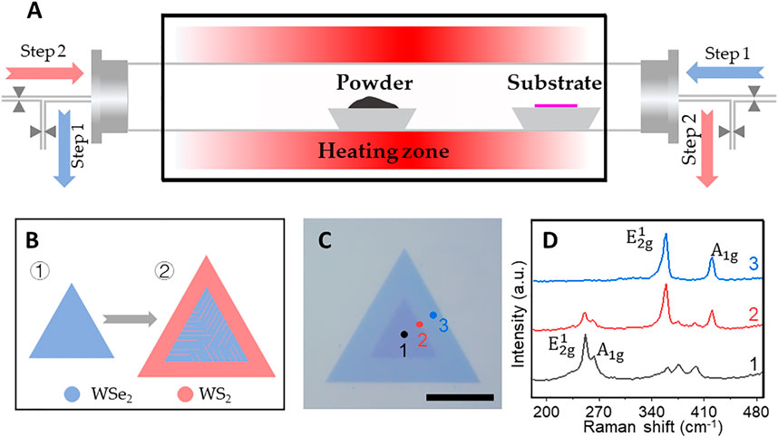
FIGURE 1. CVD synthesis strategy for monolayer WSe2 growth and WS2 epitaxial growth. (A) Diagrammatic sketch of the single supply source CVD growth method with controllable airflow directions. (B) Diagrammatic sketch of the WSe2/WS2 2D quantum well superlattice synthesis strategy. (C) Optical image of the WSe2/WS2 lateral heterojunction using the reverse airflow method; scale bar is 10 μm. (D) Raman spectra corresponding to the three points marked in Figure 1.
2.2 Growth of WSe2/WS2 2D quantum well superlattices
To obtain the WSe2/WS2 2D quantum well, the monolayer WSe2 was chosen as a seed to further the epitaxial growth of the monolayer WS2. At the same time, quantum wells started forming at the interfaces of WSe2/WS2 lateral heterojunctions. For the epitaxial growth of WS2, the WS2 powder and prepared monolayer WSe2 (substituted for clean substrate and WSe2 powder) were placed at the same position in another specified CVD system similar to the system used for WSe2 growth. Likewise, during the period of temperature increase, the growth substrate was placed upstream of the source and the airflow (along the “step 1” arrow in Figure 1A) was set to 300 sccm for 15 min, and then reduced to 100 sccm and kept at that airflow rate. When the central heating zone reached the target temperature of 1120°C, the airflow was set to 100 sccm in the transferred direction (along the “step 2” arrow in Figure 1A), ensuring the growth substrate was located downstream of the source, and then maintained for 5 min for WS2 epitaxial growth. After that, the airflow direction was reversed (along the “step 1” arrow in Figure 1A) to stop the epitaxial growth process and allow it to naturally cool down to room temperature. The entire process occurred under ambient pressure in an argon atmosphere.
2.3 Characterization
Optical microscopy and STEM were used to characterize the morphologies of the nano-heterojunctions. The Raman spectra were performed using a Renishaw confocal Raman system excited by a 488-nm laser at room temperature. The applied laser power was set to 5%, and the exposure time was approximately 0.1 s. STEM imaging and EELS analysis were carried out using a Thermo Scientific Themis Z 3.2 system equipped with a cold field-emission gun and a mirror lens corrector operating at 300 kV. All STEM experiments were completed at room temperature. The strain distribution of the nanostructure was calculated based on the geometric phase analysis method using the FRWRtools plugin for DigitalMicrograph (www.physik.hu-berlin.de/en/sem/software/software_frwrtools).
The STEM samples were prepared using a poly-methyl-methacrylate (PMMA)–assisted method. PMMA was spin-coated onto the heterojunction sample until the PMMA layer fully covered the heterojunction sample and then baked at 180°C for 3 min. Afterward, the wafer was immersed in a saturated 0.2 M NaOH solution to etch the SiO2 layer. After the sample coated with PMMA was separated from the silicon wafer, it was transferred into fresh deionized water, repeatedly, to wash away residual contaminants and then fished by a conventional lacey carbon film TEM grid. The as-transferred sample was dried naturally in the ambient environment and then immersed in acetone overnight to clean up the PMMA coating layers. All the STEM samples were baked at 150°C for 6 h to avert unexpected contamination from hydrocarbon.
3 Results and discussion
3.1 Lateral heterojunction with 2D quantum wells
Figure 1B is the synthesis strategy diagrammatic sketch of the WSe2/WS2 2D quantum well, and Figure 1B① and Figure 1B② show the idealized schematic sketch of the monolayer WSe2 and the WSe2/WS2 2D quantum well, respectively. The WS2 quantum well was inserted into the monolayer WSe2, which started to grow from the WSe2/WS2 interface, as depicted in Figure 1B②. The width of the quantum well in Figure 1B② is exaggerated to make the display easy to recognize and understand. Figure 1C is the optical image of the monolayer WSe2/WS2 lateral heterojunction synthesized on a silica/silicon substrate; it shows two concentric regions with slightly different optical contrast due to the refractive index and thickness difference between tungsten selenide and tungsten sulfide (Henrie et al., 2004; Blake et al., 2007). Here, the nanoscale WS2 2D quantum wells formed at the WSe2/WS2 interface but were difficult to recognize in the optical image due to the low enlargement factor of optical microscopy. To further explore the spatial modulation of structural and optical properties in WSe2/WS2 lateral heterostructures, the confocal Raman microscope was used to characterize the nanostructure. We picked up three points marked ''1,″ ''2,″ and ''3″ in Figure 1C for the Raman study, where ''1'' (black point), ''2'' (red point), and ''3'' (blue point) are located at the internal tungsten selenium, the WSe2/WS2 interface, and the epitaxial tungsten sulfide area, respectively. The Raman spectra at different locations showed distinct differences: the internal region Raman spectrum had a significant peak at 250 cm−1 (black line in Figure 1D), consistent with the A1g resonance pattern of WSe2, and the peripheral region Raman spectrum had two significant peaks, at 350 cm−1 and 419 cm−1 (blue line in Figure 1D), corresponding to the E12g and A1g resonance patterns of WS2. Significantly, the Raman spectrum of the WSe2/WS2 interface showed both the resonance modes of WSe2 and the resonance modes of WS2 (red line in Figure 1D), which indicate that tungsten selenium and tungsten sulfide coexist well within the same triangular domain.
3.2 Strain analysis in a WSe2/WS2 2D quantum well
These WS2 quantum wells extending from the WSe2/WS2 interface, mostly distributed in parallel, were generally observed in the lateral WSe2/WS2 heterojunction samples, as shown in the STEM image in Figure 2A. Figure 2B is the enlarged view of Figure 2A, and the clear boundaries between WSe2 and WS2 in the WSe2/WS2 2D quantum well are apparent. Also, the strain distribution corresponding to Figure 2B is given in Figure 2C. The perfect lattice from the monolayer WSe2 was used as a reference for calculating the strain. In the perfect monolayer, the lattice constant of WSe2 was ∼4% larger than that of WS2, which indicates that the WS2 quantum well had high and uniform tensile strain along its growth direction, leading to the observed dislocation-free transverse interface. However, the situation was different in the direction perpendicular to the growth direction, where there was a comparatively larger lattice mismatch between WS2 and WSe2 (∼4.3 ± 0.5%), as revealed by the calculated strain distribution spectrum.
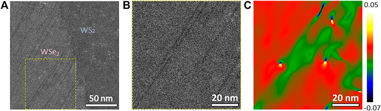
FIGURE 2. Strain analysis of WS2 2D quantum wells at the interface between WSe2 and WS2. (A) STEM image of WS2 quantum wells with uniform width at the WSe2/WS2 lateral heterojunction interface. (B) Enlarged view of (A). (C) Corresponding strain distribution of (B).
3.3 Atomic-scale sharp WS2 2D quantum well
Figure 3A shows a 2D quantum well in which the monolayer of the WS2 nanoribbons is laterally sandwiched between two monolayer WSe2 nanoribbons. As shown in the STEM image in Figure 3A, the Se and S atomic sites are distinguished from the image contrast due to different atomic numbers (Krivanek et al., 2010; Zhou et al., 2012), where the WS2 quantum well shows a lower image intensity than the surrounding monolayer WSe2, and the WS2/WSe2 interface is marked by red dashed lines.
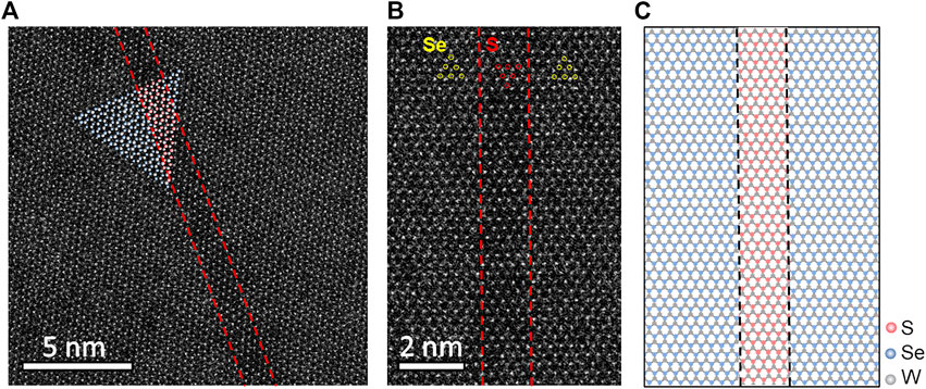
FIGURE 3. Atomic-scale sharp WS2 2D quantum well embedded in monolayer WSe2. (A) STEM image of the WSe2/WS2 lateral heterojunction interface; the red dashed line highlights the interface between WSe2 and WS2. (B) High-resolution STEM-ADF image of a WS2 quantum well; the red dashed line along the armchair orientation highlights the interface between WSe2 and WS2. The yellow and red circles mark the Se and S atoms, respectively. (C) Atomic structural model of the WS2 quantum well corresponding to (B). Pink, blue, and gray spheres represent the S, Se, and W atoms, respectively.
The high-resolution STEM-annular dark-field (ADF) image of a WS2 quantum well is shown in Figure 3B; the yellow and red circles mark Se and S atoms, respectively. It was observed that the ∼1.2 nm WS2 quantum well was embedded in a single layer of WSe2 and growing along the hexagonal armchair orientation. Correspondingly, Figure 3C is the idealized atomic structural model of the WS2 quantum well according to Figure 3B. The interface is highlighted by the red and black dashed lines in Figures 3B,C, respectively. It is obvious that there are no mismatches or defects at the interface, which means a fully coherent lateral interface was formed.
3.4 Formation mechanism of WS2 quantum wells at the WSe2/WS2 lateral interface
Similar to film growth, strain relaxation at the epitaxial interface with intrinsic lattice mismatch produces mismatch dislocation once the critical width is exceeded (Matthews and Blakeslee, 1974; Jain et al., 1997). For the lateral WSe2/WS2 heterostructures, the mismatch dislocation array spaced ∼8 nm in the zigzag orientation was expected to alleviate the lattice strain due to the presence of ∼4% lattice mismatch between WSe2 and WS2. Through careful observation, it was found that WS2 quantum wells relied on a dislocation core for growth at the lateral WSe2/WS2 heterointerface in general, and further growth was considered driven by misfit dislocation climb. As shown in Figure 4A, the insertion of one W atom and two S atoms from the gas source was considered initiation of the dislocation-driven growth as such dislocation drove the W and S atoms to invade the WSe2 along the hexagonal zigzag orientation, which is consistent with our experimental results. According to statistical analysis, the width of WS2 quantum wells is about 1.2 nm, which is equivalent to the width of the four WS2 unit cells. A four-unit-cell-width and a one-unit-cell-width WS2 nano-seed, shaded in light red in Figure 4B,are shown penetrating to the WSe2 monolayer to propagate the quantum well.
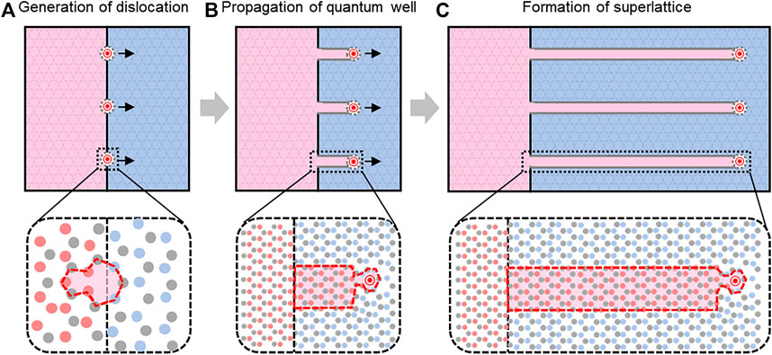
FIGURE 4. Diagrammatic sketch of the formation mechanism of WS2 quantum wells at the interface between WSe2 and WS2.(A) Generation of dislocation. (B) Propagation of quantum wells. (C) Formation of the WS2 superlattice.
Theoretically, the formation of the mismatch dislocation at the interface was required per each ∼8 nm interval to release strain. After repeating the aforementioned growth mechanism, parallel WS2 quantum wells were formed, and these parallel 2D narrow nano-bands were quantum well superlattices, as shown in Figure 4C.
3.5 Promising 2D quantum well superlattices with atomically sharp lateral interfaces
According to the aforementioned results, there is potential to generate a 2D quantum superlattice, consisting of equally spaced 2D quantum wells, if growth conditions are precisely controlled. The WS2 quantum well grown by this mechanism formed a type II band arrangement with the surrounding monolayer WSe2, as shown in Figure 4B.
Meanwhile, the n-type doped ultranarrow WS2 nanoribbons were expected to be conductors due to the type II band alignment. Nanoribbons of higher carrier concentrations can be obtained by this process of modulation doping as ionizing donors are distributed in the WSe2 region and thus reduce Coulomb scattering in WS2. Furthermore, the quantum wells shown in Figure 5A are not evenly spaced, and such a phenomenon could be attributed to the periodic array that was not initially formed at the interface. The bottom area in Figure 5B is an enlarged display of the red dotted frame in Figure 5A. There are different energy band distributions in the region of tungsten sulfide and tungsten selenide. From Figure 5A and Figure 5B, it can be concluded that the length distribution of quantum wells ranges from ten nanometers to a few microns, while the spacing between the quantum wells is about 8 nm, which is basically consistent with the previous theoretical analysis results. High-quality 2D semiconductor quantum well superlattices may be prepared by a misalignment drive mechanism if the growth parameters of the chemical vapor deposition (CVD) system are stably controlled.
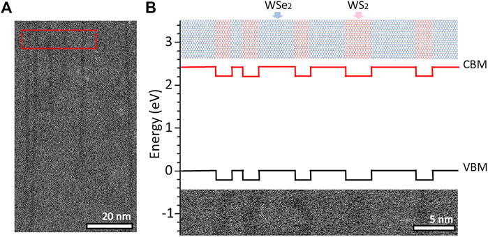
FIGURE 5. WS2 quantum superlattice. (A,B) Atomic structure model of the WSe2/WS2 superlattice and the calculated band structure. The red and black solid lines represent the valence band maximum (VBM) and the conduction band minimum (CBM), respectively.
4 Conclusion
To summarize, we successfully synthesized sub-2-nm quantum well arrays in WSe2/WS2 lateral heterojunctions. High-resolution STEM images showed the atomically sharp lateral interfaces between the WS2 quantum well and monolayer WSe2. Among them, ∼4% lattice mismatch between WSe2 and WS2 monolayers led to misfit dislocation arrays with an average spacing of 8 nm at the lateral heterointerface. After that, dislocations drove the corresponding atoms to penetrate along the hexagonal armchair orientation, which plays a key role in the efficient growth of quantum wells. According to the results of the WSe2/WS2 lateral heterojunction system, such quantum well superlattice structures are expected to be formed in varied lateral heterojunctions. Considering the large variety of 2D materials, 2D quantum well superlattices in varied lateral heterojunctions will display abundant photonic electronic properties, which provide new roads for the study of topological insulators and superconductors.
Data availability statement
The original contributions presented in the study are included in the article/Supplementary Material; further inquiries can be directed to the corresponding author.
Author contributions
HY: conceptualization, methodology, formal analysis, resources, visualization, and writing—original draft. LZ: methodology and formal analysis. ZH: conceptualization and visualization. TZ: methodology, and writing—review and editing. SZ: investigation, validation, and formal analysis. XZ: laboratory resources. ZA: investigation. XL: visualization. BZ: conceptualization, writing—review and editing, supervision, and project administration. All authors have read and agreed to the published version of the manuscript.
Funding
This work was supported by the Natural Science Foundation of Changsha (Grant. kq2202092).
Conflict of interest
The authors declare that the research was conducted in the absence of any commercial or financial relationships that could be construed as a potential conflict of interest.
The Reviewer, EZ, declared a shared affiliation with the author, BP, at the time of the review.
Publisher’s note
All claims expressed in this article are solely those of the authors and do not necessarily represent those of their affiliated organizations, or those of the publisher, the editors, and the reviewers. Any product that may be evaluated in this article, or claim that may be made by its manufacturer, is not guaranteed or endorsed by the publisher.
Supplementary material
The Supplementary Material for this article can be found online at: https://www.frontiersin.org/articles/10.3389/fmats.2023.1108077/full#supplementary-material
References
Blake, P., Novoselov, K. S., Neto, A., Jiang, D., Yang, R., Booth, T. J., et al. (2007). Making graphene visible. Appl. Phys. Lett. 91, 063124. doi:10.1063/1.2768624
Chen, P., Zhang, Z., Duan, X., and Duan, X. (2018). Chemical synthesis of two-dimensional atomic crystals, heterostructures and superlattices. Chem. Soc. Rev. 47, 3129–3151. doi:10.1039/c7cs00887b
Faist, J., Capasso, F., Sivco, D. L., Sirtori, C., Hutchinson, A. L., and Cho, A. Y. (1994). Quantum cascade laser. Science 264, 553–556. doi:10.1126/science.264.5158.553
Geim, A. K., and Grigorieva, I. V. (2013). Van der Waals heterostructures. Nature 499, 419–425. doi:10.1038/nature12385
Gong, Y., Lei, S., Ye, G., Li, B., He, Y., Keyshar, K., et al. (2015). Two-step growth of two-dimensional WSe2/MoSe2 heterostructures. Nano Lett. 15, 6135–6141. doi:10.1021/acs.nanolett.5b02423
Gudiksen, M. S., Lauhon, L. J., Wang, J., Smith, D. C., and Lieber, C. M. (2002). Growth of nanowire superlattice structures for nanoscale photonics and electronics. Nature 415, 617–620. doi:10.1038/415617a
Han, Y., Li, M. Y., Jung, G. S., Marsalis, M. A., Qin, Z., Buehler, M. J., et al. (2018). Sub-nanometre channels embedded in two-dimensional materials. Nat. Mater 17, 129–133. doi:10.1038/nmat5038
Henrie, J., Spencer, K., Schultz, S. M., and Hawkins, A. (2004). Electronic color charts for dielectric films on silicon. Opt. Express 12, 1464–1469. doi:10.1364/opex.12.001464
Jain, S. C., Harker, A. H., and Cowley, R. A. (1997). Misfit strain and misfit dislocations in lattice mismatched epitaxial layers and other systems. Philos. Mag. A 75, 1461–1515. doi:10.1080/01418619708223740
Krivanek, O. L., Chisholm, M. F., Nicolosi, V., Pennycook, T. J., Corbin, G. J., Dellby, N., et al. (2010). Atom-by-atom structural and chemical analysis by annular dark-field electron microscopy. Nature 464, 571–574. doi:10.1038/nature08879
Li, M.-Y., Shi, Y., Cheng, C.-C., Lu, L. S., Lin, Y. C., Tang, H. L., et al. (2015). Epitaxial growth of a monolayer WSe2-MoS2 lateral p-n junction with an atomically sharp interface. Science 349, 524–528. doi:10.1126/science.aab4097
Liu, L., Park, J., Siegel, D. A., McCarty, K. F., Clark, K. W., Deng, W., et al. (2014). Heteroepitaxial growth of two-dimensional hexagonal boron nitride templated by graphene edges. Science 343, 163–167. doi:10.1126/science.1246137
Liu, Y., Huang, Y., and Duan, X. (2019). Van der Waals integration before and beyond two-dimensional materials. Nature 567, 323–333. doi:10.1038/s41586-019-1013-x
Liu, Z., Ma, L., Shi, G., Zhou, W., Gong, Y., Lei, S., et al. (2015). In-plane heterostructures of graphene and hexagonal boron nitride with controlled domain sizes. Nat. Nanotech 8, 119–124. doi:10.1038/nnano.2012.256
Matthews, J. W., and Blakeslee, A. E. (1974). Defects in epitaxial multilayers. I. Misfit dislocations. J. Cryst. Growth 27, 118–125. doi:10.1016/0022-0248(74)90424-2
Shi, E., Yuan, B., Shiring, S. B., Gao, Y., Akriti, , Guo, Y., et al. (2020). Two-dimensional halide perovskite lateral epitaxial heterostructures. Nature 580, 614–620. doi:10.1038/s41586-020-2219-7
Zhang, K., Ding, C., Pan, B., Wu, Z., Marga, A., Zhang, L., et al. (2021). Visualizing van der Waals epitaxial growth of 2D heterostructures. Adv. Mat. 33, 2105079. doi:10.1002/adma.202105079
Zhang, Z., Chen, P., Duan, X., Zang, K., Luo, J., and Duan, X. (2017). Robust epitaxial growth of two-dimensional heterostructures, multiheterostructures, and superlattices. Science 357, 788–792. doi:10.1126/science.aan6814
Zhou, W., Oxley, M. P., Lupini, A. R., Krivanek, O. L., Pennycook, S. J., and Idrobo, J.-C. (2012). Single atom microscopy. Microsc. Microanal. 18, 1342–1354. doi:10.1017/s1431927612013335
Keywords: chemical vapor deposition (CVD), lateral epitaxial growth, monolayer WSe2, 2D quantum well superlattices, misfit dislocation-driven growth
Citation: Yang H, Zeng L, Huang Z, Zhang T, Zhang S, Zhang X, Ao Z, Lan X and Zhang B (2023) Dislocation-driven growth of WS2/WSe2 quantum well superlattices. Front. Mater. 10:1108077. doi: 10.3389/fmats.2023.1108077
Received: 25 November 2022; Accepted: 15 February 2023;
Published: 02 March 2023.
Edited by:
Enbo Zhu, University of California, Los Angeles, United StatesReviewed by:
Du Xiang, Fudan University, ChinaYingqiu Zhou, Technical University of Denmark, Denmark
Huifang Ma, Nanjing Tech University, China
Bosi Peng, University of California, Los Angeles, United States
Copyright © 2023 Yang, Zeng, Huang, Zhang, Zhang, Zhang, Ao, Lan and Zhang. This is an open-access article distributed under the terms of the Creative Commons Attribution License (CC BY). The use, distribution or reproduction in other forums is permitted, provided the original author(s) and the copyright owner(s) are credited and that the original publication in this journal is cited, in accordance with accepted academic practice. No use, distribution or reproduction is permitted which does not comply with these terms.
*Correspondence: Baihui Zhang, Ymh6aGFuZ0Bjc3UuZWR1LmNu