 Darpan Mishra
 Ramesh Kumar Sonkar
- 1Tyndall National Institute, University College Cork, Cork, Ireland
- 2Department of Electronics and Electrical Engineering, Indian Institute of Technology Guwahati, Guwahati, Assam, India
On-chip integrated optical phase shifters are an important part of optical phase modulators. The performance of such modulators relies heavily on the phase shifter performance, which in turn depends on multiple process parameters. This paper reports the study of the effect of different process parameters on the performance of a silicon PN optical phase shifter obtained by process simulation using Silvaco® TCAD. The effect of dopant implantation dose, implantation energy, annealing temperature and time, wafer temperature, wafer tilt and rotation, and pre-amorphization on the phase and absorption of light is discussed. The 3-dB modulation bandwidth of a lumped phase shifter and the dependency of the performance metrics on different process parameters are presented. Monte Carlo numerical simulation shows that the free-carrier absorption has a much greater dependency on the process parameters than the phase shift. The study shows that ion channeling poses a limiting factor on the phase shifter performance, which can be improved by tilting the wafer or using a pre-amorphized substrate for implantation. The study shows that the 3-dB modulation bandwidth is highly dependent on the wafer tilt angle, rotation angle, and the lattice structure of the solid substrate. A bandwidth improvement of more than 5× is observed with 1.7× lower absorption for a pre-amorphized sample at −5 V compared to a crystalline sample with the same process flow.
1 Introduction
It is estimated that the photonic integrated circuit (PIC) industry will see a compound annual growth rate (CAGR) of 28.30% during 2020–2025 [1]. Compared to the traditional electronic integrated circuits (EICs), PICs are fast, have higher bandwidth, and are energy efficient. Silicon photonics is a vastly growing area with applications in medical [2], astronomy [3], communication [4], etc. The global silicon photonics market is expected to expand at a CAGR of 29.61% and is estimated to reach USD 4918.87 million by 2027. [5]. The rapid rate of increase in data traffic requires low-cost, high-bandwidth devices where silicon photonics provides a viable solution. Optical modulators modulate data that are sent via photons through a fiber. The silicon PN modulators are fast, and modulation occurs through the use of phase shifters using the free-carrier plasma dispersion (FCPD) effect [6]; [7]. The modulator characteristics are highly dependent on the phase shifter metrics, which are the phase shift, loss, and bandwidth. The two commonly used modulator structures, viz., the Mach-Zehnder and ring/racetrack modulators have been widely investigated and huge amount of literatures are present [8]; [9,10]; [11]; [12]; [13,14]. Different driving configurations and architectures [15]; [16]; [17] have been investigated to realize modulators with large modulation bandwidth, low energy-per-bit transmission, low bit-error-rate, and high extinction ratio.
Studies can be found in literature where different materials have been integrated in silicon platform to improve the device performance like electro-optic polymer [18], barium titanate [19], indium tin oxide [20] etc. However, such heterogenous integration techniques seldom resolves the trade-offs involved and results in design and fabrication complexity. Multiple studies can be found in literature where silicon optical phase shifter performance is optimized by adjusting the process parameters. A study of ion implantation condition on PN phase shifter performance can be found in [21] which took into account the effect of tilt angle and implantation energy. A U-shaped [22], and S-shaped [23] PN junction has been reported with enhanced performance by optimizing the implantation energy, dose, and tilt angle. The effect of P and N doping on the phase shift and absorption loss is reported in [24] along with the effect of the PN junction offset. However, all these studies focussed on a limited number of process parameters, and a thorough study, including the tradeoffs between phase shift, loss, and bandwidth, have not yet been reported so far to the best of the authors’ knowledge.
The phase shifter performance depends on the fabrication process flow and can be tuned by tuning the process parameters accordingly. Multiple tradeoffs are involved, and the effect of different parameters needs to be taken into consideration. Changing the process parameter values changes the phase shift, loss, series resistance, and junction capacitance. Designing a phase shifter with higher phase shift and lower loss may result in lower modulation bandwidth despite having a smaller size. Therefore, it is important to study the degree of dependency of the performance metrics on different process parameters and to tune them accordingly. Virtual fabrication ensures fabrication-ready design by incorporating practical effects in the design steps. Process simulation is a virtual fabrication tool that takes the effect of different fabrication parameters into the device design. This ensures that the device performance upon fabrication is close to the simulated results. Process simulation allows the flexibility of tuning multiple parameters to enhance the device performance. Over the years, multiple models and tools have been developed to accurately predict dopant implantation, diffusion, annealing, damage accumulation, etc. [25]; [26]; [27]; [28]; [29]. These constitutes the technology computer-aided design (TCAD) simulation of different electronic and optoelectronic devices. Multiple studies have been done using TCAD tools to optimize and design different devices and technologies [30]; [31]; [32]; [33].
In this paper, TCAD simulation is done to study the effect of different process parameters like wafer temperature, implantation dose, implantation energy, wafer tilt, wafer rotation, annealing temperature and time, and pre-amorphization on a silicon optical PN phase shifter performance. Process simulation, as well as device simulation, is carried out and the effect of each parameter on the phase shift, free-carrier absorption (FCA), and the 3-dB modulation bandwidth is presented and discussed. A reference PN phase shifter is designed, and the effect of different parameters on the performance is quantified by comparing with the reference phase shifter. The PN phase shifter process steps, structure, and metrics are given in Section 2. Section 3 presents the process parameter study, and Section 4 gives a comparison and discussion of the effect of different process parameters on the phase shifter performance. Section 5 concludes the paper. A supplementary file is provided with this manuscript, which gives the effect of different process parameters on the phase shifter resistance and capacitance. The study presented in this manuscript focuses on how different parameters affect the optical PN phase shifter performance at the process level and identify the limiting factors to realize an efficient phase shifter by tuning the process parameters accordingly. Designing and optimizing the modulator performance that includes a different set of performance metrics is beyond the scope of this study.
2 Phase shifter simulation
A 220 nm silicon-on-insulator (SOI) wafer with 2 μm buried oxide (BOX) and 500 μm bottom silicon is used in this study. The SOI wafer orientation used in this paper is shown in Figure 1 with the different crystallographic directions. A <100> intrinsic crystal is used with wafer flat along [01
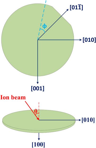
FIGURE 1. (A) Top-view and (B) side-view of SOI wafer depicting orientation and different crystallographic axes used in this paper.
When dopants are implanted, the collision between the dopant atoms and host (silicon) atoms leads to lattice damage [28]. Dopants that rest in interstitial sites are inactive and need to substitute the bonded silicon atom sites to be electrically active and contribute to electrical conduction. To recrystallize and activate the dopants, annealing is done whereby the wafer is subjected to high temperature for a short duration of time [34]. The annealing step provides energy to the dopant atoms/ions and leads to the broadening of the as-implanted profile due to diffusion. In this study, Monte Carlo analysis is used with the ion implantation being modeled by the binary collision approximation (BCA) [35]; [36]. During annealing, different regions having different dopant and defect concentrations recrystallize leading to dopant-interstitial and dopant-vacancy pair creation. The analysis of defect cluster formation is important for devices used in high-speed applications [28]; [37].
The effect of different parameters on phase shifter performance is quantified by comparing it with a reference phase shifter. The wafer orientation for the reference phase shifter is same as shown in Figure 1 with θ = 0 and ϕ = 0. The PN junction is formed by single implantation of boron and phosphorus with a dose of 2 × 1013 cm−3 each, which is below the amorphization threshold [26]. The implantation energy is selected to be 17 keV and 25 keV for boron and phosphorus, respectively. The wafer is kept at room temperature (20 °C), and the beam divergence is 1°. To form the rib structure, a 120 nm anisotropic etch is performed, keeping the waveguide width 500 nm. To form the anode and cathode, highly doped P++ and N++ regions are formed to ensure ohmic contacts. The P++ and N++ regions are formed with an implantation dose of 1 × 1015 cm−2 using boron and phosphorus with the energy of 3 keV and 10 keV, respectively. Each of the implantation steps is followed by rapid thermal annealing (RTA) at 1,100 °C for 10 s in a nitrogen ambient. The top cladding is formed by depositing 2 μm silicon dioxide. Vias are created over the P++ and N++ regions, followed by the deposition of aluminum to form the anode and cathode, respectively. The PN phase shifter structure is shown in Figure 2.
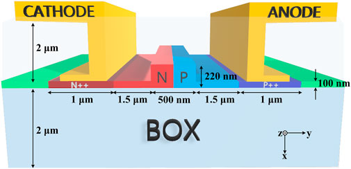
FIGURE 2. 3D front view of the silicon phase shifter (not to scale).
The PN phase shifter is operated in reverse bias with carrier depletion leading to a change in the refractive index. The change in the carrier concentration changes the refractive index and the FCA, which is given by Soref for 1,550 nm wavelength as [6]; [38].
Where Δn and Δα are the changes in the refractive index and FCA coefficient, respectively. ΔNe (ΔNh) is the change in the electron (hole) concentration with applied reverse bias voltage.
The change in the mode effective index (Δneff) is given as [21]
where E is the mode electric field distribution.
The phase shift (Δφ) and FCA (α) can be calculated as
Where L is the phase shifter length and λ0 is the free-space wavelength of light. The phase shifter is also characterized by the modulation efficiency, which is the product of voltage and phase shifter length required to obtain π phase shift, and is calculated as
A lower value of the modulation efficiency corresponds to a better phase shifter. The phase shifter simulation and different parameter study is done using Silvaco® TCAD. Silvaco® Athena has been used for process simulation and Silvaco® Atlas for the device simulation. The phase shifter performance is analyzed for the 1,550 nm wavelength of operation. The small-signal analysis is done by extracting the admittance matrix at 50 GHz frequency. The frequency normalized impedance is calculated, and the 3-dB bandwidth is determined for a 50 Ω source and termination impedance when the phase shifter is driven as a lumped element [39]. The 3 dB bandwidth (f) is determined as
where Cd is the PN depletion capacitance and R is the equivalent resistance by taking into account the source, termination, and the series PN resistance. A phase shifter with lower junction depletion capacitance and series resistance leads to higher modulation bandwidth. The reference phase shifter has a phase shift of 42° and FCA of 1.54 dB for a 1 mm long phase shifter at -5 V. The phase shifter modulation efficiency is 2.14 V cm with a 3-dB bandwidth of 7.15 GHz at -5 V.
3 Parameter study
This section presents the effect of different process parameters on the phase shifter performance, namely, phase shift, absorption, and the 3 dB bandwidth as obtained using Silvaco® TCAD. The process parameters include the implantation dose, implantation energy, annealing temperature and time, wafer temperature, wafer tilt, wafer rotation, and substrate pre-amorphization. Performance comparison with different process parameters has been made with the reference phase shifter to analyze and quantify the performance dependency on different parameters. In each of the parameter studies, only one parameter is changed, keeping all other parameters same as that of the reference phase shifter unless otherwise specified. The phase, absorption, and bandwidth for different parameter variations are shown in this paper. The phase shifter resistivity and capacitance curves are given in the supplementary file of this paper.
3.1 Implantation dose
Changing the implantation dose, changes the waveguide dopant concentration. The implantation profile is a Gaussian-like shape that broadens upon annealing. Same implantation doses of boron and phosphorus have been used to form the PN junction. The effect of three different implantation doses are evaluated, keeping the boron and phosphorus dose same in each case. The phase shift and FCA per unit length with three different implantation doses, viz., 1 × 1013 cm−2, 2 × 1013 cm−2 (reference), and 3 × 1013 cm−2 are shown in Figures 3A, B respectively. Increasing the dose increases the electron and hole carrier concentration, thereby increasing both the phase shift and absorption loss. Comparison between an implantation dose of 1 × 1013 cm−2 and 3 × 1013 cm−2 shows that for 3× increase in dose, the phase shift and absorption increases by 1.39× and 2.96× respectively at -5 V. The phase shifter resistance and capacitance is given in the Supplementary Figure S1 respectively. The 3-dB bandwidth for different implantation doses are shown in Figure 3C. The bandwidth change is negligible with the change in the implantation dose. The bandwidth increases to 7.6 GHz for a dose of 3 × 1013 cm−2. The bandwidth improvement is only ∼6.3% compared to the reference phase shifter at 5 V reverse bias.
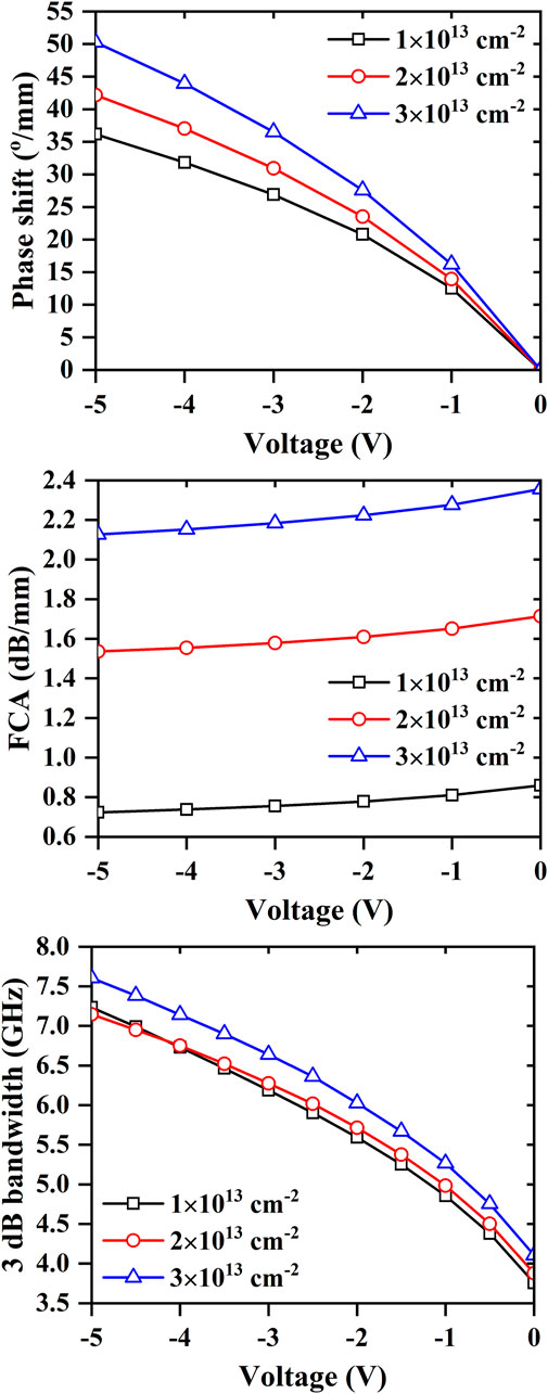
FIGURE 3. (A) Phase shift per unit length, (B) free-carrier absorption per unit length, and (C) 3-dB bandwidth for different implantation doses. The boron and phosphorus implantation dose is equal for each sample.
3.2 Implantation energy
Changing the implantation energy changes the peak position of the implantation profile. The implantation energy of both boron and phosphorus is changed by ± 3 keV from that of the reference phase shifter. The phase shift and FCA loss per unit length for different implantation energies is shown in Figures 4A, B respectively. The figure legend shows the “boron energy/phosphorus energy”. Three different samples with different boron/phosphorus energies, viz., 14 keV/22 keV, 17 keV/25 keV (reference), and 20 keV/28 keV, have been simulated. Similar phase shifts are observed for all three samples. However, the absorption loss of the three samples is different, with the highest absorption occurring for the reference phase shifter. The lowest absorption is for the 20 keV/28 keV implantation energy and is 1.18× lower than the reference phase shifter. The absorption depends on the modal overlap of free electrons and holes. For the reference phase shifter, the carrier concentration at the mode maxima is larger than for the other two samples. Supplementary Figure S2 of the supplementary file shows the phase shifter resistivity and capacitance curves. The phase shifter bandwidth is shown in Figure 4C, from which it can be observed that the bandwidth decreases to 6.84 GHz for the lowest implantation energy.
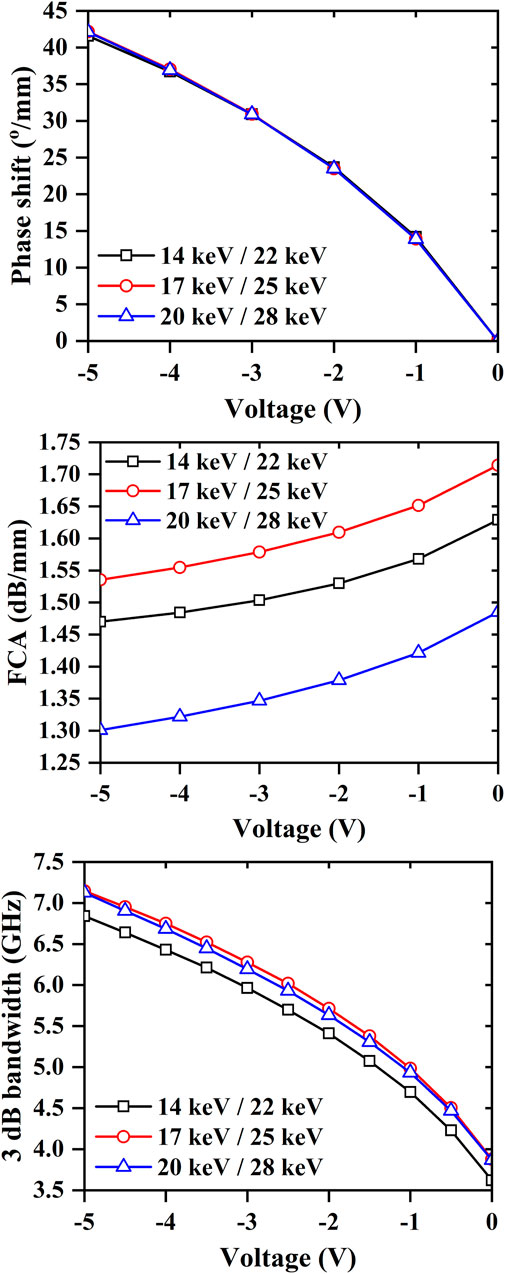
FIGURE 4. (A) Phase shift per unit length, (B) free-carrier absorption per unit length, and (C) 3-dB bandwidth for different boron/phosphorus implantation energies.
3.3 Annealing temperature and time
As discussed previously, annealing is required for wafer recrystallization and dopant activation. Annealing at different temperatures for different times leads to different doping and damage concentration profile. Also, as-implanted profile broadening takes place during annealing by damage and dopant diffusion [40]. Four different annealing conditions have been evaluated: 800 °C for 180 s, 900 °C for 90 s, 1,000 °C for 30 s, and 1,100 °C for 10 s (reference). The phase shift and FCA per unit length curve for the different annealing conditions are shown in Figures 5A, B respectively. The effect of different annealing temperature and time on the phase shift is negligible. However, compared to the reference phase shifter, lower temperature, longer duration annealing leads to 1.12× lower absorption loss. The phase shifter resistivity and capacitance of all the samples are shown in Supplementary Figure S3 of the supplementary file. Figure 5C shows the 3-dB bandwidth of all four samples. It is observed that the bandwidth improves as the annealing temperature decreases and the duration increases. An improvement of ∼8% has been observed for the sample annealed at 800 °C for 3 min compared to the reference sample.
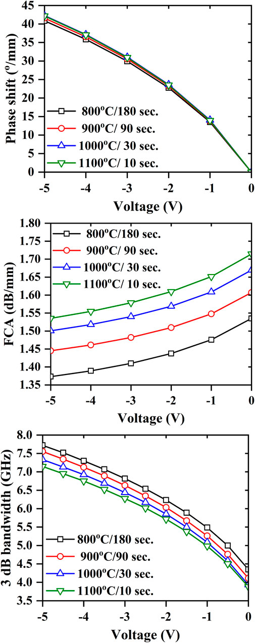
FIGURE 5. (A) Phase shift per unit length, (B) free-carrier absorption per unit length, and (C) 3-dB bandwidth for different annealing temperature/time.
3.4 Wafer temperature
Dopant implantation on a heated sample results in a broadened as-implanted doping profile due to dopant diffusion. The wafer temperature is varied from 20 °C (room temperature) to 150 °C and 300 °C. The phase shift and FCA loss per unit length are shown in Figures 6A, B respectively for different wafer temperatures. Increasing the wafer temperature increases the absorption loss with negligible change in the phase shift. An increase of 7.1% in absorption loss is observed at -5 V when the wafer temperature is changed from 20 °C (reference) to 300 °C. Supplementary Figure S4 in the supplementary file presents the phase shifter resistivity and capacitance curves for different wafer temperatures. The phase shifter bandwidth for the three samples are shown in Figure 6C. The bandwidth decreases with an increase in temperature. A 4% decrease in bandwidth at -5 V is observed for 300 °C heated wafer compared to the wafer at room temperature.
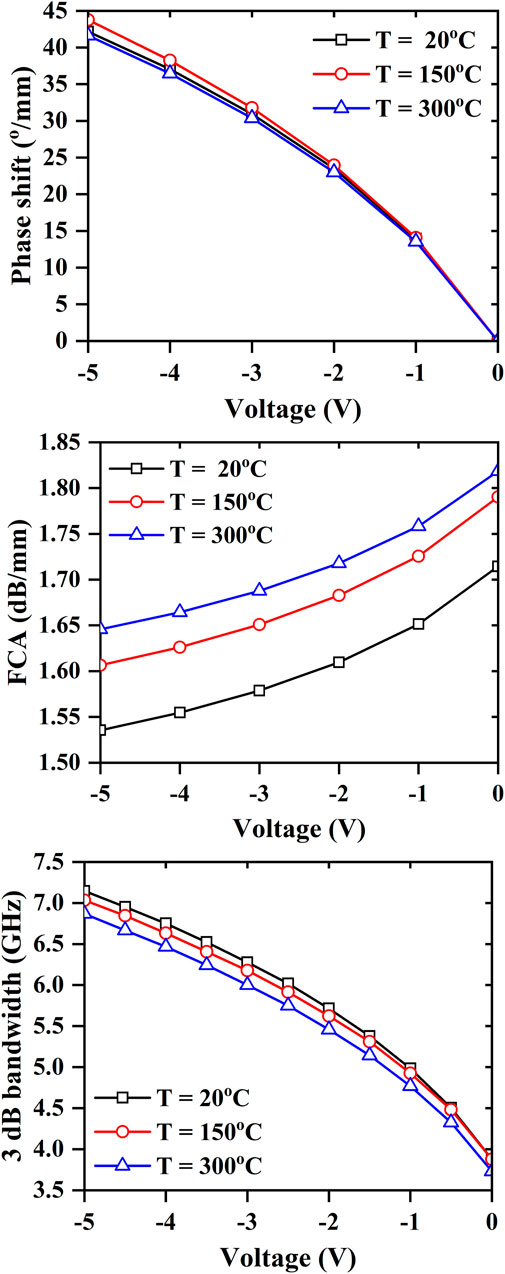
FIGURE 6. (A) Phase shift per unit length, (B) free-carrier absorption per unit length, and (C) 3-dB bandwidth for different wafer temperatures.
3.5 Wafer tilt
The lattice structure plays an important role in the channeling of dopant atoms or ions [41]. As dopants are implanted, the ions travel through the crystallographic planes. Different planes have different atomic density, due to which the degree of ion channeling is different in different directions. If a particular crystallographic axis provides larger ease of ion travel, the as-implanted profile is broadened with a lower concentration Gaussian peak. For an ion beam perpendicular to the <100> wafer surface, the ion channeling is more. As the wafer is tilted, ion channeling reduces, thereby leading to less profile broadening and higher peak concentration. The wafer tilt (θ) is varied from 1° to 9° in steps of 2°, and its effect on the phase shifter performance is evaluated. Large variation in phase shift as well as absorption loss per unit length can be seen in Figures 7A, B for different tilt angles. The phase shift is
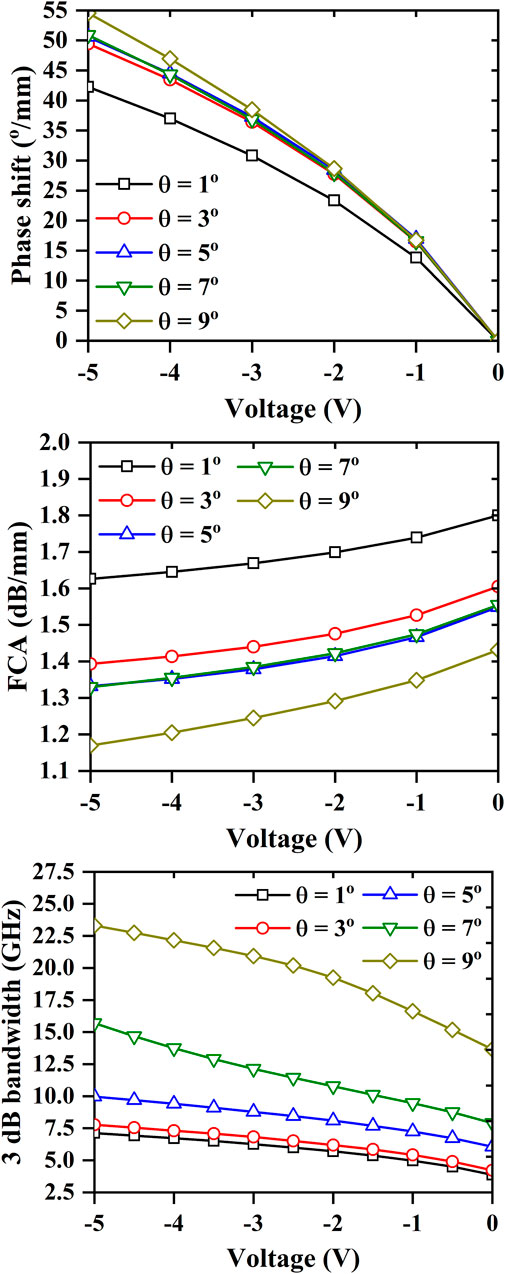
FIGURE 7. (A) Phase shift per unit length, (B) free-carrier absorption per unit length, and (C) 3-dB bandwidth for different wafer tilts.
3.6 Wafer rotation
From the previous subsection, it can be observed that lower ion channeling leads to lower absorption and higher bandwidth. Here, the effect of wafer rotation on the phase shifter performance is evaluated for a 7° tilted wafer. The wafer is rotated 180° in steps of 45° starting from ϕ = -45°, for which the [01
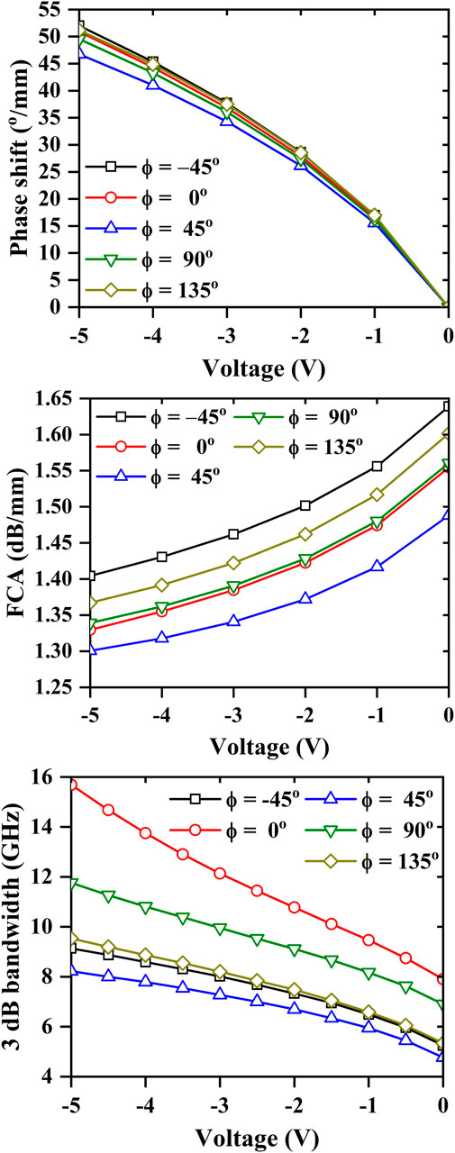
FIGURE 8. (A) Phase shift per unit length, (B) free-carrier absorption per unit length, and (C) 3-dB bandwidth for different wafer rotations at 7° tilt.
Wafer tilt and rotation during dopant implantation leads to a large variation in the bandwidth as seen from Figure 7C and Figure 8C. The image plot of the phase, absorption, and the 3 dB bandwidth for different wafer rotation and tilt angles at -5 V are shown in Figure 9A–C respectively. The lowest (highest) phase shift occurs for ϕ = -45° (ϕ = 90°) and θ = 1° (θ = 9°). The lowest (highest) FCA occurs for ϕ = 0° (ϕ = 45°) and θ = 9° (θ = 1°). The lowest (highest) 3 dB bandwidth occurs for ϕ = -45° (ϕ = 90°) and θ = 1° (θ = 9°). In all cases, the highest phase, lowest absorption, and largest 3 dB bandwidth occurs at 9° wafer tilt. The corresponding change between the highest and lowest values of the phase shift, FCA, and 3 dB bandwidth are ∼ 1.39×, ∼ 1.27×, and ∼ 3.58×, respectively.
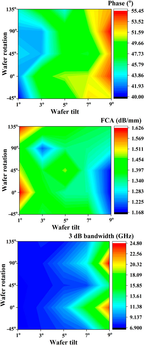
FIGURE 9. Image plot of (A) phase shift per unit length, (B) free-carrier absorption per unit length, and (C) 3-dB bandwidth at -5 V as a function of the wafer rotation and wafer tilt angles.
3.7 Pre-amorphization
Another effective way to stop ion channeling is to use a pre-amorphized wafer for implantation instead of tilting the wafer [42]. The substrate to be doped can be amorphized before dopant implantation by implanting silicon/germanium [43], carbon [44], or argon [41]. Thereafter, dopants are implanted into the amorphous host, followed by annealing. Comparison has been made between two phase shifters, one with a crystalline host (reference) and the other with an amorphous host. The phase shift and absorption loss per unit length is shown in Figures 10A, B respectively. The pre-amorphized sample has 1.31× higher phase shift and 1.28× lower FCA per unit length compared to the reference phase shifter. The PN phase shifter resistivity and capacitance of both samples are shown in Supplementary Figure S7 of the supplementary file. The modulation bandwidth is shown in Figure 10C for both samples, and it can be observed that the pre-amorphized sample has a 3-dB bandwidth of ∼37 GHz at -5 V, which is 5.17× higher than that of the reference phase shifter.
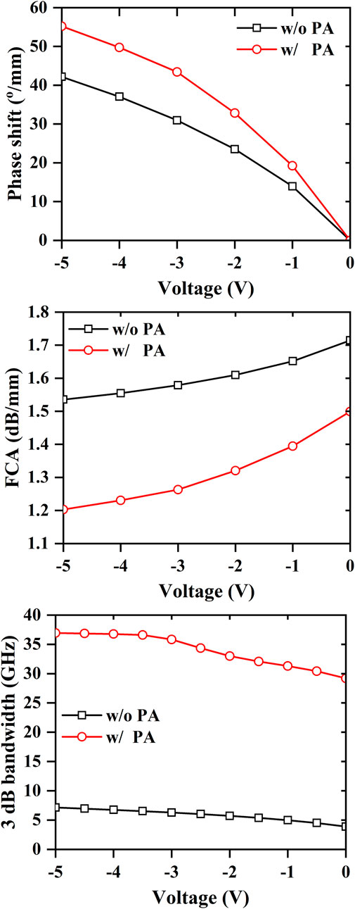
FIGURE 10. (A) Phase shift per unit length, (B) free-carrier absorption per unit length, and (C) 3-dB bandwidth for crystalline and pre-amorphized wafer (w/o PA: without pre-amorphization; w/PA: with pre-smorphization).
4 Discussion
From the previous section, it can be observed that each of the parameters have different effects on the phase shift, loss, and bandwidth. The phase shift is less dependent on the implantation energy, annealing, wafer temperature, and wafer rotation angle. The free-carrier absorption is dependent on all the process parameters taken in this study. The bandwidth is highly dependent on wafer tilt angle, rotation angle, and whether the host is crystalline or amorphous. The performance comparison of different process parameters is given in Table 1 at 5 V reverse bias voltage and phase shifter length for π phase shift. Increasing the implantation dose results in better modulation efficiency but at the expense of higher absorption. The bandwidth dependency is negligible for the simulated doses. A higher implantation energy results in low loss with no impact on the modulation efficiency. However, the FCA loss is dependent on the modal overlap with the free-carriers, and different implantation energy results in different depth profiles and, as such, will also depend on the waveguide dimension. A high-temperature, short-duration anneal results in better modulation efficiency but with higher loss and lower bandwidth. Implantation at room temperature results in low loss and high bandwidth compared to when the wafer is heated. The wafer tilt angle results in a marked difference in the phase shifter performance metrics. A large θ results in better modulation efficiency, low loss, and higher bandwidth. This is due to reduced channeling effect. For a 7° tilted wafer, rotating the wafer changes the performance metrics due to different degrees of channeling along different crystallographic planes. For the simulated phase shifter, ϕ = 0° results in low loss and high bandwidth. A ∼ 1.2× better modulation efficiency, ∼ 1.4× lower FCA, and ∼ 2.2× higher bandwidth is observed for a phase shifter with θ = 7°, ϕ = 0° compared to a phase shifter with θ = 0°, ϕ = 0° (reference). Implantation on a pre-amorphized substrate gives a ∼ 1.3× better modulation efficiency, ∼ 1.7× lower loss, and more than 5× higher bandwidth compared to implantation on a crystalline substrate (reference). The study shows that while the phase shifter performance metrics have different degrees of dependency on the process parameters, ion channeling is the main limiting factor. Tilting the wafer or amorphizing the substrate before implantation can greatly enhance the performance.
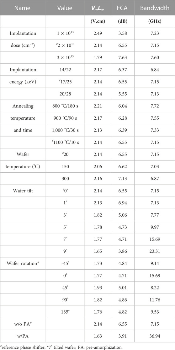
TABLE 1. Performance comparison of different process parameters at -5 V.
5 Conclusion
A process parameter study has been implemented in simulation using Silvaco® TCAD software to investigate the performance of a silicon optical PN phase shifter. The effect of the implantation dose, implantation energy, wafer temperature, annealing temperature and time, wafer tilt, wafer rotation, and pre-amorphization on the phase shift, absorption loss, and modulation bandwidth has been discussed. It has been observed that the phase shifter modulation bandwidth has a high degree of dependency on the wafer tilt, wafer rotation, and pre-amorphization compared to other process parameters. The ion channeling mechanism is found to be a limiting factor in the phase shifter performance and can be overcome by tilting or amorphizing the wafer. Compared to a reference phase shifter with 0° tilt and crystalline substrate, a 7° tilted crystalline wafer and a 0° tilted pre-amorphized wafer has 1.2× and 1.3× better modulation efficiency, 1.4× and 1.7× lower absorption, and 2.2× and 5.17× higher bandwidth at -5 V. Comparison of the 9° tilted sample and the pre-amorphized sample shows that both have the same modulation efficiency and free-carrier loss, but with 1.6× higher 3-dB bandwidth for the pre-amorphized sample at -5 V.
Data availability statement
The raw data supporting the conclusion of this article will be made available by the authors, without undue reservation.
Author contributions
DM and RS contributed to the conception, design, and analysis of the study. DM performed the simulations. All authors contributed to manuscript revision, read, and approved the submitted version.
Funding
This work is supported by the Science and Engineering Research Board (SERB), Ministry of Electronics and Information Technology (MeitY), and the Department of Science and Technology (DST-FIST), Government of India.
Conflict of interest
The authors declare that the research was conducted in the absence of any commercial or financial relationships that could be construed as a potential conflict of interest.
Publisher’s note
All claims expressed in this article are solely those of the authors and do not necessarily represent those of their affiliated organizations, or those of the publisher, the editors and the reviewers. Any product that may be evaluated in this article, or claim that may be made by its manufacturer, is not guaranteed or endorsed by the publisher.
Supplementary material
The Supplementary Material for this article can be found online at: https://www.frontiersin.org/articles/10.3389/fphy.2023.1123885/full#supplementary-material
References
1.LLP Mordor Intelligence. Photonic integrated circuit market - growth, trends, forecasts (2020-2025) ID: 5999324. Mordor Intelligence (2020). https://www.reportlinker.com/p05999324/Photonic-Integrated-Circuit-Market-Growth-Trends-Forecasts.html
2. Li N, Purnawirman P, Su Z, Magden ES, Callahan PT, Shtyrkova K, et al. High-power thulium lasers on a silicon photonics platform. Opt Lett (2017) 42:1181–4. doi:10.1364/ol.42.001181
3. Ellis S, Kuhlmann S, Kuehn K, Spinka H, Underwood D, Gupta R, et al. Photonic ring resonator filters for astronomical oh suppression. Opt express (2017) 25:15868–89. doi:10.1364/oe.25.015868
4. Sabella R. Silicon photonics for 5g and future networks. IEEE J Selected Top Quan Elect (2019) 26:1–11. doi:10.1109/jstqe.2019.2948501
5.Reports R. Global silicon photonics industry research report, competitive landscape, market size, regional status and prospect Maia-21532761 (2022).
6. Reed GT, Mashanovich G, Gardes FY, Thomson D. Silicon optical modulators. Nat Photon (2010) 4:518–26. doi:10.1038/nphoton.2010.179
7. Mishra D, Sonkar RK. Design and analysis of a graded-index strained si _{1−x} ge _x optical pn phase shifter. IEEE Photon J (2018) 10:1–14. doi:10.1109/jphot.2018.2880077
8. Zhalehpour S, Lin J, Guo M, Sepehrian H, Zhang Z, Rusch LA, et al. All-silicon iq modulator for 100 gbaud 32qam transmissions. In: Optical fiber communication conference. Washington D.C., United States: Optica Publishing Group (2019). Th4A–5.
9. Zhou J, Wang J, Zhu L, Zhang Q. Silicon photonics for 100gbaud. J Lightwave Tech (2020) 39:857–67. doi:10.1109/jlt.2020.3009952
10. Zhou J, Wang J, Zhu L, Zhang Q. High baud rate all-silicon photonics carrier depletion modulators. J Lightwave Tech (2019) 38:272–81. doi:10.1109/jlt.2019.2933384
11. Tong Y, Hu Z, Wu X, Liu S, Chang L, Netherton A, et al. An experimental demonstration of 160-gbit/s pam-4 using a silicon micro-ring modulator. IEEE Photon Tech Lett (2019) 32:125–8. doi:10.1109/lpt.2019.2960238
12. Gardes F, Brimont A, Sanchis P, Rasigade G, Marris-Morini D, O’Faolain L, et al. High-speed modulation of a compact silicon ring resonator based on a reverse-biased pn diode. Opt express (2009) 17:21986–91. doi:10.1364/oe.17.021986
13. Li K, Liu S, Thomson DJ, Zhang W, Yan X, Meng F, et al. Electronic–photonic convergence for silicon photonics transmitters beyond 100 gbps on–off keying. Optica (2020) 7:1514–6. doi:10.1364/optica.411122
14. Li M, Wang L, Li X, Xiao X, Yu S. Silicon intensity mach–zehnder modulator for single lane 100 gb/s applications. Photon Res (2018) 6:109–16. doi:10.1364/prj.6.000109
15. Samani A, El-Fiky E, Morsy-Osman M, Li R, Patel D, Hoang T, et al. Silicon photonic mach–zehnder modulator architectures for on chip pam-4 signal generation. J Lightwave Tech (2019) 37:2989–99. doi:10.1109/jlt.2019.2908655
16. Temporiti E, Ghilioni A, Minoia G, Orlandi P, Repossi M, Baldi D, et al. Insights into silicon photonics mach–zehnder-based optical transmitter architectures. IEEE J Solid-State Circuits (2016) 51:3178–91. doi:10.1109/jssc.2016.2593802
17. Samani A, Chagnon M, El-Fiky E, Patel D, Jacques M, Veerasubramanian V, et al. Silicon photonics modulator architectures for multi-level signal generation and transmission. In: Optical fiber communication conference. Washington D.C., United States: Optica Publishing Group (2017). Tu2H–4.
18. Sato H, Miura H, Qiu F, Spring AM, Kashino T, Kikuchi T, et al. Low driving voltage mach-zehnder interference modulator constructed from an electro-optic polymer on ultra-thin silicon with a broadband operation. Opt Express (2017) 25:768–75. doi:10.1364/oe.25.000768
19. Abel S, Eltes F, Ortmann JE, Messner A, Castera P, Wagner T, et al. Large pockels effect in micro-and nanostructured barium titanate integrated on silicon. Nat Mater (2019) 18:42–7. doi:10.1038/s41563-018-0208-0
20. Amin R, Maiti R, Gui Y, Suer C, Miscuglio M, Heidari E, et al. Sub-wavelength ghz-fast broadband ito mach–zehnder modulator on silicon photonics. Optica (2020) 7:333–5. doi:10.1364/optica.389437
21. Yu H, Bogaerts W, De Keersgieter A. Optimization of ion implantation condition for depletion-type silicon optical modulators. IEEE J Quan Elect (2010) 46:1763–8. doi:10.1109/jqe.2010.2067206
22. Yong Z, Sacher WD, Huang Y, Mikkelsen JC, Yang Y, Luo X, et al. U-shaped pn junctions for efficient silicon mach-zehnder and microring modulators in the o-band. Opt express (2017) 25:8425–39. doi:10.1364/oe.25.008425
23. Liu Y, Dunham S, Baehr-Jones T, Lim AE-J, Lo G-Q, Hochberg M. Ultra-responsive phase shifters for depletion mode silicon modulators. J lightwave Technol (2013) 31:3787–93. doi:10.1109/jlt.2013.2287697
24. Png CE, Sun MJ, Lim ST, Ang TY, Ogawa K. Numerical modeling and analysis for high-efficiency carrier-depletion silicon rib-waveguide phase shifters. IEEE J Selected Top Quan Elect (2016) 22:99–106. doi:10.1109/jstqe.2016.2564648
25. Hernández-Mangas J, Arias J, Bailón L, Jaraız M, Barbolla J. Improved binary collision approximation ion implant simulators. J Appl Phys (2002) 91:658–67. doi:10.1063/1.1424052
26. Tian S, Wang G, Morris M, Morris S, Obradovic B, Tasch A, et al. A computationally efficient ion implantation damage model and its application to multiple implant simulations. In: SISPAD’97. 1997 international conference on simulation of semiconductor processes and devices. Technical Digest IEEE (1997). 309–12.
27. Li D, Wang G, Chen Y, Lin L, Shrivastav G, Oak S, et al. A computationally efficient simulator for three-dimensional Monte Carlo simulation of ion implantation into complex structures. Nucl Instr Methods Phys Res Section B: Beam Interactions Mater Atoms (2001) 184:500–8. doi:10.1016/s0168-583x(01)00699-1
28. Tian S, Morris MF, Morris SJ, Obradovic B, Wang G, Tasch AF, et al. A detailed physical model for ion implant induced damage in silicon. Ieee Transactions Electron Devices (1998) 45:1226–38. doi:10.1109/16.678523
29. Hane M, Matsumoto H. A model for boron short time annealing after ion implantation. IEEE Transactions Electron Devices (1993) 40:1215–22. doi:10.1109/16.216424
30. Wu K, Zhao M, Yang T, da Costa JG, Liang Z, Shi X. Design and fabrication of low gain avalanche detectors (lgad): A tcad simulation study. J Instrumentation (2020) 15:C03008. doi:10.1088/1748-0221/15/03/c03008
31. Cao Z, Duan B, Song H, Xie F, Yang Y. Novel superjunction ldmos with a high-k dielectric trench by tcad simulation study. IEEE Trans Electron Devices (2019) 66:2327–32. doi:10.1109/ted.2019.2906911
32. Marcelot O, Goiffon V, Magnan P. Exploration of pinned photodiode radiation hardening solutions through tcad simulations. IEEE Trans Electron Devices (2019) 66:3411–6. doi:10.1109/ted.2019.2922755
33. Das P, Wu T-L, Tallur S. Design and analysis of high electron mobility transistor inspired: Iii-v electro-optic modulator topologies. Semiconductor Sci Tech (2020) 35:095028. doi:10.1088/1361-6641/ab9ea9
34. Bisognin G, De Salvador D, Napolitani E, Carnera A, Bruno E, Mirabella S, et al. Lattice strain induced by boron clusters in crystalline silicon. Semiconductor Sci Technol (2006) 21:L41–4. doi:10.1088/0268-1242/21/6/l01
35. Robinson MT, Torrens IM. Computer simulation of atomic-displacement cascades in solids in the binary-collision approximation. Phys Rev B (1974) 9:5008–24. doi:10.1103/physrevb.9.5008
36. Robinson MT. The binary collision approximation: Background and introduction. Radiat Effects Defects Sol (1994) 130:3–20. doi:10.1080/10420159408219767
37. Chroneos A, Bracht H, Grimes R, Uberuaga B. Phosphorous clustering in germanium-rich silicon germanium. Mater Sci Eng B (2008) 154:72–5. doi:10.1016/j.mseb.2008.08.005
38. Soref R, Bennett B. Electrooptical effects in silicon. IEEE J Quan Electron (1987) 23:123–9. doi:10.1109/jqe.1987.1073206
39. Zhou S, Wu H-t., Sadeghipour K, Scarcella C, Eason C, Rensing M, et al. Optimization of pam-4 transmitters based on lumped silicon photonic mzms for high-speed short-reach optical links. Opt express (2017) 25:4312–25. doi:10.1364/oe.25.004312
40. Narayan J, Holland O, Eby R, Wortman J, Ozguz V, Rozgonyi G. Rapid thermal annealing of arsenic and boron-implanted silicon. Appl Phys Lett (1983) 43:957–9. doi:10.1063/1.94200
41. Bresolin C, Zaccherini C, Anderle M, Canteri R. A comparison between zero and seven degrees of tilt implantation of as+, p+ and bf2+. Nucl Instr Methods Phys Res Section B: Beam Interactions Mater Atoms (1990) 51:122–4. doi:10.1016/0168-583x(90)90511-r
42. Al-Bayati A, Tandon S, Mayur A, Foad M, Wagner D, Murto R, et al. Exploring the limits of pre-amorphization implants on controlling channeling and diffusion of low energy b implants and ultra shallow junction formation. In: Proceeding of the 2000 International Conference on Ion Implantation Technology Proceedings. Ion Implantation Technology-2000 (Cat. No. 00EX432); September 2000; Alpbach, Austria. IEEE (2000). 54–61.
43. Ajmera A, Rozgonyi G, Fair R. Point defect/dopant diffusion considerations following preamorphization of silicon via si+ and ge+ implantation. Appl Phys Lett (1988) 52:813–5. doi:10.1063/1.99292
Keywords: phase shifter, photonics, process simulation, silicon, TCAD
Citation: Mishra D and Sonkar RK (2023) A TCAD study on the effect of process parameters on silicon optical phase shifter performance. Front. Phys. 11:1123885. doi: 10.3389/fphy.2023.1123885
Received: 15 December 2022; Accepted: 24 March 2023;
Published: 12 April 2023.
Edited by:
Yaping Dan, Shanghai Jiao Tong University, ChinaReviewed by:
SungWon Chung, Neuralink Corporation, United StatesKapil Debnath, Indian Institute of Technology Kharagpur, India
Copyright © 2023 Mishra and Sonkar. This is an open-access article distributed under the terms of the Creative Commons Attribution License (CC BY). The use, distribution or reproduction in other forums is permitted, provided the original author(s) and the copyright owner(s) are credited and that the original publication in this journal is cited, in accordance with accepted academic practice. No use, distribution or reproduction is permitted which does not comply with these terms.
*Correspondence: Ramesh Kumar Sonkar, c29ua2FyQGlpdGcuYWMuaW4=