 Si Li
Si Li Yuhan Gao
 Dongsheng Li
 Deren Yang
- State Key Lab of Silicon Materials, Department of Materials Science and Engineering, Zhejiang University, Hangzhou, China
Silicon pn-junction diodes with different doping concentrations were prepared by boron diffusion into Czochralski n-type silicon substrate. Their room-temperature near-infrared electroluminescence (EL) was measured. In the EL spectra of the heavily boron doped diode, a luminescence peak at ~1.6 μm (0.78 eV) was observed besides the band-to-band line (~1.1 eV) under the condition of high current injection, while in that of the lightly boron doped diode only the band-to-band line was observed. The intensity of peak at 0.78 eV increases exponentially with current injection with no observable saturation at room temperature. Furthermore, no dislocations were found in the cross-sectional transmission electron microscopy image, and no dislocation-related luminescence was observed in the low-temperature photoluminescence spectra. We deduce that the 0.78 eV emission originates from the irradiative recombination in the strain region of diodes caused by the diffusion of large number of the boron atoms into a silicon crystal lattice.
Introduction
With the development of integrated circuits (ICs), the disadvantage of traditional metal interconnection structure, such as interlayer interference, energy dissipation, and signal delay, has become a bottleneck restricting the development of ultra-large-scale integration circuits (USLIs). Optical interconnection, which uses photons to transform information, will be an ultimate solution for future progress in USLIs. Because silicon is an indirect-band-gap semiconductor and fundamentally unable to emit light efficiently, achieving efficient silicon-based light sources compatible with current IC manufacturing technology has become the key issue of silicon optoelectronics. Many routes to fabricate efficient silicon light emitters have been proposed: porous silicon (Canham, 1990; Qin et al., 1996; Bisi et al., 2000; Zhao et al., 2005a,b), Si nanoprecipitates in SiO2 (Pavesi et al., 2000; Wang et al., 2007), erbium-doped Si (Ennen et al., 1983; Zheng et al., 1994; Polman et al., 1995), Si/SiO2 superlattice structures (Lu et al., 1995), and silicon pn-junction diodes (Sveinbjörnsson, 1996; Martin et al., 2001; Ng et al., 2001; Sun et al., 2004; Lourenco et al., 2005). Among these ways, silicon pn-junction diodes have attracted much attention. The most standout advantage of this kind of light-emitter is that the fabrication process is totally compatible with USLI technology. Both ion-implantation (Sveinbjörnsson, 1996; Martin et al., 2001; Ng et al., 2001; Sun et al., 2004; Lourenco et al., 2005; Sobolev, 2010) and thermal diffusion (Kveder et al., 2004; Hoang et al., 2006, 2007) have been used to manufacture silicon pn diodes. The past few years has seen great advances in the development of silicon pn-junction diodes. Electroluminescence (EL) efficiency of 0.1–1% has been achieved (Martin et al., 2001; Ng et al., 2001). In addition to the band-to-band emission around 1.1 μm, other near-infrared emissions have been found in boron-implanted and boron-diffused silicon pn diodes (Sveinbjörnsson, 1996; Sun et al., 2004). Sveinbjörnsson (1996) reported strong ~1.6 μm (0.78 eV) EL emission related to dislocation-related center D1 at room temperature from dislocation-rich silicon diodes. Sun et al. (2004) reported two luminescence bands around 1.05 and 0.95 eV related to doping spikes in boron-implanted silicon pn diodes. These emissions show great application potential in silicon optoelectronics. But the mechanism is still in dispute.
In this paper, we fabricated silicon pn-junction diodes with different boron doping concentrations. Their room-temperature EL was measured and their cross-sectional transmission electron microscopy (TEM) images were studied. The result shows that the heavily boron doped silicon pn-junction diode without dislocation loops can emit strong 0.78 eV luminescence under the condition of high current injection besides the band-to-band emission. It is considered that the 0.78 eV emission originates from the irradiative recombination in the strain regions caused by the diffusion of large number of boron atoms into silicon crystal lattice.
Materials and Methods
Two kinds of boron diffusion sources were prepared by dissolving B2O3 into SiO2 latex with B3+ concentration of 0.203 mol/L (marked as A) and 0.569 mol/L (marked as B), respectively. Boron sources were spin onto the surface of (100) oriented n-type Czochralski-grown Si substrates (2 ~ 10 Ω cm, 500 μm in thickness) after the substrate wafer was cut into 15 mm × 15 mm slices and carefully cleaned by standard RCA process. Rapid thermal treating method was used to form shallow pn junction by boron diffusion at 1100°C for 5 min in the flowing high-purity N2 atmosphere. After a pn junction was formed, an indium tin oxide (ITO) electrode with a thickness of 100 nm was deposited on the p-layer side by magnetron sputtering, and an Al electrode with a thickness of 100 nm was evaporated on the n-layer side. Thus, a pn-junction diode was prepared.
The carrier concentration and the depth of pn junctions were studied by an SSM350 instrument of spreading resistance profile (SRP). The microstructure of pn junctions was measured by a transmission electron microscope (TEM, JEOL 2010). Photoluminescence (PL) and EL signals were recorded using an Edinburgh FLS920P Spectrometer with a nitrogen-cooled near-infrared photomultiplier tube. The low-temperature PL measurements were performed over the range of 20 ~ 300 K by using a helium flow cryostat.
Results and Discussion
Figure 1 is the SRP results of pn junctions made from the two boron sources (A and B). It is clear from the figure that shallow pn junctions were formed. It can be seen that Sample B made from the B boron source has the higher carrier concentration than Sample A made from the A boron source. The surface carrier concentration of Sample B reaches 4.6 × 1017 cm−3, while that of Sample A is 5 × 1016 cm−3. It is necessary to notify that the SPR measures the activated dopant density only, which does not take into account the possible dopant clustering at the surface, so there can be a large amount of boron doping, which is inactive. The depth of Sample B pn junction is about 250 nm, a little deeper than that of Sample A, which is about 200 nm.
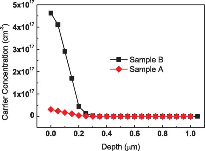
Figure 1. Spreading resistance profile spectra of pn junctions made from Sample A and Sample B fabricated with two boron sources.
Figure 2 shows the I–V curves of the two pn diodes. As shown in the figure, both the pn diodes perform good rectifying properties. The forward current increases quickly with the voltage while the reverse current stays low. Under the same forward bias, the current of Sample B is greater than that of Sample A. This is because Sample B has the higher carrier concentration and less resistance. In addition, the turn-on voltage of Sample B is about 0.7 V, bigger than that of Sample A, which is about 0.6 V. The reason is that the pn-junction barrier of Sample B with higher doping concentration is larger, so that the forward voltage needed to overcome the barrier is larger.
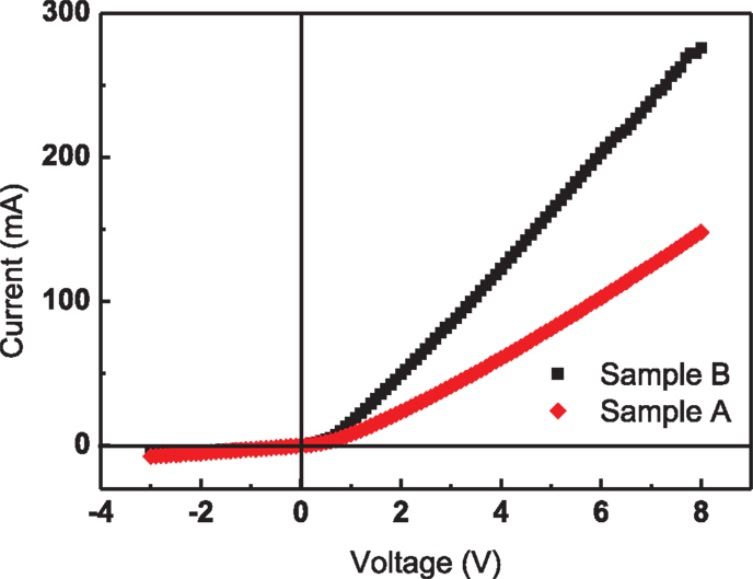
Figure 2. I–V curves of the two pn diodes at room temperature.
The room-temperature EL spectra of Sample B and Sample A are different, as shown in Figure 3. In the room-temperature EL spectra of Sample A, only band-to-band emission is observed as the current increases. In contrast, Sample B emits 0.78 eV EL besides the band-to-band emission under the condition of high current injection (>705 mA) and its intensity increases greatly with the current. The band-to-band emission of both pn diodes demonstrates a small red shift with the increasing current; this is related to the device heating in response to the current injection.
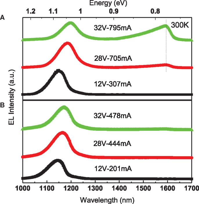
Figure 3. Room-temperature EL spectra at different electrical currents of two pn diodes: (A) for sample B and (B) for sample A.
Sveinbjörnsson (1996) and Xiang et al. (2012a,b) have reported strong emission of 0.78 eV EL at room temperature from silicon pn diodes containing dislocations. They have also found dislocation-related bands in the low-temperature PL spectra. They tended to regard the peak at 0.78 eV in PL spectrum at room temperature as a red-shifted luminescence band D1. However, for Sample B, no other luminescence band is found in the low-temperature PL spectrum (the pump power intensity is 0.22 W/cm2) except the band-to-band emission and no dislocations are observed in the cross-sectional TEM image as shown in Figure 4. It can be seen from Figure 4B that Sample B is free from dislocations. Our work suggests that the 0.78 eV EL at room temperature has no direct connection with dislocations or dislocation-related luminescence bands. In fact, lots of lattice damage regions can be seen near the surface of Sample B in the TEM image. As mentioned before, although the measured dopant concentration by SPR is relatively low, a significant amount of inactive boron doping may exist, so we think that the observed lattice distortion is caused by large number of boron atoms diffusing into silicon lattice. Under the condition of high current injection, these regions can trap carriers and form effective irradiative recombination centers, which are related to the 0.78 eV luminescence.
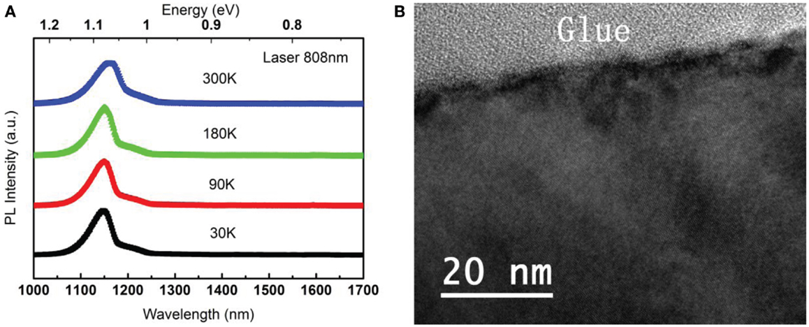
Figure 4. (A) Photoluminescence spectra registered at different temperatures under laser excitation of 808 nm (500 mW) and (B) cross-sectional TEM image of sample B.
Figure 5 shows the dependence of peak intensity of 0.78 eV on the input power. When the input power is low, there is no 0.78 eV EL emission. When the input power reaches ~15 W, Sample B starts to emit 0.78 eV luminescence and its intensity increases almost exponentially with the input power with no observable saturation. This means that if the turn-on power of the o.78 eV emission could be sufficiently decreased, a highly efficient light source would be achieved.
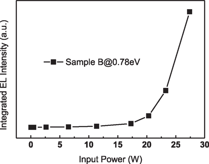
Figure 5. The dependence of peak intensity of EL band at 0.78 eV on the input power of pn-junction diodes.
Conclusion
In this paper, two silicon pn diodes with different boron doping concentrations were fabricated by boron diffusion. We studied their room-temperature near-infrared EL. The results show that in the EL spectra of the heavily boron doped diode, a luminescence peak at ~1.6 μm (0.78 eV) was observed besides the band-to-band line (~1.1 eV) under the condition of high current injection, while in that of the lightly boron doped diode, only the band-to-band line was observed. In addition, no dislocations were found in the cross-sectional TEM image and no dislocation-related luminescence was observed in the low-temperature PL spectra. The 0.78 eV emission is proved to have no direct connection with dislocations or dislocation-related luminescence bands. In fact, lots of lattice damage regions can be seen near the surface of the highly doped diode in the TEM image. We deduce that the 0.78 eV emission may originate from the irradiative recombination in these regions. What is more, the intensity of 0.78 eV emission increases exponentially with the input power without observable saturation, which may be used as an efficient light source in future.
Conflict of Interest Statement
The authors declare that the research was conducted in the absence of any commercial or financial relationships that could be construed as a potential conflict of interest.
Acknowledgments
This work is supported by the National Basic Research Program of China (973 Program) (No. 2013CB632102).
References
Bisi, O., Ossicini, S., and Pavesi, L. (2000). Surf. Sci. Rep. 38, 1–126. doi: 10.1016/S0167-5729(99)00012-6
Canham, L. T. (1990). Silicon quantum wire array fabrication by electrochemical and chemical dissolution of wafers. Appl. Phys. Lett. 57, 1046–1048. doi:10.1063/1.103561
Ennen, H., Schneider, J., Pomerenke, G., and Axmann, A. (1983). 1.54-μm Luminescence of erbium implanted III–V? semiconductors and silicon. Appl. Phys. Lett. 43, 943–945. doi:10.1063/1.94190
Hoang, T., Holleman, J., LeMinh, P., Schmitz, J., Mchedlidze, T., Arguirov, T., et al. (2007). Influence of dislocation loops on the near-infrared light emission from silicon diodes. IEEE Trans. Electron Devices 54, 1860–1866. doi:10.1109/TED.2007.901072
Hoang, T., LeMinh, P., Holleman, J., and Schmitz, J. (2006). Strong efficiency improvement of SOI-LEDs through carrier confinement. IEEE Electron Device Lett. 27, 383–385. doi:10.1109/LED.2007.895415
Kveder, V., Badylevich, M., Steinman, E., Lzotov, A., Seibt, M., and Schroter, W. (2004). Room-temperature silicon light-emitting diodes based on dislocation luminescence. Appl. Phys. Lett. 84, 2106–2108. doi:10.1063/1.1689402
Lourenco, M. A., Milosavljevic, M., Galata, S., Siddiqui, M. S. A., Shao, G., Gwilliam, R. M., et al. (2005). Silicon-based light-emitting devices. Vacuum 78, 551–556. doi:10.1016/j.vacuum.2005.01.085
Lu, Z. H., Lockwood, D. J., and Baribeau, J. M. (1995). Quantum confinement and light emission in SiO2/Si superlattices. Nature 378, 258–260. doi:10.1038/378258a0
Pubmed Abstract | Pubmed Full Text | CrossRef Full Text | Google Scholar
Martin, A. G., Zhao, J., Wang, A., Peter, J. R., and Michal, G. (2001). Efficient silicon light-emitting diodes. Nature 412, 805–808. doi:10.1038/35090539
Pubmed Abstract | Pubmed Full Text | CrossRef Full Text | Google Scholar
Ng, W. L., Lourenco, M. A., Gwilliam, R. M., Ledain, S., Shao, G., and Hoomwood, K. P. (2001). An efficient room-temperature silicon-based light-emitting diode. Nature 410, 192–194. doi:10.1038/35069092
Pubmed Abstract | Pubmed Full Text | CrossRef Full Text | Google Scholar
Pavesi, L., Dal, N. L., Mazzoleni, C., Franzo, G., and Priolo, F. (2000). Optical gain in silicon nanocrystals. Nature 408, 440–444. doi:10.1038/35044012
Polman, A., Van, D., Hoven, G. N., Custer, J. S., Shin, J. H., and Sema, R. (1995). Erbium in crystal silicon: optical activation, excitation, and concentration limits. J. Appl. Phys. 77, 1256–1262. doi:10.1063/1.358927
Qin, G. G., Song, H. Z., Zhang, B. R., Lin, J., Duan, J. Q., and Yao, G. Q. (1996). Experimental evidence for luminescence from silicon oxide layers in oxidized porous silicon. Phys. Rev. B 54, 2548–2555. doi:10.1103/PhysRevB.54.2548
Sobolev, N. A. (2010). Defect engineering in implantation technology of silicon light-emitting structures with dislocation-related luminescence. Semiconductors 44, 1–23. doi:10.1134/S106378261001001X
Sun, J. M., Dekorsy, T., Skorupa, W., Schmdt, B., Mucklich, A., and Helm, M. (2004). Below-band-gap electroluminescence related to doping spikes in boron-implanted silicon pn diodes. Phys. Rev. B 70, 1–11. doi:10.1103/PhysRevB.70.155316
Sveinbjörnsson, E. Ö, and Weber, J. (1996). Room temperature electroluminescence from dislocation-rich silicon. Appl. Phys. Lett. 69, 2686–2688. doi:10.1063/1.117678
Wang, M., Li, D., Yuan, Z., Yang, D., and Que, D. (2007). Photoluminescence of Si-rich silicon nitride: defect-related states and silicon nanoclusters. Appl. Phys. Lett. 90, 1–3. doi:10.1063/1.2717014
Xiang, L., Li, D., Jin, L., and Yang, D. (2012a). Dislocation-related electroluminescence of silicon after electron irradiation. Solid State Commun. 152, 1956–1959. doi:10.1016/j.ssc.2012.08.011
Xiang, L., Li, D., Jin, L., Pivac, B., and Yang, D. (2012b). The origin of 0.78eV line of the dislocation related luminescence in silicon. J. Appl. Phys. 112, 1–4. doi:10.1063/1.4754825
Zhao, Y., Yang, D., Li, D., and Jiang, M. (2005a). Annealing and amorphous silicon passivation of porous silicon with the blue light emission. Appl. Surf. Sci. 252, 1065–1069. doi:10.1016/j.apsusc.2005.01.176
Zhao, Y., Yang, D., Li, D., and Jiang, M. (2005b). Photoluminescence of oxidized porous silicon under UV-light illumination. Mater. Sci. Eng. B 116, 95–98. doi:10.1016/j.mseb.2004.08.014
Pubmed Abstract | Pubmed Full Text | CrossRef Full Text | Google Scholar
Keywords: boron diffusion, silicon pn-junction diode, near-infrared electroluminescence
Citation: Li S, Gao Y, Fan R, Li D and Yang D (2015) Room-temperature near-infrared electroluminescence from boron-diffused silicon pn-junction diodes. Front. Mater. 2:8. doi: 10.3389/fmats.2015.00008
Received: 17 August 2014; Accepted: 20 January 2015;
Published online: 23 February 2015.
Edited by:
Dan-Xia Xu, National Research Council Canada, CanadaReviewed by:
Jifeng Liu, Dartmouth College, USATatiana S. Perova, The University of Dublin, Ireland
Copyright: © 2015 Li, Gao, Fan, Li and Yang. This is an open-access article distributed under the terms of the Creative Commons Attribution License (CC BY). The use, distribution or reproduction in other forums is permitted, provided the original author(s) or licensor are credited and that the original publication in this journal is cited, in accordance with accepted academic practice. No use, distribution or reproduction is permitted which does not comply with these terms.
*Correspondence: Deren Yang, State Key Lab of Silicon Materials, Department of Materials Science and Engineering, Zhejiang University, Zheda Road 38, Hangzhou 310027, China e-mail:bXNleWFuZ0B6anUuZWR1LmNu