 Tatsurou Hiraki
 Hiroshi Fukuda3
 Koji Yamada
- 1NTT Device Technology Laboratories, NTT Corporation, Kanagawa, Japan
- 2NTT Nanophotonics Center, NTT Corporation, Kanagawa, Japan
- 3NTT Device Innovation Center, NTT Corporation, Kanagawa, Japan
We demonstrated a small sensitivity to temperature variations of delay-line Mach–Zehnder interferometer (DL MZI) on a Si photonics platform. The key technique is to balance a thermo-optic effect in the two arms by using waveguide made of different materials. With silicon and silicon nitride waveguides, the fabricated DL MZI with a free-spectrum range of ~40 GHz showed a wavelength shift of -2.8 pm/K with temperature variations, which is 24 times smaller than that of the conventional Si-waveguide DL MZI. We also demonstrated the decoding of the 40-Gbit/s differential phase-shift keying signals to on-off keying signals with various temperatures. The tolerable temperature variation for the acceptable power penalty was significantly improved due to the small wavelength shifts.
Introduction
Silicon (Si) photonics is one of the most promising technologies for overcoming the limitations on integration in commercially available silica-based planar-lightwave circuits. This is because it provides ultra-compact waveguides and makes the monolithic integration of active and passive devices possible (Lockwood and Pavesi, 2010; Vivien and Pavesi, 2013). Many compact devices, such as arrayed-waveguide gratings, Mach–Zehnder interferometers (MZIs), and ring resonators, have been reported using Si (Fukazawa et al., 2004; Xia et al., 2007) and silicon nitride (SiN) waveguides (Gondarenko et al., 2009; Chen et al., 2011). One of the issues with these devices is performance degradation with temperature variations due to the thermo-optic (TO) coefficient’s of Si (~1.86 × 10⁻⁴/K) and SiN (4 ~ 5 × 10⁻⁵/K) being higher than that of the silica (~1.0 × 10⁻⁵/K). To overcome this issue, athermal designs of Si-waveguide delay line (DL) MZIs have used different effective-index changes with temperature (dneff/dT) in the two arms to balance the TO effects in them (Uenuma and Motooka, 2009; Guha et al., 2010; Hai and Liboiron-Ladouceur, 2011). In the previous studies, dneff/dT was controlled by means of the different optical confinement in the Si cores of narrow and wide Si waveguides. However, the dneff/dT of the narrow waveguides significantly depended on the core width; therefore, inevitable fabrication errors made it difficult to minimize the TO effect. To prevent the problem, the dneff/dT should be controlled by changing the TO coefficients of the materials, without using a narrow waveguide. In our previous work, we reported control of the refractive indices and TO coefficients of complementary metal-oxide semiconductor (CMOS) compatible materials by changing the atomic composition of SiOx, SiOxNy, and SiN (Tsuchizawa et al., 2011; Nishi et al., 2012; Hiraki et al., 2013). Using these materials, in this work, we minimized the temperature sensitivity of the DL MZI. In the following sections, we show the details of the design and fabrication of the DL MZI and present experimental results. In addition, as a feasibility demonstration, we show the thermal stability of the decoding of differential phase-shift eying (DPSK) signals to on-off keying (OOK) signals at 40 Gbit/s.
Design and Fabrication
Figure 1 shows a schematic of the DL MZI. The temperature sensitivity could be minimized by balancing the TO effect between the two arms, while keeping the differential delay between them. The interference condition is expressed as following equation (Guha et al., 2010)
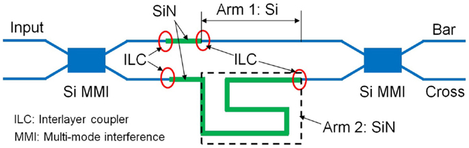
Figure 1. Schematic of Si–SiN-waveguide DL MZI.
Here, m is an integer for constructive interference or a half-integer destructive interference, neff, 1 and neff, 2 are the effective indices, and L1 and L2 are the physical lengths of arm 1 and 2. Then, the temperature sensitivity of the interference spectrum could be obtained by differentiating above equation with respect to temperature, as expressed by following
Athermal condition is given by the numerator of this equation to be 0. Since we have two design parameters L1 and L2, we can make dλ/dT to be 0 while keeping the differential delay. The key technique is to control dneff/dT by changing the core materials of the two arms. In this work, we used Si and SiN waveguides in the CMOS compatible materials. In the design, the refractive index and the TO coefficient of the SiN core are 2.0 and 4.0 × 10⁻⁵/K, respectively. The core thicknesses of the waveguides were fixed at 220 and 400 nm, respectively. Figure 2 shows the calculated results of relationships between dneff/dT and the core widths of the Si and SiN waveguides. For little change of the dneff/dT with width variations, we used a 440-nm-wide Si waveguide as arm 1, and an 800-nm-wide SiN-waveguide as arm 2, respectively. We designed the DL MZI with a free spectral range (FSR) of 40 GHz. The FSR is given by the inverse of the differential delay, or 1-bit delay time Δt = (ng, 2 L2 - ng, 1 L1)/c, where ng, 1 and ng, 2 are group indices of the arm 1 and 2, and c is the speed of light in vacuum. Under this differential delay condition, the dλ/dT can be 0 by choosing the L1 and L2 as 0.95 mm and 5.77 mm, respectively. It is notable that if we could use the state-of-the-art fabrication process with width variations of 3 nm (Shimura et al., 2014), the dλ/dT could be less than 0.1 pm/K, which is over 10 times smaller than that using a 280-nm-wide (narrow) Si-waveguide as arm 2 (Hai and Liboiron-Ladouceur, 2011) with the same width variations.
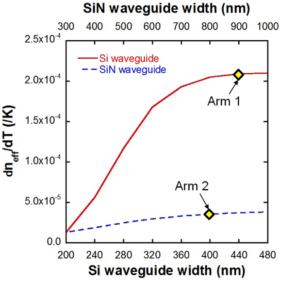
Figure 2. Relationships between dneff/dT and core width of Si and SiN waveguides.
As other features to construct the DL MZI structure, we used the inverse taper of the Si waveguide for the fiber-chip interface, and 2 × 2 Si-waveguide multimode interference (MMI) couplers. The taper-tip width and the taper length of the fiber-chip interface were 200 nm and 300 μm, respectively. Since the Si and SiN waveguides were formed in different layers, the interlayer coupler (ILC) between them was designed using adiabatically tapers (Huang et al., 2014). We introduced the ILCs into both arms to cancel out their phase delays. In addition, as reference samples, we designed a conventional Si-waveguide DL MZI and a SiN-waveguide DL MZI without any compensation for thermal sensitivity (dneff, 1/dT = dneff,2/dT). In the conventional DL MZIs, both arms comprised of the same structures, which were the 440-nm-wide Si waveguide and the 800-nm-wide SiN waveguide.
The DL MZI was fabricated on an 8-inch silicon-on-insulator wafer, whose buried-oxide thickness was 3 μm. The Si waveguides were first patterned; then, a clad film was deposited. After that, the clad film was flattened, and SiN-waveguide cores were formed. The interlayer clad thickness between the Si and SiN waveguides was controlled to be 100 nm. Finally, an overclad film was deposited. A microscope image of the fabricated Si–SiN-waveguide DL MZI is shown in Figure 3. The total size of the fabricated DL MZI is ~0.56 mm2/ch, which is comparable to that of the conventional SiN-waveguide DL MZI. It is still larger than that of the Si-waveguide DL MZI; however, it is several-hundred times smaller than one made of the commercially-used silica.
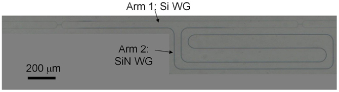
Figure 3. Microscope image of fabricated Si–SiN-waveguide DL MZI.
Results and Discussions
We measured transmission spectra of the fabricated DL MZI. We used a tunable laser diode (TLD) as a light source and swept the wavelength of the input light, and measured output light power from the bar port. The input and output fibers were lensed fibers with mode-field diameters of ~3.5 μm, and the polarization of the input light was adjusted to the transverse electric (TE) mode. The chip was set on a temperature-controlled stage by using a heat-dissipation tape. We measured the transmission spectra of the DL MZIs, while varying the chip-stage temperature range from 298–302 K so that the wavelength shift should not exceed the FSR. Figures 4A–C show the transmission spectra of the Si–SiN-waveguide DL MZI, the conventional SiN-waveguide DL MZI, and the conventional Si-waveguide DL MZI at 298 and 300 K. The output powers were normalized by the fiber-to-fiber transmission spectra. It is clear that the Si–SiN-waveguide DL MZI highly suppresses the wavelength shift with temperature variations. The measured FSRs and the dλ/dT are listed in Table 1. The TO effects of the fabricated SiN- and Si waveguides are almost consistent with their designs. The dλ/dT of the Si-SiN DL MZI is over six times smaller than that of the conventional SiN waveguide, and 24 times smaller than that of the conventional Si-waveguide DL MZI. Although the dλ/dT of the Si–SiN DL MZI is larger than the expected value (<0.1 pm/K) because of the large fabrication error over 3 nm, the measured result is still better than those for DLI MZIs with narrow Si waveguides (Uenuma and Motooka, 2009; Guha et al., 2010). The FSR of the Si–SiN DL MZI is 40.5 GHz, which is only about 1% different from the target value. The insertion loss of the Si–SiN-waveguide DL MZI is ~13 dB, which includes the fiber-chip coupling loss of ~2 dB/facet and the interlayer coupling loss of ~0.5 dB/couple. The extinction ratio is ~17 dB, which is mainly determined by an imbalance of propagation loss between two arms of the MZI and an unintentional imbalance of the MMI branch. The propagation loss of SiN and Si waveguides are ~12 dB/cm and ~4 dB/cm, respectively. The unintentional imbalance of the MMI branch is ~1.3 dB. Although the imbalance between two arms is large, the imbalance of the MMI branch improves the extinction ratio. The insertion loss and extinction ratio would be further improved because a well-controlled fabrication environment would reduce the SiN-waveguide loss (Huang et al., 2014). We must mention that the device was designed for only TE mode light. For polarization diversity circuits (Fukuda et al., 2008), a polarization rotator using parallel cores has already been demonstrated using the same Si and SiN layers as in this work (Fukuda and Wada, 2014).
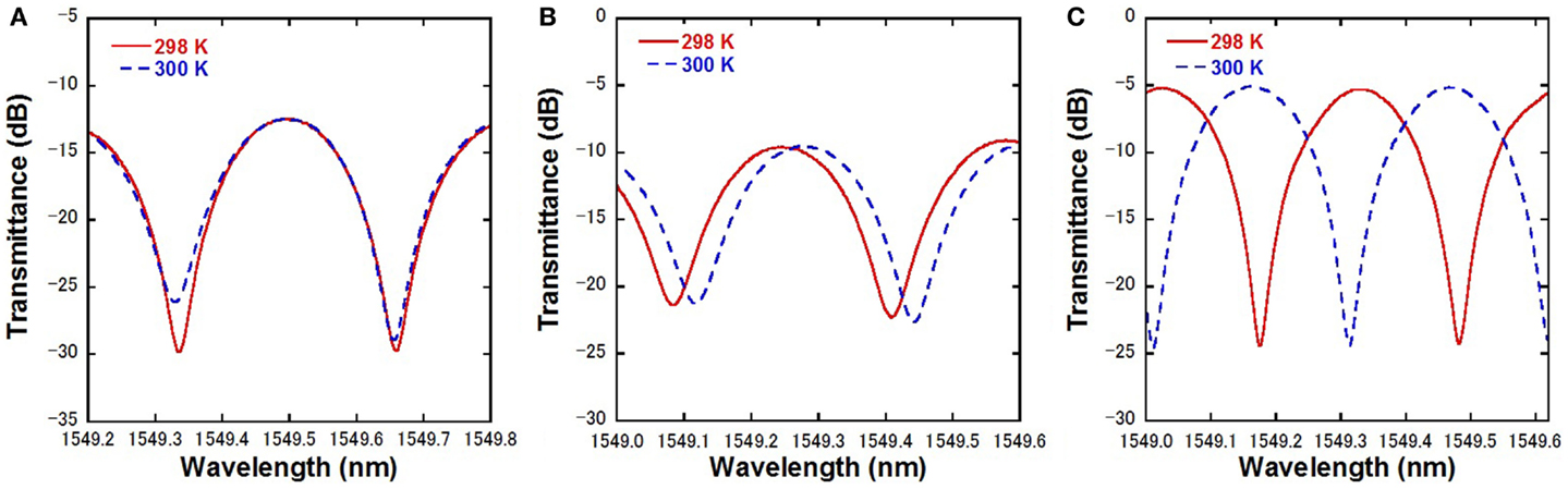
Figure 4. Transmission spectra of (A) Si–SiN-waveguide DL MZI, (B) SiN-waveguide DL MZI, and (C) Si-waveguide DL MZI.
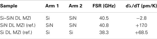
Table 1. Measured FSRs and dλ/dT.
As a feasibility demonstration, we applied the Si–SiN-waveguide DL MZI to decode 40-Gbit/s DPSK signals. Figure 5 shows the experimental setup. We input the DPSK signals with a non-return-to-zero (NRZ) 40-Gbit/s pseudo-random bit sequence (PRBS) of length 231 - 1. The eye diagram of the input signals is shown in the inset of Figure 5. The polarization state of the input light was adjusted to the TE mode. The output light was coupled by the lensed fiber and then switched to the optical spectrum analyzer or the photodiode. The electrical signals from the photodiode were amplified then fed into the sampling oscilloscope. Figures 6A,B show the constructive- and destructive-interference spectra of the bar port at frequency of 193.611 and 193.592 THz, respectively. They were measured at 298 K. The decoded 40-Gbit/s signals were observed as 40-GHz-span dips in the destructive-interference spectra. Their eye diagrams are shown in the insets of Figures 6A,B, respectively. Here, the vertical axis is 20 mV/div and the horizontal axis is 10 ps/div. The two output signals carried logically inverted data streams in the DPSK format. The constructive interference carried duobinary, whereas the destructive-interference carries alternate-mark inversion (Gnauck and Winzer, 2005). Using the destructive interference, we demonstrated a thermal tolerance to decode the DPSK format to the OOK format (Winzer and Leuthold, 2001; Lazzeri et al., 2010). Figures 7A,B show the eye diagrams of the destructive-interference signals at 299 and 302 K, respectively. The eye diagrams clearly open at 302 K, corresponding to a temperature variation of 4 K from the initial temperature (298 K). From the measured dλ/dT of -2.8 pm/K, the estimated frequency shift by the temperature variation of +4 K is -1.4 GHz, which could cause only about 1-dB penalty for a 40-Gbit/s system (Hoon and Winzer, 2003). By using the state-of-the-art fabrication process, as discussed in the above section, the tolerable temperature variations could be over 90 K. As references, the eye diagrams of the conventional Si-waveguide DL MZI at 298 and 299 K are shown in Figures 8A,B, respectively. Here, the vertical axis is 69.7 mV/div and the horizontal axis is 10.0 ps/div. The eye diagram was completely closed with a temperature variation of only +1 K. These results clearly show that the Si–SiN-waveguide DL MZI actually improves the thermal-insensitivity of the Si-photonic DL MZI and that it has a potential to be used in the telecommunications devices. A well-controlled fabrication environment would reduce the insertion loss of the DL MZI and also improves the signal-to-noise ratio.
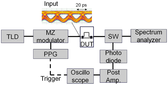
Figure 5. Experimental setup for decoding of 40-Gbit/s DPSK signals.
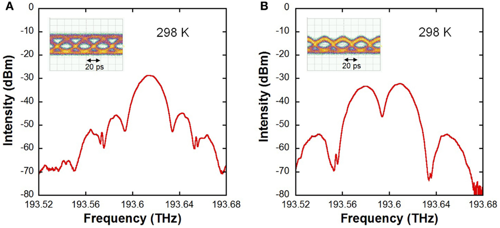
Figure 6. Decoded-signal spectra and eye diagrams (insets) of (A) constructive- and (B) destructive interference at 298 K.
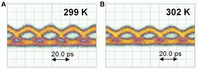
Figure 7. Eye diagrams of Si–SiN-waveguide DL MZI at (A) 299 and (B) 302 K.
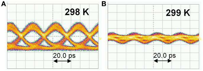
Figure 8. Eye diagrams of Si-waveguide DL MZI at (A) 298 and (B) 299 K.
Conclusion
We demonstrated a small sensitivity to temperature variations of DL MZI on a Si-photonics platform. The key technique is to balance the TO effect in two arms by using waveguides made of different materials, which are Si and SiN. The Si–SiN-waveguide DL MZI with an FSR of 40 GHz showed dλ/dT of -2.8 pm/K, which is about 24 times smaller than that of the conventional Si-waveguide DL MZI. The technology has the potential to reduce temperature sensitivities of various Si-photonic devices, such as wavelength filters, phase demodulators, and ring resonators.
Conflict of Interest Statement
The authors declare that the research was conducted in the absence of any commercial or financial relationships that could be construed as a potential conflict of interest.
References
Chen, L., Doerr, C. R., Dong, P., and Chen, Y. K. (2011). Monolithic silicon chip with 10 modulator channels at 25 Gbps and 100-GHz spacing. Opt. Express 19, B946–B951. doi: 10.1364/OE.19.00B946
Pubmed Abstract | Pubmed Full Text | CrossRef Full Text | Google Scholar
Fukazawa, T., Ohno, F., and Baba, T. (2004). Very compact arrayed-waveguide-grating demultiplexer using Si photonic wire waveguides. Jpn. J. Appl. Phys. 43, L673–L675. doi:10.1143/JJAP.43.L673
Fukuda, H., and Wada, K. (2014). Parallel-core-type polarization rotator for silicon wire waveguide platform. Photonics Res. 2, A14–A18. doi:10.1364/PRJ.2.000A14
Fukuda, H., Yamada, K., Tsuchizawa, T., Watanabe, T., Shinojima, H., and Itabashi, S. (2008). Silicon photonic circuit with polarization diversity. Opt. Express 16, 4872–4880. doi:10.1364/OE.16.004872
Pubmed Abstract | Pubmed Full Text | CrossRef Full Text | Google Scholar
Gnauck, A. H., and Winzer, P. J. (2005). Optical phase-shift-keyed transmission. J. Lightw. Technol. 23, 115–130. doi:10.1109/JLT.2004.840357
Gondarenko, A., Levy, J. S., and Lipson, M. (2009). High confinement micron-scale silicon nitride high Q ring resonator. Opt. Express 17, 11366–11370. doi:10.1364/OE.17.011366
Pubmed Abstract | Pubmed Full Text | CrossRef Full Text | Google Scholar
Guha, B., Gonarenko, A., and Lipson, M. (2010). Minimizing temperature sensitivity of silicon Mach-Zehnder interferometers. Opt. Express 18, 1879–1887. doi:10.1364/OE.18.001879
Pubmed Abstract | Pubmed Full Text | CrossRef Full Text | Google Scholar
Hai, M. S., and Liboiron-Ladouceur, O. (2011). “Temperature compensated 50 Gb/s DPSK demodulator,” in Conference on Lasers and Electro-Optics (Baltimore: OSA), JTuI76.
Hiraki, T., Nishi, H., Tsuchizawa, T., Kou, R., Fukuda, H., Takeda, K., et al. (2013). Si-Ge-Silica monolithic integration platform and its application to a 22-Gb/s x 16-ch WDM receiver. Photonics J. 5, 4500407. doi:10.1109/JPHOT.2013.2269676
Hoon, K., and Winzer, P. J. (2003). Robustness to laser frequency offset in direct-detection DPSK and DQPSK systems. J. Lightw. Technol. 21, 1887–1891. doi:10.1109/JLT.2003.816816
Huang, Y., Song, J., Luo, X., Liow, T. Y., and Lo, G. Q. (2014). CMOS compatible monolithic multi-layer Si3N4-on-SOI platform for low-loss high performance silicon photonics dense integration. Opt. Express 22, 21859–21865. doi:10.1364/OE.22.021859
Pubmed Abstract | Pubmed Full Text | CrossRef Full Text | Google Scholar
Lazzeri, E., Nguyen, A. T., Serafino, G., Kataoka, N., Wada, N., Bogoni, A., et al. (2010). “All-optical NRZ-DPSK to RZ-OOK format conversion using optical delay line interferometer and semiconductor optical amplifier,” in Photonics in Switching Conference (Monterey), JTuB45.
Nishi, H., Tsuchizawa, T., Kou, R., Shinojima, H., Yamada, T., Kimura, H., et al. (2012). Monolithic integration of a silica AWG and Ge photodiodes on Si photonic platform for one-chip WDM receiver. Opt. Express 20, 9312–9321. doi:10.1364/OE.20.009312
Pubmed Abstract | Pubmed Full Text | CrossRef Full Text | Google Scholar
Shimura, D., Horikawa, T., Okayama, H., Jeong, S.-H., Tokushima, M., Sasaki, H., et al. (2014). “High precision Si waveguide devices designed for 1.31μm and 1.55μm wavelengths on 300mm-SOI,” in Conference on Group IV Photonics. Vancouver: IEEE.
Tsuchizawa, T., Yamada, K., Watanabe, T., Sungbong, P., Nishi, H., Kou, R., et al. (2011). Monolithic integration of silicon-, germanium-, and silica-based optical devices for telecommunications applications. IEEE J. Sel. Top. Quant. Electron. 17, 516–525. doi:10.1109/JSTQE.2010.2089430
Uenuma, M., and Motooka, T. (2009). Temperature-independent silicon waveguide optical filter. Opt. Lett. 34, 599–601. doi:10.1364/OL.34.000599
Vivien, L., and Pavesi, L. (eds). (2013). Handbook of Silicon Photonics. New York: Taylor and Francis.
Winzer, P. J., and Leuthold, J. (2001). Return-to-zero modulator using a single NRZ drive signal and an optical delay interferometer. IEEE Photon. Technol. Lett. 13, 1298–1300. doi:10.1109/68.969887
Xia, F., Rooks, M., Sekaric, L., and Vlasov, Y. (2007). Ultra-compact high order ring resonator filters using submicron silicon photonic wires for on-chip optical interconnects. Opt. Express 15, 11934–11941. doi:10.1364/OE.15.011934
Pubmed Abstract | Pubmed Full Text | CrossRef Full Text | Google Scholar
Keywords: silicon photonics, thermo-optic effect, Mach-Zehnder interferometer, waveguide, silicon nitride
Citation: Hiraki T, Fukuda H, Yamada K and Yamamoto T (2015) Small sensitivity to temperature variations of Si-photonic Mach–Zehnder interferometer using Si and SiN waveguides. Front. Mater. 2:26. doi: 10.3389/fmats.2015.00026
Received: 16 January 2015; Accepted: 16 March 2015;
Published online: 30 March 2015.
Edited by:
Toshihiko Baba, Yokohama National University, JapanReviewed by:
Junichi Fujikata, Photonics Electronics Technology Research Association, JapanYosuke Terada, Yokohama National University, Japan
Copyright: © 2015 Hiraki, Fukuda, Yamada and Yamamoto. This is an open-access article distributed under the terms of the Creative Commons Attribution License (CC BY). The use, distribution or reproduction in other forums is permitted, provided the original author(s) or licensor are credited and that the original publication in this journal is cited, in accordance with accepted academic practice. No use, distribution or reproduction is permitted which does not comply with these terms.
*Correspondence: Tatsurou Hiraki, Device Technology Laboratories, NTT corporation, 3-1, Morinosato Wakamiya, Atsugi-shi, Kanagawa 243-0198, Japan e-mail:aGlyYWtpLnRhdHN1cm91QGxhYi5udHQuY28uanA=