 Jutta Schwarzkopf
 Dorothee Braun1
 Martin Schmidbauer
- 1Leibniz Institute for Crystal Growth, Berlin, Germany
- 2Paul Drude Institute for Solid-State Electronics, Berlin, Germany
The application of lattice strain through epitaxial growth of oxide films on lattice mismatched perovskite-like substrates strongly influences the structural properties of ferroelectric domains and their corresponding piezoelectric behavior. The formation of different ferroelectric phases can be understood by a strain-phase diagram, which is calculated within the framework of the Landau–Ginzburg–Devonshire theory. In this paper, we illustrate the opportunity of ferroelectric domain engineering in the KxNa1−xNbO3 lead-free material system. In particular, the following examples are discussed in detail: (i) Different substrates (NdGaO3, SrTiO3, DyScO3, TbScO3, and GdScO3) are used to systematically tune the incorporated epitaxial strain from compressive to tensile. This can be exploited to adjust the NaNbO3 thin film surface orientation and, concomitantly, the vector of electrical polarization, which rotates from mainly vertical to exclusive in-plane orientation. (ii) In ferroelectric NaNbO3, thin films grown on rare-earth scandate substrates, highly regular stripe domain patterns are observed. By using different film thicknesses, these can be tailored with regard to domain periodicity and vertical polarization component. (iii) A featured potassium concentration of x = 0.9 of KxNa1−xNbO3 thin films grown on (110) NdScO3 substrates favors the coexistence of two equivalent, monoclinic, but differently oriented ferroelectric phases. A complicated herringbone domain pattern is experimentally observed which consists of alternating MC and a1a2 domains. The coexistence of different types of ferroelectric domains leads to polarization discontinuities at the domain walls, potentially enabling high piezoelectric responses. In each of these examples, the experimental results are in excellent agreement with predictions based on the linear elasticity theory.
Introduction
Perovskite-like oxide materials with ferro- and piezoelectric properties are used for a wide range of memory, actuator, sensor, or RF devices (Haertling, 1999; Setter et al., 2006). So far, the commonly used materials are based on lead-containing compounds due to their excellent physical properties. However, owing to their ecological and healthy issues, they need to be replaced by environmentally friendlier materials, which—however—often exhibit diminished characteristics. In order to obtain equivalent or even better ferro- and piezoelectric properties in lead-free materials, structural modifications have been shown to be a practical approach (Schlom et al., 2007; Damodaran et al., 2016). Due to the inherent coupling between structure and functionality, this provides the opportunity for a targeted engineering of their properties. It has been shown that “giant” piezoelectric responses can be provoked when the electrical polarization vector has the ability to continuously rotate within the unit cell (Noheda, 2002; Davis et al., 2007). This situation can be, for example, achieved in materials exhibiting a monoclinic phase symmetry (Vanderbilt and Cohen, 2001). An alternative pathway to mimic this rotational effect is the coexistence of different types of ferroelectric domains in the material with an abrupt change of the polarization vector at the domain walls (Catalan et al., 2011; Lee and Noh, 2012).
An adequate tool for structural modifications is the epitaxial growth of strained thin films on substrates with tailored lattice mismatch. However, for a directive tuning of the functional properties of thin films, a detailed understanding of the correlation between lattice strain and ferroelectric phase formation is required. Such information can be obtained from strain-phase diagrams derived e.g., from the analysis of the Gibbs free energy in the framework of the Landau–Ginzburg–Devonshire (LGD) theory (Pertsev et al., 1998). Importantly, due to clamping of the film on a bulky substrate higher orders of the Taylor expansion have to be taken into account to image the anisotropic biaxial stress (Pertsev et al., 1998; Zembilgotov et al., 2008; Liang et al., 2009). To further exploit the effect of polarization discontinuities in multi-domain arrangements, selected film-substrate combinations have to be chosen which enable the coexistence of differently oriented ferroelectric phases. The required stress conditions, which determine strain state and surface orientation of the epitaxial films, can be reliably predicted by linear elasticity theory (Hammerschmidt et al., 2007). The combination of both—strain-phase diagrams and elasticity theory—provides extensive and versatile possibilities for strain engineering of ferroelectrics.
With regard to previously mentioned aspects, lead-free KxNa1−xNbO3 is an ideal candidate. On the one hand, it exhibits promising ferro-/piezoelectric properties even as bulk material. On the other hand, when epitaxially deposited on a substrate, its orthorhombic crystal symmetry yields the possibility to incorporate anisotropic lattice strain into the thin film. Moreover, the epitaxial strain can be systematically varied by tuning the film composition x or by the use of different substrates (see Figure 1). At the Leibniz Institute for Crystal Growth (IKZ), a unique variety of high-quality orthorhombic substrates (e.g., rare-earth scandates ReScO3 with Re = Dy, Tb, Gd, Sm, Nd, Pr) with a wide range of lattice parameters are grown (Uecker et al., 2013). Some of them are used for the purpose of this study. As a result, epitaxial strain can be tailored from compressive to tensile in small, precise steps.
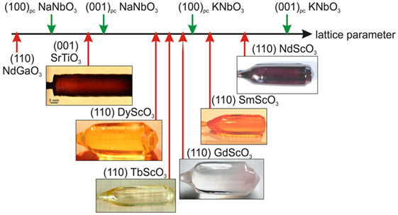
Figure 1. Schematic presentation of the pseudocubic (pc) lattice parameters of NaNbO3 and KNbO3 (end members of the solid-solution KxNa1−xNbO3) as well as the average in-plane lattice parameters of different perovskite-like substrate surfaces. The rare-earth scandates ReScO3 (Re = Dy, Tb, Gd, Sm, Nd) are all grown at the Leibniz Institute for Crystal Growth (Uecker et al., 2006, 2008, 2013; Coh et al., 2010; Guguschev et al., 2015). A part of the figure is reproduced from Guguschev et al. (2015) with permission from the Royal Society of Chemistry.
In this paper, we will experimentally verify (i) the emergence of ferroelectric monoclinic phases and (ii) the tuning of thin film orientation (or even coexistence of two surface orientations) by adequate incorporation of lattice strain. For that purpose, NaNbO3 thin films on different lattice mismatched substrates and K0.9Na0.1NbO3 thin films on NdScO3 substrates have been grown epitaxially.
Experimental
The KxNa1−xNbO3 thin films were grown by liquid-delivery spin metal-organic chemical vapor deposition (MOCVD). This method proceeds close to thermodynamic equilibrium at increased oxygen partial pressure compared to physical methods such as pulsed laser deposition or sputtering. Consequently, it provides highly perfect films with smooth surfaces and interfaces as well as a nearly stoichiometric composition. All films were grown at a substrate temperature of 973 K, a substrate rotation of 750 rpm and an oxygen to argon ratio in the gas phase of 0.63 at a gas pressure of 2.6⋅103 Pa. K(thd), Na(thd) [(thd) = 2,2,6,6-tetramethyl-3,5-heptanedione], and Nb(EtO)5 [(EtO)5 = pentaethoxide] were used as metal–organic source materials dissolved in dry toluene. For more details, see Schwarzkopf et al. (2012).
Unless otherwise noted, all films were grown directly on the bare substrate without a bottom electrode in order to avoid premature lattice relaxation. Before introducing the perovskite substrates (with a 0.1° off-orientation) into the reactor chamber, they were annealed in pure oxygen gas flow in order to generate a regular step-and-terrace surface structure and a well-defined surface termination. The SrTiO3 substrates were also etched in a buffered HF solution (Koster et al., 1998) prior to the introduction into the baking furnace. For each substrate, an optimum annealing temperature has been determined: 1,050°C for NdGaO3, 1,100°C for SrTiO3, 1,050°C for DyScO3, 1,150°C for TbScO3, and 1,050°C for GdScO3. While the DyScO3, TbScO3, and GdScO3 substrates were grown at Leibniz Institute for Crystal Growth, the NdGaO3 and SrTiO3 are commercial substrates (CrysTec).
An atomic force microscope (AFM) was used to analyze the surface morphology. The Asylum Research MFP-3D stand-alone AFM is equipped with a piezoresponse force microscopy (PFM) mode realized as dual AC resonance tracking version. This mode enables a simultaneous measurement of the surface morphology of the film along with its piezoelectric response. If the electric polarization has a component in vertical direction, the cantilever exhibits a deflection. In case of a lateral component, the cantilever experiences a torsion. Finally, two types of signal can be recorded, denoted as vertical and lateral PFM, respectively (Gruverman et al., 1996; Soergel, 2011). As a result of the applied AC voltage, the ferroelectric domains react in-phase or out-of-phase to the initial bias yielding the possibility to differentiate between different electrical polarization directions in adjacent domains. Due to the measurement at the resonance frequency of the cantilever, the signal-to-noise ratio can be significantly increased. Thus, the ferroelectric domain structure of thin films can be measured with a spatial resolution of a few nanometers.
Structural characterization of the films was performed by various X-ray diffraction techniques. Among these is out-of-plane high-resolution X-ray diffraction (HR-XRD) that was carried at a commercial instrument (Bruker D8 Discover) using a monochromatic (λ = 1.54056 Å) and well collimated (angular resolution better that 0.1 mrad) X-ray beam. A linear position sensitive detector was used to perform fast two-dimensional mapping of reciprocal space. Samples with film thicknesses down to a few nanometers can be investigated. In-plane structural information was obtained by grazing-incidence X-ray diffraction (GIXD) which was carried out at intense synchrotron radiation sources (ESRF, DESY and BESSY). For these measurements, the glancing angle of incidence is chosen slightly above the critical angle of total external reflection leading to a strong suppression of the scattering signal from the substrate and, thus, to maximum sensitivity to the thin film. Similar to HR-XRD, two-dimensional in-plane reciprocal space maps were recorded by utilizing a position sensitive detector (Schmidbauer et al., 2008).
In order to distinguish between strain (e.g., vertical and lateral lattice parameters, monoclinic distortion angle) and morphology (e.g., domain size and periodicity, domain wall orientation, film thicknesses) related features in reciprocal space, it is necessary to investigate a variety of different in-plane and out-of-plane Bragg reflections.
Strain-Phase Diagram of KNbO3 and Film Orientation
Calculation of the misfit strain – misfit strain-phase diagram (in the following referred to as strain-phase diagram) for room temperature was performed in the framework of the LGD theory. Within the scope of this theory, a Taylor expansion of the Gibbs free energy G(T,P) is used with the ferroelectric polarization vector P as order parameter at a temperature T. Due to the fact that in epitaxial growth the film is clamped to a bulky substrate, parts of the energy functions do no longer describe a free standing material. In consequence, for calculating the strain-phase diagram, a Legendre transformation of the Gibbs free energy G has to be performed to change the parameter set from G(T,P) to (T, εxx, εyy, P) (Pertsev et al., 1998; Wang and Zhang, 2005; Zembilgotov et al., 2005), where εxx and εyy are the in-plane normal strain components along the two in-plane directions x and y, respectively. The modified potential , which is eight-order polynomial, has to be minimized with respect to every polarization component (P1, P2, P3) to determine the equilibrium thermodynamic state of the thin film. Since the focus of this work was not on the simulation part, we omitted to give the expression for the potential , rather an interested reader is referred to the paper from Zembilgotov et al. (2008). In practice, for determination of the strain-phase diagram, for every strain configuration {εxx, εyy} the minimum of has to be calculated in dependence of P1, P2, and P3. For that purpose, the material parameters elastic compliances (classify the resistance a material opposes its mechanical deformation), electrostrictive constants (describe the deformation of a dielectric material in dependence of the applied electric field) and dielectric stiffnesses (display the maximum electric field that a material can withstand without breaking down) are required. In thin films under anisotropic strain conditions, different equilibrium states can occur: (i) p phase (P1 = P2 = P3 = 0), (ii) a1 phase (P1 ≠ 0 and P2 = P3 = 0), (iii) a2 phase (P2 ≠ 0 and P1 = P3 = 0), (iv) c phase (P3 ≠ 0 and P1 = P2 = 0), (v) a1a2 phase (P1 ≠ 0, P2 ≠ 0 and P3 = 0), (vi) a1c or Mc phase (P1 ≠ 0 and P3 ≠ 0, P2 = 0), (vii) a2c or Mc phase (P2 ≠ 0 and P3 ≠ 0, P1 = 0), and (viii) r or MA/MB phase (P1 ≠ 0, P2 ≠ 0 and P3 ≠ 0).
It has to be noted that the calculations have been performed for a mono-domain case, the formation of poly-domains is not considered here. Furthermore, the elastic constants are reported for KNbO3 only (Bai and Ma, 2010), while they are not available for NaNbO3 or KxNa1−xNbO3. Thus, strictly speaking, only the phase diagram of KNbO3 can be calculated. But since we assume similar coefficients for NaNbO3 or the KxNa1−xNbO3 solid-solutions, we also refer for the phase predictions for these materials to the strain-phase diagram of KNbO3 calculated for room temperature.
For determination of the crystallographic film–substrate relationship, it is oftentimes advantageous to change from the orthorhombic to the pseudocubic lattice parameter set via the transformation rules given by Vailionis et al. (2011). In Figure 2A, the relationship between the orthorhombic (red) and pseudocubic (green) unit cells is schematically depicted. From this illustration, it can be seen that the pseudocubic unit cell exhibits monoclinic symmetry with two non-perpendicular axes (apc and cpc) and a monoclinic distortion angle β, which describes the deviation of the angle between bpc and cpc from 90° (β = 90° − αpc). The orthorhombic and pseudocubic lattice parameters of KxNa1−xNbO3 with x = 0 and x = 0.9 are given in Table 1, labeled by the indices “o” and “pc,” respectively. In contrast to the pseudocubic notation of the film planes and directions, for the orthorhombic gallate and scandate substrates, we always use the orthorhombic Miller indices. Here, surface directions and Bragg reflections are labeled by the substrate subscript (e.g., TSO for TbScO3).
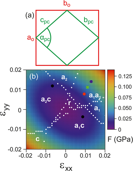
Figure 2. (A) Schematic presentation of the orthorhombic (red) and pseudocubic (green) unit cells of KxNa1−xNbO3. The angle αpc is connected to the monoclinic distortion angle β by αpc = 90°−β. (B) Calculated strain-phase diagram for KNbO3 using Landau–Ginzburg–Devonshire theory. The black circles indicate the strain conditions for (001)pc and (100)pc oriented K0.9Na0.1NbO3 on (110) NdScO3, while the red, green, and blue circles illustrate the situation for (100)pc oriented NaNbO3 on (110) DyScO3, TbScO3, and GdScO3, respectively. The white circles mark the stability transition points.

Table 1. Orthorhombic (index “o”) and pseudocubic (index “pc”) lattice parameters together with the monoclinic distortion angle β for NaNbO3 and K0.9Na0.1NbO3.
In Figure 2B, the strain-phase diagram is presented for KNbO3. Strain configurations {εxx, εyy}, where stability conditions change, are plotted as “stability transition points” marked as white circles. It is obvious that different monoclinic domains (see a1c/a2c or MC, r or MA and a1a2 in Figure 2B) can be realized in a wide range of strain conditions by an adequate application of lattice stress in the KNbO3 thin films. This circumstance confirms the choice of KNbO3 (or more generally KxNa1−xNbO3) as promising film material. However, our result exhibits differences to existing calculations for this material (Bai and Ma, 2010) with regard to the position of the phase transition lines. Indeed, this could be crucial for film-substrate combinations nearby these boundaries (see, for example, in chapter 6 below).
The strain-phase diagram does not give any information on the most favorable KxNa1−xNbO3 film orientation. The (001)pc and (100)pc surface orientations are not equivalent, they exhibit a monoclinic distortion in different directions, experience different strain conditions, and thus lead to different directions of the electrical polarization vectors. The unit cell orientation critically depends on the (anisotropic) lattice mismatch to the underlying substrate. In order to figure out the energetically most favorable surface orientation, linear elasticity theory can be used [for more detail, see Schwarzkopf et al. (2014)]. These calculations provide the elastic strain energy density that is associated for a specific crystallographic orientation. These calculations take into account the elastic anisotropy of the KxNa1−xNbO3 material system (Bai and Ma, 2010). In this context, it has to be regarded that both KxNa1−xNbO3 and most substrates exhibit orthorhombic crystal symmetry providing different lattice strain for (001)pc oriented films after a 90° in-plane rotation of the unit cell.
In the following, we will first consider the influence of the used substrate on the surface orientation of NaNbO3 thin films. Subsequently, we will highlight two different cases in the calculated strain-phase diagram:
i. Monoclinic a1a2 stripe domains with pure in-plane polarization by introducing tensile lattice in NaNbO3 films.
ii. Coexistence of monoclinic a1a2 and MC domains with pure in-plane and inclined polarization vector, respectively, by adjusting the composition in KxNa1−xNbO3 thin films on NdScO3 substrates.
Surface Orientation of NaNbO3 Thin Films on Different Substrates
According to the lattice parameters of film and substrate material given in Tables 1 and 2, respectively, the in-plane lattice strains εxx and εyy are determined both for (100)pc and (001)pc oriented NaNbO3 thin films on (110) NdGaO3, DyScO3, TbScO3, and GdScO3 orthorhombic substrates as well as on (001) SrTiO3 cubic substrate. Subsequently, the elastic strain energy density F(ε) is calculated for each substrate and for each orientation of the film unit cell. This is illustrated in Figure 3A. The bright and dark blue squares represent the result for the two (001)pc variants, while the red circles describe the elastic strain energy density for the (100)pc orientation. The expected surface orientation for NaNbO3 thin films on a (110) NdGaO3 substrate is (001)pc, resulting from a significantly lower energy density compared to the (100)pc variant. By contrast, for all rare-earth scandates, F(ε) is always significantly lower for (100)pc than for (001)pc orientation (Figure 3A) presumably resulting in a (100)pc orientation. NaNbO3 on SrTiO3 presents an almost lattice matched system. Consequently, the differences in F(ε) are too small as to show a clear preference. As a result, elastic strain considerations predict a transition from (001)pc surface orientation at compressive in-plane strain induced by NdGaO3 to (100)pc orientation for tensile film growth on rare-earth scandates.
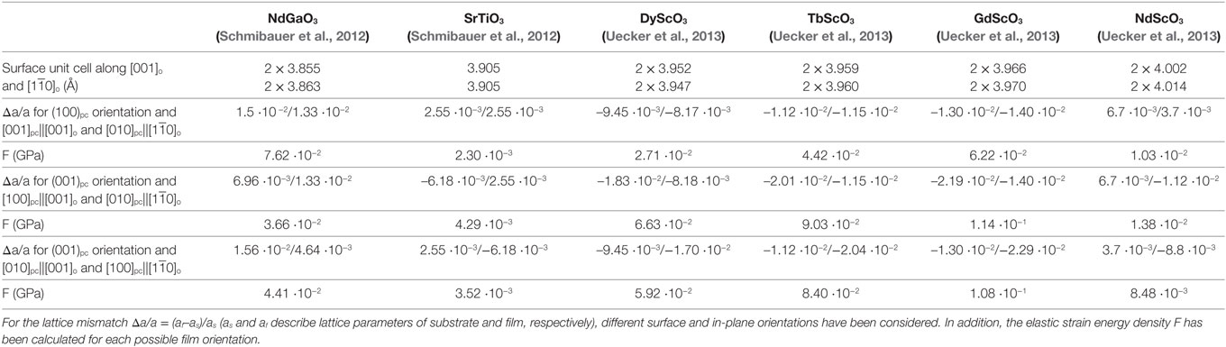
Table 2. Lattice parameters of different substrates as well as the corresponding lattice mismatches in [001]o and [1-10]o directions of the orthorhombic (index “o”) substrates ([100]c and [010]c in case of the cubic SrTiO3) for NaNbO3 on NdGaO3, SrTiO3, DyScO3, TbScO3, GdScO3, and for K0. 9Na0. 1NbO3 on NdScO3 (right column).
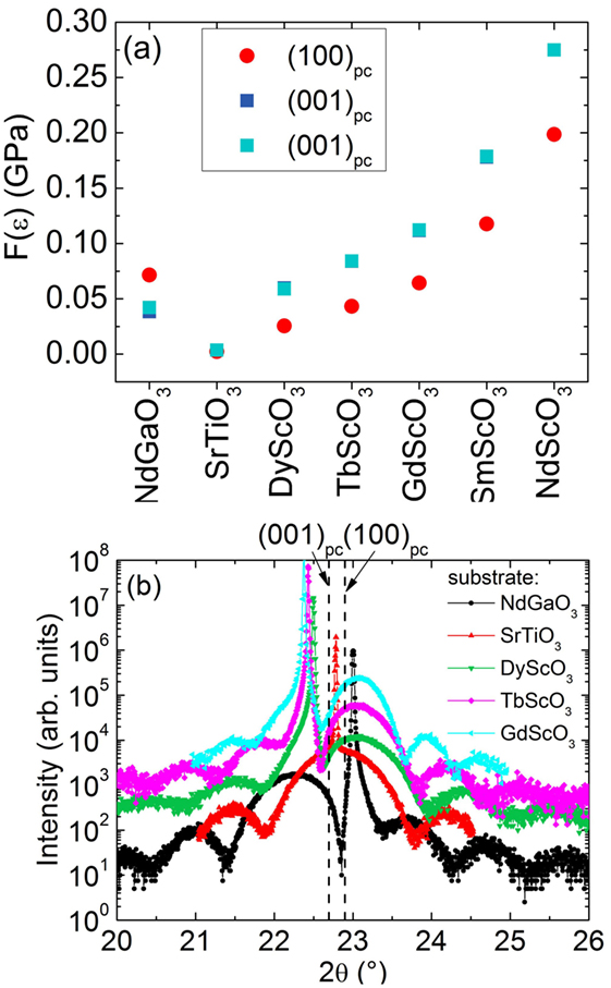
Figure 3. (A) Calculated elastic strain energy density F(ε) for (100)pc and (001)pc surface orientation of NaNbO3 films grown on different substrates. (B) High-resolution X-ray diffraction θ/2θ scans of 10 nm thick NaNbO3 films on the different substrates. The dashed lines indicate the positions for unstrained NaNbO3.
The elastic strain energy calculations were experimentally verified by growing NaNbO3 films on the different substrates. The film thickness was restricted to 10–15 nm ensuring fully strained films (Schwarzkopf et al., 2012). AFM images prove a rather smooth surface morphology (not shown here) with an average root mean square (rms) surface roughness of less than 0.3 nm. Strain state and orientation of the unit cells is evaluated for each case from HR-XRD measurements (Figure 3B). For that purpose, nominal peak positions for unstrained NaNbO3 are additionally given as dashed lines in the HR-XRD scans. The angular position of the Bragg reflection of the strained NaNbO3 thin film on NdGaO3 is shifted relative to the (001)pc bulk position to lower values which indicates compressive lattice strain in a (001)pc oriented NaNbO3 film. By contrast, the angular positions of film Bragg reflections on ReScO3 (Re = Dy, Tb, Gd) substrates occur at larger values than the corresponding bulk (100)pc position. This points to (100)pc oriented NaNbO3 thin films grown under tensile lattice strain. Film orientation and strain state of NaNbO3 on SrTiO3 cannot be unambiguously determined due to the overlapping of film and substrate peak and the large angular width of the film peak, which is caused by the small film thickness.
Summarizing, we conclude that the NaNbO3 film orientation switches from (001)pc on NdGaO3 to (100)pc on ReScO3 (Re = Dy, Tb, Gd) in agreement with the elastic strain energy calculations (Figure 2A). Concomitantly, the vector of electrical polarization rotates from mainly vertical to exclusive in-plane orientation (Schwarzkopf et al., 2014). Hence, an exact prediction of the unit cell orientation can be made as first step for domain engineering.
Monoclinic Stripe Domains in Tensely Strained NaNbO3 Thin Films on ReScO3 Substrates (Re = Dy, Tb, Gd)
In the strain-phase map in Figure 2B, the biaxial strain values for NaNbO3 on the different rare-earth scandates are introduced as circles (color index, see figure caption). Obviously, the occurrence of monoclinic a1a2 domains is expected for NaNbO3 thin films that are grown fully strained on these substrates.
Lateral PFM images for 10 nm thick films on the ReScO3 substrates show a pronounced stripe domain pattern (exemplarily shown for TbScO3 (TSO) substrate in Figure 4A) (Duk et al., 2013; Schmidbauer et al., 2014; Schwarzkopf et al., 2014). The in-plane phase signal is periodically modulated on the scale of a few tens of nanometers and the domain walls contain the [001]TSO direction. No vertical polarization component has been detected. Based on the observed contrast in the LPFM images, two arrangements of the polarization vectors with uncharged domain walls are possible and are presented in Figure 4C: a 180° (left) and a 90° (right) configuration.
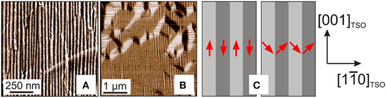
Figure 4. Lateral piezoresponse force microscopy image of a 10 nm NaNbO3 film (A) and a 60 nm NaNbO3 film (B) on a (110) TbScO3 (TSO) substrate. (C) Possible in-plane arrangements of polarization vectors in the stripe domains with 180° (left) and 90° (right) domain.
In order to verify the orientation of the polarization vectors and to analyze the phase symmetry, X-ray diffraction has been performed. Here again, we exemplarily present and discuss the system NaNbO3/TbScO3. Out-of-plane reciprocal space maps have been taken around the (444)TSO and (260)TSO substrate reciprocal lattice points. For both Bragg reflections (exemplarily shown for (444)TSO in Figure 5A) neither a vertical splitting of the film peak nor satellite peaks close to the film peak could be observed.
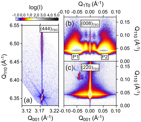
Figure 5. (A) X-ray reciprocal space maps around the (444)TSO substrate Bragg reflection. Grazing incidence in-plane X-ray diffraction map in the vicinity of (008)TSO (B) and (220)TSO (C) substrate Bragg reflections.
By contrast, GIXD performed nearby the (008)TSO substrate Bragg reflection (Figure 5B) reveals a pronounced horizontal peak splitting of the film contribution (marked as P1 and P2 in Figure 5B) along Q10, i.e., perpendicular to the domain walls. By contrast, for the intensity distribution in the vicinity of the (20)TSO substrate Bragg reflection, where the scattering vector is collinear to the domain stripes, no peak splitting is found (Figure 5C). The observed behavior can be explained by an alternate in-plane shearing (±β) of the film unit cells along [001]TSO in adjacent domains leading to a monoclinic symmetry of the unit cells (Figure 6A). On the other hand, the monoclinic lattice of two adjacent domains is coherent at the domain walls. The corresponding in-plane orientation of the electrical polarization vectors within the domains is also delineated in Figure 6A by red arrows and rotates by 90° for neighboring domains. This corresponds to the situation schematically presented in Figure 4C (right). The X-ray and PFM data prove that the thin film consists of a1a2 domains, which is in agreement with the predictions from the strain-phase diagram in Figure 2B. As long as the films are fully strained, these results can be transferred to NaNbO3 deposited on DyScO3 and GdScO3.
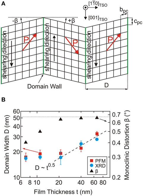
Figure 6. (A) Schematic presentation of the monoclinic shearing of the pseudocubic unit cells and resulting polarization vector (red arrows). Adjacent domains are sheared in opposite directions (black arrows). The monoclinic angles ± β are exaggeratedly illustrated. (B) Domain width D (red squares and blue circles deviated from PFM and X-ray measurements, respectively, left axis) and monoclinic angle β (black triangles, right axis) versus film thickness for NaNbO3 films grown on TbScO3 substrates.
It is very instructive to investigate the effect of film thickness on the domain pattern. Thereby film properties can systematically change: (i) while for very thin films the unit cell is adapted to the rectangular unit cell of the substrate (β = 0), the film lattice can elastically relax by increasing the monoclinic shearing angle up to the bulk value (Figure 6B, black triangles, right axis). This value is reached at a film thickness of about 20 nm. (ii) Just at this thickness, a 90° rotated domain variant evolves, i.e., the one-dimensional domain pattern is transformed into a two-dimensional domain pattern (Figure 4B). This transformation correlates with the onset of plastic strain relaxation through formation of misfit dislocations and a corresponding increase of the vertical lattice parameter (Schwarzkopf et al., 2012; Duk et al., 2013). Consequently, NaNbO3 films relax in a 2-step process, first elastically and subsequently plastically. (iii) The transformation from a one- to a two-dimensional domain pattern is accompanied by a characteristic increase of the lateral domain size. The domain width scales with the square root of film thickness (Figure 6B, red squares and blue circles, left axis) referred as Kittel law for ferromagnetics and ferroelectrics, which was extended to ferroelastics by Roitburd (1976). (iv) In addition, a vertical polarization component may evolve (Schmidbauer et al., 2014), indicating the occurrence of MB domains. The last point can also be inferred from Figure 2B: when in-plane lattice strains εxx and εyy are reduced, the stability region changes from a1a2 to r (which corresponds under tensile strain to MB domains exhibiting both lateral and vertical polarization components).
Summarizing, for (100)pc oriented NaNbO3 thin films grown under tensile lattice strain on ReScO3 substrates a periodic arrangement of a1a2 domains with pure in-plane polarization is observed as long as the films are fully strained. Reduction of the in-plane lattice strain by increasing the film thickness leads to MB domains with an additional out-of-plane component of the electrical polarization vector. These results are in full agreement with expectations from the strain-phase diagram.
K0.9Na0.1NbO3 Thin Films on NdScO3 Substrates
As mentioned before, the piezoelectric response can be largely enhanced in ferroelectrics when they (i) exhibit monoclinic symmetry or (ii) consist of domain walls with an abrupt change of the polarization alignment. Therefore, a combined approach containing both aspects would be most advantageous in order to maximize the mechanical deformation under an applied bias voltage. This goal can be achieved by combining strain-phase calculations and elasticity considerations. In a first step, we have evaluated the strain-phase diagram in order to determine strain conditions that provide the formation of monoclinic phases. From Figure 2B, it is obvious that indeed MC and MA phases, which both exhibit monoclinic symmetry, are energetically favorable for KNbO3 for low tensile and/or compressive lattice strain and a1a2 for larger tensile lattice strain.
To fulfill the second demand (coexistence of differently oriented domains or phases to provide polarization discontinuities at domain walls), the elastic strain energy densities F(ε) of (001)pc and (100)pc oriented phases of KxNa1−xNbO3 on a perovskite substrates have to be regarded [note, that for (001)pc orientation a 90° in-plane rotation (blue curve) is not equivalent to a 0° variant (cyan curve)]. We have chosen NdScO3 as substrate because it can provide tensile as well as compressive lattice strain to the KxNa1−xNbO3 system by the variation of the potassium composition x. The corresponding elastic strain energy density as a function of x is presented for both surface orientations in Figure 7, red curve for (100)pc orientation and blue curve for both (001)pc orientations. It is obvious that, depending on x, either one of the (001)pc orientations or the (100)pc oriented film is preferred. Since the (100)pc and the energetically more favorable (001)pc curves intersect at x ≈ 0.87, the coexistence of both orientations is assumed for this composition. When transferring this result to the strain-phase diagram in Figure 2B the monoclinic MC phase (black circles) is expected for (001)pc oriented K0.87Na0.13NbO3 thin film on NdScO3.
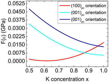
Figure 7. Calculated elastic strain energy density F(ε) of KxNa1−xNbO3 thin films grown on (110) NdScO3 substrates as a function of the film composition x (x = 0.5−1). Thereby the two different surface orientations—(100)pc (red curve) and (001)pc (blue and cyan curve)—have to be considered.
In order to verify our theoretical predictions, K0.9Na0.1NbO3 thin films were epitaxially grown on (110) NdScO3 (NSO) substrates. The surface topology (not shown) of a 28 nm K0.9Na0.1NbO3 epitaxial thin film is rather smooth with an rms roughness well below 0.5 nm. The piezoresponse force micrographs recorded in the same region reveal a rather complex ferroelectric domain structure. In the vertical amplitude image (Figure 8A), comparatively large domain bundles can be resolved. They are tentatively aligned along the [001]NSO direction with typical lateral sizes between 50 and 200 nm. The corresponding lateral amplitude image (Figure 8B) shows that the large domain bundles exhibit a prominent substructure consisting of a highly periodic array with alternating narrow and broad domains along [001]NSO. In this direction, the lateral period amounts to about 30 nm. In addition, these domain walls are very sharp and tilted off by about ±15° with respect to the [10]NSO direction. These domain wall angles can be also evaluated from the Fourier transform in the inset of Figure 8B.
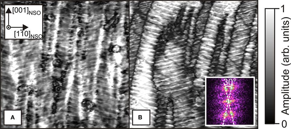
Figure 8. (A) Vertical and (B) lateral piezoresponse force microscopy amplitude images (1 µm × 1 µm) of a 28 nm thick K0.9Na0.1NbO3 film on (110) NdScO3 substrate.
In order to get in-plane structural information, GIXD has been performed. The in-plane reciprocal space maps in the vicinity of the (008)NSO (Figure 9A) and (24)NSO (Figure 9B) substrate Bragg reflections show a characteristic peak splitting (P1, P2), while the intensity distribution nearby the (40)NSO Bragg reflection exhibits a single peak only (not shown here). Similar to NaNbO3 films grown on TbScO3, these findings indicate an alternate in-plane shearing of the pseudocubic unit cells by β = ± 0.12° along the [001]NSO direction, while the crystal lattice remains coherent along the [1-0]NSO direction. Again, this verifies the existence of a1a2 domains that are (100)pc oriented a1a2 domains that exhibit exclusive in-plane polarization.
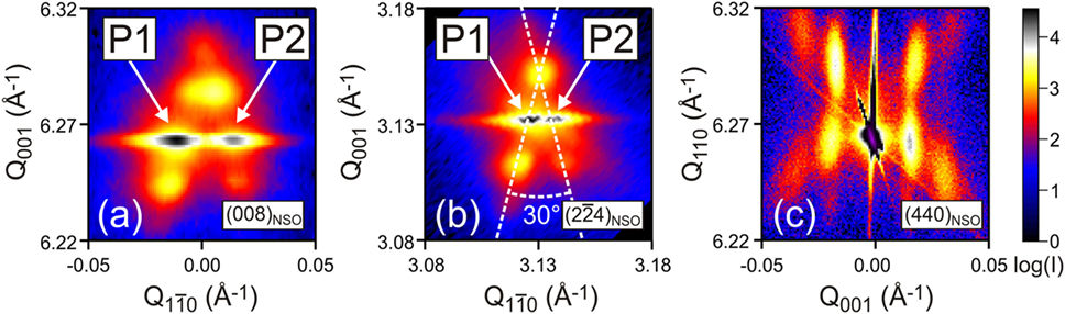
Figure 9. In-plane grazing incidence X-ray diffraction of the 28 nm thick K0.9Na0.1NbO3 film on (110) NdScO3 (NSO) substrate in the vicinity of the (008)NSO (A) and (24)NSO (B) substrate Bragg reflection. (C) Out-of-plane reciprocal space map in the vicinity of (440)NSO of the same film.
In order to identify a possible (001)pc thin film orientation, out-of-plane X-ray diffraction has been performed. The intensity distribution in the vicinity of the (440)NSO substrate Bragg reflection is illustrated in Figure 9C. The intensity distribution does not show a direct evidence of (001)pc domains. This is presumably caused by the small scattering volume as compared to the dominating large (100)pc domains. Nevertheless, the occurrence of equidistant satellite peaks in Figure 9C can only be explained, if a period arrangement of two orientations with different out-of-plane lattice parameters exists. Together with the alternating domain pattern determined in PFM, this strongly indicates the coexistence of (100)pc and (001)pc oriented phases, which are identified as a1a2 and MC domains, respectively (see Figure 10). A detailed analysis of the data is given in Schmidbauer et al. (2017).
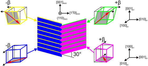
Figure 10. Model of the herringbone pattern in K0.9Na0.1NbO3 thin films on NdScO3 substrates exhibiting an interlaced a1a2 and MC domain structure.
The observation of a MC phase agrees with our predictions from the strain-phase diagram, which is calculated for a (001)pc oriented mono-domain. This is in contrast to r (or MA) domains, which would be expected from the strain-phase diagram derived by Bai and Ma (2010). The additional occurrence of a1a2 is plausible considering that, on the one hand, both MC and a1a2 domains exhibit the same unit cell with Pm symmetry and, on the other hand, they differ only in spatial orientation and are interconnected by 90° rotations (Bokov and Ye, 2004).
We conclude that according to our theoretical predictions both the monoclinic a1a2 and MC phases, arranged in a periodic, interlaced domain structure and with polarization discontinuities at each domain wall in [001]NSO direction, have been established for K0.9Na0.1NbO3/NdScO3. Hence, strong piezoelectric responses are anticipated for this material system. For estimating the piezoelectric coefficient of such K0.9Na0.1NbO3 thin films, we have grown them on SrRuO3/NdScO3, where the SrRuO3 intermediate film serves as bottom electrode. In order to prevent premature lattice relaxation, a thickness of 10 nm has been chosen for SrRuO3. Preliminary experiments have yielded a promising value of dzz = 29 pm/V for a 28 nm K0.9Na0.1NbO3 film, which is competitive with piezoelectric coefficients recorded for Pb(Zr,Ti)O3 thin films with similar thickness. Extended investigations on samples with bottom electrode are in progress.
Conclusion
The piezo- and ferroelectric properties of KxNa1−xNbO3 epitaxial films can be tailored by adequate application of lattice strain. In order to understand the underlying physical mechanisms, we have performed detailed calculations of (i) the strain-phase diagram within the framework of the LGD model and (ii) the strain energy density using linear elasticity theory. These calculations suggest that the structural and resulting ferroelectric properties of thin films critically depend on the film-substrate lattice mismatch, the film surface orientation, and the potassium atomic concentration. In this paper, we have discussed selected examples that are in full agreement with expectations from our theoretical considerations:
I. NaNbO3 thin films have been grown by the MOCVD technique on high-quality NdGaO3, SrTiO3, DyScO3, TbScO3, and GdScO3 substrates. Keeping this particular order, the incorporated lattice strain is systematically varied from compressive to tensile while the electrical polarization vector rotates from mainly vertical orientation to a pure in-plane alignment. Based on the calculated elastic strain energy density an exact prediction of the unit cell orientation can be made as first step for domain engineering.
II. For the selected case of tensely strained NaNbO3 films grown on ReScO3 substrates (Re = Dy, Tb, Gd), a well-ordered monoclinic a1a2 stripe domain pattern with pure in-plane polarization is observed. Increasing the film thickness leads to plastic relaxation and, thus, to a reduction of the in-plane lattice strain. As a consequence, MB domains with an additional vertical polarization component are formed.
III. On the basis of abovementioned calculations, a featured potassium concentration (x ≈ 0.9) of KxNa1−xNbO3 thin films grown on (110) NdScO3 substrate could be identified. This combination favors the coexistence of two equivalent, monoclinic, but differently oriented ferroelectric phases. We could indeed experimentally verify the existence of alternating (100)pc oriented a1a2 and (001)pc oriented MC monoclinic domains that are interlaced in a periodic herringbone structure. The coexistence of different types of ferroelectric domains leads to polarization discontinuities at the domain walls, enabling polarization rotation in the material, which is responsible for the very promising result for piezoelectric response of the film. The measured piezoelectric coefficient is comparable to those of lead-based oxide films with similar film thickness.
These examples demonstrate the principal ability to tune the structural and ferroelectric properties of epitaxial thin films by targeted incorporation of epitaxial strain. This could lead to a development of improved electronic applications, such as sensors, tunable microwave, and surface acoustic wave devices, on the basis of lead-free materials. However, for many technological applications the presence of an intermediate conducting layer on the bare oxide substrate serving as a bottom electrode would be mandatory. Therefore, extended investigations of samples containing a thin SrRuO3 layer are presently in progress.
Author Contributions
Piezoresponse force microscopy measurements and calculations of elastic strain energy density and strain-phase diagram were carried out by DB. MH and MS performed X-ray diffraction measurements and evaluation. MOCVD was realized by JS, while RU grew the perovskite oxide substrates. All authors participated in data analysis and manuscript writing.
Conflict of Interest Statement
The authors declare that the research was conducted in the absence of any commercial or financial relationships that could be construed as a potential conflict of interest.
Acknowledgments
The authors would like to thank A. Duk, A. Kwasniewski, J. Sellmann, H. Renevier, D. Novikov, D. Többens for assistance with the PFM and x-ray measurements and M. Klann and S. Markschies for MOCVD sample growth. We also thank DESY (project II-20080012), BESSY (project 14201208-ST), and ESRF (project MA-2233) for providing beam time. We are grateful to the bulk oxide group at the Leibniz Institute for Crystal Growth for providing us with high-quality rare-earth scandate substrates. The SrRuO3 bottom electrode layers have been deposited on NdScO3 substrate by A.S. Everhardt (University of Groningen).
References
Bai, G., and Ma, W. (2010). Phenomenological analysis of phase transitions in epitaxial perovskite ferroelectric thin films. Phys. B 405, 1901. doi: 10.1016/j.physb.2010.01.070
Bokov, A. A., and Ye, Z.-G. (2004). Domain structure in the monoclinic Pm phase of Pb(Mg1/3Nb2/3)O3–PbTiO3 single crystals. J. Appl. Phys. 95, 6347. doi:10.1063/1.1703830
Catalan, G., Lubk, A., Vlosswijk, A. G., Snoeck, E., Magen, C., Janssens, A., et al. (2011). Flexoelectric rotation of polarization in ferroelectric thin films. Nat. Mater. 10, 963. doi:10.1038/NMAT3141
Coh, S., Heeg, T., Haeni, J. H., Biegalski, M. D., Lettieri, J., Edge, L. F., et al. (2010). Si-compatible candidates for high-k dielectrics with the Pbnm perovskite structure. Phys. Rev. B 82, 064101. doi:10.1103/PhysRevB.82.064101
Damodaran, A. R., Agar, J. C., Pandya, S., Chen, Z., Dedon, L., Xu, R., et al. (2016). New modalities of strain-control of ferroelectric thin films. J. Phys. Condens. Mater. 28, 263001. doi:10.1088/0953-8984/28/26/263001
Davis, M., Budimir, M., Damjanovic, D., and Setter, N. (2007). Rotator and extender ferroelectrics: importance of the shear coefficient to the piezoelectric properties of domain-engineered crystals and ceramics. J. Appl. Phys. 101, 054112. doi:10.1063/1.2653925
Duk, A., Schmidbauer, M., and Schwarzkopf, J. (2013). Anisotropic one-dimensional domain pattern in NaNbO3 epitaxial thin films grown on (110) TbScO3. Appl. Phys. Lett. 102, 091903. doi:10.1063/1.4794405
Gruverman, A., Auciello, O., and Tokumoto, H. (1996). Scannning force microscopy for the study of domain structure in ferroelectric thin films. J. Vac. Sci. Technol. B 14, 602. doi:10.1116/1.589143
Guguschev, C., Galazka, Z., Kok, D. J., Juda, U., Kwasniewski, A., and Uecker, R. (2015). Growth of SrTiO3 bulk single crystals using edge defined film-fed growth and the Czochralski methods. Cryst. Eng. Comm. 17, 4662. doi:10.1039/c5ce00798d
Haertling, G. H. (1999). Ferroelectric ceramics: history and technology. J. Am. Ceram. Soc. 82, 797. doi:10.1111/j.1151-2916.1999.tb01840.x
Hammerschmidt, T., Kratzer, P., and Scheffler, M. (2007). Elastic response of cubic crystals to biaxial strain: analytic results and comparison to density functional theory for InAs. Phys. Rev. B 75, 235328. doi:10.1103/PhysRevB.75.235328
Koster, G., Kropman, B. L., Rijnders, G. H., Blank, D. A., and Rogalla, H. (1998). Quasi-ideal strontium titanate crystal surfaces through formation of strontium hydroxide. Appl. Phys. Lett. 73, 2920. doi:10.1063/1.122630
Lee, D., and Noh, T. W. (2012). Giant flexoelectric effect through interfacial strain relaxation. Phil. Trans. R. Soc. A 370, 4944. doi:10.1098/rsta.2012.0200
Liang, L., Li, Y. L., Chen, L.-Q., Hu, S. Y., and Lu, G.-H. (2009). A thermodynamic free energy function for potassium niobate. Appl. Phys. Lett. 94, 072904. doi:10.1063/1.3081418
Noheda, B. (2002). Structure and high-piezoelectricity in lead oxide solid solutions. Curr. Opin. Solid State Mater. Sci. 6, 27. doi:10.1016/S1359-0286(02)00015-3
Pertsev, N. A., Zembilgotov, A. G., and Tagantsev, A. K. (1998). Effect of mechanical boandary conditions on phase diagrams epitaxial ferroelectric thin films. Phys. Rev. Lett. 80, 1988. doi:10.1103/PhysRevLett.80.1988
Roitburd, A. L. (1976). Equilibrium structure of epitaxial layers. Phys. Stat. Sol. 37, 329. doi:10.1002/pssa.2210370141
Schlom, D. G., Chen, L.-Q., Eom, C.-B., Rabe, K. R., Streiffer, S. K., and Triscone, J.-M. (2007). Strain tuning of ferroelectric thin films. Annu. Rev. Mater. Res. 37, 589. doi:10.1146/annurev.matsci.37.061206.113016
Schmidbauer, M., Kwasniewski, A., and Schwarzkopf, J. (2012). High-precision absolute lattice parameter determination of SrTiO3, DyScO3 and NdGaO3, NdGaO3 single crystals. Acta Cryst. B 68, 8. doi:10.1107/S0108768111046738
Schmidbauer, M., Braun, D., Markurt, T., Hanke, M., and Schwarzkopf, J. (2017). Strain engineering of monoclinic domains in KxNa1-xNbO3 epitaxial layers: a pathway to enhanced piezoelectric properties. Nanotechnology 28, 24LT02. doi:10.1088/1361-6528/aa715a
Schmidbauer, M., Schäfer, P., Besedin, S., Grigoriev, D., Köhler, R., and Hanke, M. (2008). A novel multi-detection technique for 3D reciprocal space mapping in grazing incidence x-ray diffraction. J. Synchrotron. Radiat. 15, 549. doi:10.1107/S0909049508023856
Schmidbauer, M., Sellmann, J., Braun, D., Kwasniewski, A., Duk, A., and Schwarzkopf, J. (2014). Ferroelectric domain structure of NaNbO3 epitaxial thin films grown on (110) DyScO3 substrates. Phys. Stat. Sol. 8, 522. doi:10.1002/pssr.201409012
Schwarzkopf, J., Braun, D., Schmidbauer, M., Duk, A., and Wördenweber, R. (2014). Ferroelectric domain structure of anisotropically strained NaNbO3 epitaxial thin films. J. Appl. Phys. 115, 204105. doi:10.1063/1.4876906
Schwarzkopf, J., Schmidbauer, M., Remmele, T., Duk, A., Kwasniewski, A., Bin Anooz, S., et al. (2012). Strain induced phase transitions in NaNbO3 epitaxial thin films grown by metal-organic chemical vapor deposition. J. Appl. Cryst. 45, 1015. doi:10.1107/S0021889812035911
Setter, N., Eng, L., Fox, G., Gevorgian, S., Hong, S., Kingdon, A., et al. (2006). Ferroelectric thin films: review of materials, properties, and applications. J. Appl. Phys. 100, 051606. doi:10.1063/1.2336999
Soergel, E. (2011). Piezoresponse force microscopy (PFM). J. Phys. D Appl. Phys. 44, 464003. doi:10.1088/0022-3727/44/46/464003
Uecker, R., Klimm, D., Bertram, R., Bernhagen, M., Schulze-Jonack, I., Brützam, M., et al. (2013). Growth and investigation of Nd1-xSmxScO3 and Sm1-xGdxScO3 solid-solution single crystals. Acta Phys. Pol. A 124, 295. doi:10.12693/APhysPolA.124.295
Uecker, R., Velickov, B., Klimm, D., Bertram, R., Bernhagen, M., Rabe, M., et al. (2008). Properties of rare-earth scandate single crystals (Re=Nd-Dy). J. Cryst. Growth 310, 2649. doi:10.1016/j.jcrysgro.2008.01.019
Uecker, R., Wilke, H., Schlom, D. G., Velickov, B., Reiche, A., Polity, M., et al. (2006). Spiral formation during Czochralski growth of rare-earth scandates. J. Cryst. Growth 295, 84. doi:10.1016/j.jcrysgro.2006.07.018
Vailionis, A., Boschker, H., Siemons, W., Houwman, E., Blank, D. H., Rijnders, G., et al. (2011). Misfit strain accommodation in epitaxial ABO3 perovskites: lattice rotations and lattice modulations. Phys. Rev. B 83, 064101. doi:10.1103/PhysRevB.83.064101
Vanderbilt, D., and Cohen, M. H. (2001). Monoclinic and triclinic phases in higher-order Devonshire theory. Phys. Rev. B 63, 094108. doi:10.1103/PhysRevB.63.094108
Wang, J., and Zhang, T.-Y. (2005). Effects of nonequally biaxial misfit strains on the phase diagram and dielectric properties of epitaxial ferroelectric thin films. Appl. Phys. Lett. 86, 192905. doi:10.1063/1.1923765
Zembilgotov, A. G., Böttger, U., and Waser, R. (2008). Effect of in-plane shear strain on phase states and dielectric properties of epitaxial ferroelectric thin films. J. Appl. Phys. 104, 054118. doi:10.1063/1.2976347
Keywords: ferroelectric domains, KxNa1−xNbO3, thin films, strain engineering, epitaxial growth, X-ray diffraction, piezoresponse force microscopy, metal-organic chemical vapor deposition
Citation: Schwarzkopf J, Braun D, Hanke M, Uecker R and Schmidbauer M (2017) Strain Engineering of Ferroelectric Domains in KxNa1−xNbO3 Epitaxial Layers. Front. Mater. 4:26. doi: 10.3389/fmats.2017.00026
Received: 28 April 2017; Accepted: 31 July 2017;
Published: 16 August 2017
Edited by:
Daniel Schick, Helmholtz-Zentrum Berlin (HZ), GermanyReviewed by:
Joka Buha, IIT Genova, AustraliaGustau Catalan, Institució Catalana de Recerca i Estudis Avançats (ICREA), Spain
Copyright: © 2017 Schwarzkopf, Braun, Hanke, Uecker and Schmidbauer. This is an open-access article distributed under the terms of the Creative Commons Attribution License (CC BY). The use, distribution or reproduction in other forums is permitted, provided the original author(s) or licensor are credited and that the original publication in this journal is cited, in accordance with accepted academic practice. No use, distribution or reproduction is permitted which does not comply with these terms.
*Correspondence: Jutta Schwarzkopf, anV0dGEuc2Nod2FyemtvcGZAaWt6LWJlcmxpbi5kZQ==