 Bo Zhang
 Pu-Xian Gao
- Department of Materials Science and Engineering, Institute of Materials Science, University of Connecticut, Storrs, CT, United States
In recent years, engineered nanostructure assemblies such as nanowire arrays have attracted much research attention due to their unique chemical and functional characteristics collectively. The engineered nano-assemblies usually carry the characteristics distinct from bulk as a result of a size effect in their comprised elemental building blocks. The nanoscale size induced high surface-to-volume ratio is a fundamental attribute responsible for various chemical and physical properties required in various technologically important applications such as catalysts and sensors. This review article surveys the latest progress in engineered metal oxide nanostructure arrays, i.e., nanoarrays, for advanced chemical sensors' design and application. It starts with an overview of gaseous chemical sensors followed by surveys of various fabrication methods and routes for metal oxide nanoarrays. Different sensing modes and corresponding applications have been highlighted in the mixed gaseous chemical sensing, which provides new approaches and perspectives to meet the challenges of selective gas sensing, such as the cross-sensitivity and inter-correlation of multiple sensing signals.
Introduction
Ultrahigh surface area, low cost, and unique properties are the major merits for various ceramic based nanomaterials such as metal oxide thin films and nanoparticles. These nanomaterials have been extensively used for fabricating efficient sensors that can be used in various environmental and process monitoring, including combustion and emissions, petroleum refinery, and renewable energy technologies (Mani and Rayappan, 2015; Usha et al., 2015). Such an implementation need mainly stems from the increasing concerns on the environmental safety, energy security, and sustainability that require effective and efficient sensors to sense and control various environmental situations such as analyte concentration and speciation in real time.
As the first and foundational step, single sensors have been usually designed to measure individual analytes by identifying parameters or components in the form of either chemical signatures, or physical information. Lately, to add the functional complexity allowed toward achieving smart sensing, multiple sensors or multiple signals can be purposely bundled and integrated together in order to provide a measurement capability of multiple analytes or to obtain multi-facet and distributed measurement of a single analyte concurrently. For instance, it is known that physisorption and chemisorption of gaseous analytes could perturb the sensor material's intrinsic characteristics such as its electrical, dielectric, and piezoelectric properties (Hierlemann et al., 2000). Such changes may be measured in the form of various signals in response to some unique characteristics of different analytes and provide characteristic pattern signatures individually.
Meanwhile, much progress has been made in the past decades by researchers focusing at different material length scale ranging from bulk to miniaturized microscale, to atomic scale. The potential incorporation of multiple functions synergistically into a miniaturized sensing device or platform ultimately would allow additional functional merits such as light weight, ease for system integration, and improvement over structure, function, and programmability in general (Lafratta and Walt, 2008; Jonjic et al., 2015; Ayerden and Wolffenbuttel, 2017; Zilberstein et al., 2017). It is noted that the surface or interfacial reactions usually play a critical role in gas sorption and related gas sensing process (Wang D. et al., 2009; Wang G. et al., 2012). As such, to obtain better sensitivity or detection limit, sensing materials with smaller size would be advantageous to ensure larger surface exposure or access to analytes, and result in higher device sensitivity for various gas sensors (Wang et al., 2004; Star et al., 2006; Lin et al., 2016; Xu et al., 2018). However, conventional random assemblies of nanoparticulates such as thick film or thin film are often thermally unstable and tend to aggregate at high temperature. Therefore, constructing ordered architectures by growing nanostructures in isolated forest fashion such as the geometrically defined nanoarrays could effectively address the thermal stability issue (Wu et al., 2011; Shim et al., 2012; Wang W.-N. et al., 2012). In fact, nanoarrays have been widely studied due to its excellent physical and chemical characteristics associated with the sensing functions, and it continues to be the forefront of sensor materials technology as a result of various needs mentioned earlier toward system integration and utilization (Iijima, 1991). As the material base, large-scale nanoarrays have been successfully prepared using various physical and chemical methods and widely applied in many sensing devices (Hong et al., 2001; Rabin et al., 2003; Xia et al., 2003, 2011; Piao et al., 2005). For example, arrays of metal oxide nanostructures in the form of one-dimensional (1D) or two-dimensional (2D) morphologies, could provide various benefits for sensing applications, ranging from mitigation of aggregation (Li and Wang, 2009; Zhang et al., 2015), facilitation over electron transfer (Ozoemena et al., 2008; Zhu et al., 2015), to stabilizing sensing performance (Zhang et al., 2010, 2012). In addition, the unique array structure allows control of population of accessible active sites and tailoring of compositions, size, and morphology. With decoration of catalytic nanoparticles or piezo-responsive components, nanoarray based sensors could display superb sensitivity, self-sufficient capability, as well as multiplication of sensor operation modes (Cao et al., 2006; Li et al., 2008; Xu et al., 2008; Wang G. et al., 2009).
In the past couple of decades, various nanoarrays based sensing materials have been studied, including carbon nanotubes (CNTs) (Li et al., 2003; Sotiropoulou and Chaniotakis, 2003; Star et al., 2006; Yang et al., 2010), metal oxide nanowire arrays [e.g., ZnO (Wang et al., 2006), TiO2 (Lu et al., 2008), CuO (Liao et al., 2009), MnO2 (Wang et al., 2018), Ga2O3 (Lin et al., 2016), and Fe2O3 (Xiong et al., 2013)], silicon nanoarrays (Kwon et al., 2018) III-V or II-VI based hetero-nanoarrays (Zhang et al., 2002), as well as the hybrid nanoarrays using multiple structures (Zang et al., 2014). These nanoarray sensing materials can promote sensing performance dramatically, however, the reviews exclusively on the nanoarray based chemical sensors are still limited, especially on the multi-component sensings, and corresponding sensing mechanisms. Apart from a necessary overview of the latest gas sensors developed based on a wide variety of nanoarrays, the comparison and evaluation of the multiple sensing modes and corresponding mechanisms are also needed to help clarify and possibly define the future directions of nanoarray sensor technology.
Herein this review will provide a timely survey on the main synthesis strategies and characterization of nanoarray sensors. The nanoarray based chemical sensors will be elaborated in different sensing modes or different sensing signals, and their sensing mechanisms. Subsequently, the discussion on the correlations between sensing signals and signal processing, and the associated gas cross-sensitivity and selectivity will be discussed. Finally, the latest development and future directions are summarized in metal oxide nanoarray based chemical sensors.
Nanoarray Chemical Sensor Design, and Fabrication Methods
Chemical Sensor Device and Materials Design
The research activity in the field of chemical and bio-sensing is currently directed toward highly sensitive and selective sensing materials, and to the new device structure design that is capable of different working modes and allows subsequent pattern recognition and multi-component analysis (Hagleitner et al., 2001). Based on the detectable signals, the sensing mechanisms applied in a nanoarray chemical sensor could be categorized into a few different modes, such as resistance-metric, impedance-metric, capacitance-metric, potentiometric, surface acoustic wave, and light irradiation mode that may include some optical modes as well as photo-assisted mode, and piezoelectrical mode. Resistive type sensor, the most extensively adopted strategy, measures inherent resistance that can be modulated by the chemisorption or absence of analytes. A typical chemo-resistive device would include a sensing material component and the interdigitated electrodes, as shown in Scheme 1A (Fleischer and Meixner, 1998). In the resistor-type sensors, the surface adsorption and desorption of the target gases are normally detected on the sensing materials through the induced surface and bulk electronic or electronic-ionic transport property changes. The most commonly used binary semiconductor metal oxides, such as SnO2, TiO2, and ZnO, could handle the temperature range up to 700°C, above which the materials stability becomes an issue. Recently, some other semiconducting metal oxides, including CeO2, Ga2O3, LaFeO3, and NiO, have promised as new resistive sensing materials for a higher temperature range between 700 and 1200°C (Gerblinger et al., 1995; Bene et al., 2001; Grudin et al., 2002; Ogita et al., 2003; Lantto et al., 2004; Fergus, 2007; Fleischer, 2008; Liu et al., 2008). However, with most of them being sensitive to the reducing gases such as CO, H2, and HCs, the cross-sensitivity is an issue directly relevant to the selectivity problems. Meanwhile, mesoporous oxide filters based on AlVO4, Ga2O3, and SiO2 have been designed as an efficient catalytic window for mitigating the non-specific bindings and allowing better analyte specificity (Fleischer et al., 1996, 2000; Leyer et al., 1997; Fleischer and Meixner, 1998; Fleischer, 2008).
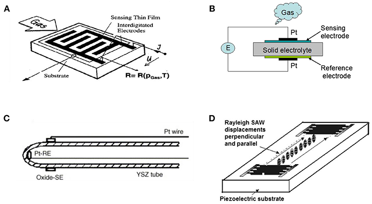
Scheme 1. (A) Typical structure of resistor-type gas sensors with interdigitated electrode. Reprinted with permission from Fleischer and Meixner (1998). copyright 1998 Elsevier B.V. (B) Schematic illustration of planar potentiometric gas sensor. (C) Schematic illustration of tubular YSZ impedance-metric sensor. Reprinted with permission from Nakatou and Miura (2006). copyright 2006 Elsevier B.V. (D) The Rayleigh SAW sensor excited by interdigital transducers, where displacements are parallel and perpendicular to the substrate surface. Reprinted with permission from Jakubik (2011). copyright 2011 Elsevier B.V.
The other design is potentiometric gas sensing, which measures the cross-electrolyte potential difference upon gas exposure where a solid electrolyte provides the electromotive force across the reference electrodes and sensing electrodes (Scheme 1B). The signal used to determine the concentration of analytes is measured as the potential difference between the working electrode and the reference electrode, with the working electrode's potential determined by the analyte concentration. Solid electrolyte based potentiometric gas sensors have been extensively studied for high temperature environment. High-temperature sensors for in situ and real-time environment monitoring are often based on electronic, ionic, or mixed ionic-electronic conductors. Pure ionic conductors are used in potentiometric, mixed-potential, or ampere-metric sensors, but electronic, and mixed (ionic–electronic) conductors are used in resistor-type sensors.
A typical fabrication route of the impedance-metric sensor is depicted in Scheme 1C. Firstly, the target gas analytes may adsorb, dissociate, and diffuse on the surface of working electrode, followed by charge transfer or ionic transport across grain boundaries. At various frequencies, some of these processes may contribute to the characteristic impedance response which is determined by the characteristics of the electrochemical cell or analyte species. Thus, the interfacial impedance is highly dependent on the adsorption of gaseous analytes onto sensing electrode while the variation in either electrolyte or sensing electrode would lead to the response of interface impedance change.
Scheme 1D illustrates a typical surface acoustic wave (SAW) based gas sensor design. For surface acoustic wave device, the majority of acoustic energy is concentrated near the surface and it makes SAW highly sensitive to any change of the physical or chemical properties (Achhab and Schierbaum, 2016). Thus, the adsorption of gas molecule will accordingly change boundary conditions for the surface waves, while the velocity and attenuation of the wave will also undergo a consequent change (Jakubik, 2011).
Fabrication Methods for Metal Oxide Based Nanoarrays
Hydrothermal Deposition Method
The hydrothermal route, which typically involves the use of chemical based aqueous solution for hydrolysis and precipitation reactions, is a conventional wet chemical method to synthesize nanomaterials such as nanoarrays immobilized on various shaped substrates such as two-dimensional (2D) planar and three-dimensional (3D) honeycomb ones. A typical hydrothermal method can be laid out with two steps, seed deposition, and hydrothermal growth. Sometimes deposition of seeds could facilitate the nucleation and growth of nanoarrays on substrates. The formation of nanoarrays is usually affected by experimental parameters such as pH value, concentration, temperature, and reaction time. Overall the hydrothermal synthesis method has proved to be a facile, cost-effective, and highly efficient approach to grow the various metal oxide nanostructures in a large scale, while the temperature, precursor concentration, and reaction time may have a great impact on the resultant nanostructure morphology, geometry, and distribution.
An example schematic illustration of a hydrothermal deposition process was displayed in Figure 1a (Chen et al., 2013). The reaction was carried out using Zinc Sulfate Heptahydrate (ZnSO4·7H2O) and Ammonium Chloride (NH4Cl) as the precursor in a bath of aqueous solution. A 2D ITO glass substrate with ZnO seed layers was immersed in the as-prepared precursor aqueous solution at 60°C for 45 min. Figures 1b,c depict the resultant morphology and structure of synthesized ZnO nanowire arrays after this process. Similarly, Lin et al. (Lin et al., 2016) have successfully utilized hydrothermal method to synthesize β-Ga2O3 nanorod arrays. The as-grown GaOOH nanowire arrays displayed in the Figures 1d,e possess a uniform structure in terms of shape and size. The concentrations of precursors usually play a critical role in the nucleation and growth of the hydrothermally grown nanostructures, leading to various geometrical distributions. For example, through adjusting lanthanum chloride (LaCl3·6H2O) concentration, Gao et al. (2016) successfully synthesized highly ordered double layered La doped SnO2 nanorod arrays with different crystallite size. The formation of La2Sn2O7 may alter the surface and increase crystallite size, with the three at % La-SnO2 possessing the highest ordered and large area double layered nanoarrays. Meanwhile, temperature, and reaction time also have a significant impact on growth outcomes such as nanostructure morphologies and the alignment in TiO2 nanoarrays (TNAs) (Li et al., 2010), as shown in Figure 1f, as synthesized using a 0.05 M TiCl3 precursor. The impact of temperature on the diameter and length has been summarized in Figure 1g, indicating that a higher temperature can greatly promote the nucleation and growth of TiO2. On the other case, the CeO2 nanowire arrays could also be obtained through a facile composite-hydroxide-mediated route reported by Zhang et al. (2007) This method is based on the reaction of source materials in a solvent of eutectic composite-hydroxides, providing a one-step, convenient, low-cost, nontoxic, and mass-production route.
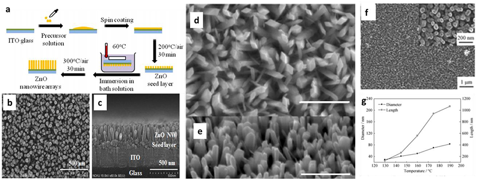
Figure 1. (a) A schematic of synthesis process of the ZnO nanowire arrays on the ITO glass substrate. The SEM images of ZnO NW arrays from (b) top view and (c) lateral view. Reprinted with permission from Chen et al. (2013). copyright (2013) Optical Society of America. (d) SEM image of GaOOH nanowires of (d) Top-view and (e) 45° tilt-view GaOOH nanowires grown at 150°C. All scale bars are 1 μm. Reprinted with permission from Lin et al. (2016). Copyright (2016) American Chemical Society. (f) SEM images of Titanium Dioxide Nano Arrays (TNAs) and localized high-magnification region is attached in the inset figure. (g) The trend of diameter and length vs. temperature of hydrothermal reaction. Reprinted with permission from Li et al. (2010). copyright 2010 the Nonferrous Metals Society of China and Springer-Verlag Berlin Heidelberg.
It is worth pointing out that all these above-mentioned examples are based on planar sample surface or 2D surface deposition, where mass transport issue will not be considered in general. However, when considering non-planar surface or 3D surface, the typical batch based static hydrothermal growth method would be prevented by the difficulty of mass transport within confined 3D space, resulting into the poor coverage of nanoarrays throughout the deposition substrate (Chen and Yin, 2012; Liu et al., 2014). A typical hydrothermally based continuous flow synthesis (CFS) method has been reported by Wang et al. (2017) to synthesize uniform ZnO nanorod arrays on 3-D honeycomb substrates. Multiple merits have been enabled, including low cost, high growth efficiency, and the ease for scalable integration. The growth schematic is depicted in Figure 2A. The corresponding SEM images of ZnO nanorod arrays grown using a batch process are shown in the Figures 2B–D. The ZnO nanowire arrays in the channel end area possess good alignment and uniform distribution but poor array density and randomly distributed precipitates was observed in the middle area of the channels. In comparison, significantly improved uniformity and alignment were obtained by using the CFS method according to the SEM observation shown in Figures 2E–G. Thus, the continuous flow-assisted synthesis would be beneficial for promoting mass transport in a confined space, which features significantly enhanced nucleation and growth rate of nanostructure deposition on the honeycomb substrates.
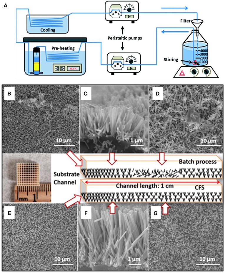
Figure 2. (A) Experimental setup of the continuous flow growing method. SEM images of typical ZnO nanoarray obtained from batch process: (B) top view and (C) cross-sectional view of channel end, and (D) top view of middle area; ZnO nanoarray achieved by CFS: (E) top view and (F) cross-sectional view of channel end, and (G) top view of middle area. Reprinted with permission from Wang et al. (2017). copyright 2017 The Royal Society of Chemistry.
Electrodeposition
In addition to hydrothermal method, the electrodeposition is also widely adopted in nanostructure growth, which deposits the materials onto a conductive surface from a solution containing the corresponding salts. The main advantage of electrodeposition method is conformal coating of nanostructure deposition regardless of the surface geometry of substrates. Even the top corner or the concave could be covered by a layer of the same thickness as that on the surface. But this technique always requires a relatively conductive substrate and thus limits its application in growing nanostructure on semiconductor or polymer substrate.
An electrochemical deposition of ZnO nanospike arrays on ITO glass was demonstrated by Debabrata et al. (Pradhan et al., 2009) Figures 3A,B revealed that the nanospikes in the form of global bunches and individual spike possess hexagonal trunks. Li et al. (2013) found that the initially pulsed potential could play a significant role to facilitate the growth of ZnO nanorod arrays on FTO glass substrate. As depicted in Figure 3C, a heterogeneous distribution accompanied with a sparse deposition was observed in the synthesis without employing initial pulses. In the contrast, when using initial voltage, ZnO nanorod arrays were achieved with a better morphology and more uniform size distribution, as illustrated in Figures 3D–F. It seems that the initial voltage pulse would be an important parameter to facilitate fast nucleation of ZnO nanoarrays. For the synthesis of CeO2 nanorod arrays on FTO substrate, a triple electrode setup was proposed by Younis et al. (2013) using which well aligned CeO2 nanorod arrays were achieved with a diameter of about 200 nm and rather smooth tip surfaces as displayed in the (Figure 3G). When doped with 5 and 10% Co, the diameter of nanorod was reduced to ~115 nm with coarse tips as shown in Figures 3H,I.
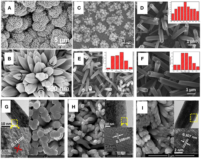
Figure 3. (A) Top view SEM image of nanospikes and (B) magnified images of nanospike arrays. Reprinted with permission from Pradhan et al. (2009). copyright 2015 IOP Publishing. SEM images of (C) ZnO by 1.5 h electrodeposition without initial pulse and ZnO nanoarrays with 0.1 s initial pulse for (D) 0.5 h, (E) 1.5 h, and (F) 3 h. The insets show the diameter distribution of ZnO rods. Reprinted with permission from Li et al. (2013). copyright 2013 Elsevier B.V. SEM images of as-synthesized (G) pure CeO2, (H) 5% Co doped, and (I) 10% Co doped CeO2 NRs on FTO substrate. Reprinted with permission from Younis et al. (2013). copyright 2013 AIP Publishing LLC.
Chemical Vapor Deposition
Chemical vapor deposition (CVD) is a vapor phase deposition process in which the desired material is produced by surface exposure and reaction of gaseous precursors on the deposition substrate. Such a process usually requires the precise control of various parameters such as temperature, pressure, precursor concentration. Depending on the pressure range, a CVD process can be classified as low pressure (~atmospheric pressure to 10−3 Torr) and high vacuum processes (~10−8-10−3 Torr). It has been widely employed to fabricate high crystallinity and less-defective nanoparticles, dense coatings, and films, as well as porosity-controlled films. In comparison to traditional hydrothermal method, the CVD often possesses relatively higher deposition rates. Besides a large variety of materials that can be deposited by CVD process, the target materials could be deposited with high purity due to the ease of removing impurities from gaseous precursors. Its major disadvantages come from the properties of the precursors and reactions. For example, sometimes CVD process could produce a number of toxic or corrosive byproducts, such as CO, H2, and HF.
At present, growing catalyst free or seed-free nanoarrays directly on a substrate surface is still a challenge up to now despite their scientific significance and application importance. Xu et al. (2015) reported a facile method to grow single-crystalline ZnO nanowire arrays in a large scale directly on a SiO2 substrate through CVD approach without involving any catalytic metal deposition or seed layers. An as-prepared Si substrate was etched to carve out the spikes and valleys firstly shown in Figures 4A,B. Then the ZnO nanoclusters would form and act as the nucleation sites (Figure 4C) and the subsequent growth of ZnO nanowires would sprout from the nucleation sites as shown in Figure 4D. ZnO nanowire arrays were achieved with a uniform size and morphology distribution, as illustrated in Figure 4E. No metal catalyst particle was revealed on the nanowire tips (Figure 4F). The length of ZnO nanowire could reach as high as 40 μm after 30 min growth (Figure 4G), with a preferential growth direction along [001], as determined in Figure 4H.
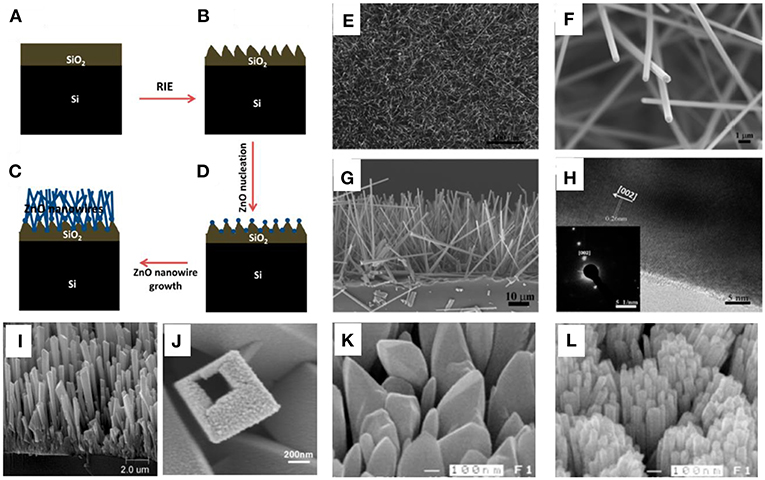
Figure 4. Schematic diagram of the growth process of ZnO nanowire array: (A) the pristine SiO2/Si substrate before etching; (B) Roughened SiO2/Si substrate surface with spikes and valleys; (C) ZnO nucleation sites on the RIE etched SiO2/Si substrate after etching treatment; (D) ZnO nanowire arrays grown from the ZnO nucleation sites. (E) Top view SEM image of the ZnO nanowires array; (F) Magnified SEM image of ZnO nanowires with clean and hexagonal tips. (G) Side view SEM image of a ZnO nanowire array. (H) HRTEM image of a single ZnO nanowire and the inset figure is the corresponding SAED pattern which indicate the growth direction is [001]. Reprinted with permission from Xu et al. (2015), copyright 2015 American Chemical Society. Microscopic figures of SnO2 tubes synthesized at 1,150°C: (I) cross-sectional view; (J) a single tube with partially opened top end. Reprinted with permission from Liu and Liu (2005), copyright 2005 WILEY-VCH Verlag GmbH & Co. KGaA, Weinheim. Morphologies of WO3 nanorod arrays synthesized at different temperatures: (K) 600°C, (L) 700°C. Reprinted with permission from Lu et al. (2010), copyright 2010 AIP Publishing LLC.
Liu and Liu (2005) reported a simple combustion assisted chemical vapor deposition (CVD) process to synthesize well aligned SnO2 nanoarrays with high yield. The vertically aligned nanoarrays were shown in Figure 4I. The individual SnO2 nanostructure was revealed as a “solid” rod with a square or rectangular cross section. A magnified observation in Figure 4J indicated an actually hollow inside. In addition, a facile means was developed by Lu et al. (2010) in 2009 to deposit ordered WO3 nanoarrays using a process of catalyst- and template-free hot filament chemical vapor deposition (HFCVD). The temperature would a key factor in controlling the morphologies. The growth at 600°C (Figure 4K) revealed the formation of irregular shaped nanostructure, while uniform WO3 nanoarrays were grown with an average length of about 1 μm at 700°C (Figure 4l).
Template-Assisted Method
Above mentioned methods have worked well when the chemistry can be readily tailored toward oriented growth and formation of dimensionally-anisotropic array structures. But when there is a lack of direct route for growing oriented nanostructures on solid surfaces, a template-assisted method has been effective and convenient approach for fabrication of nanoarrays. Two popular templates stand out historically, one is the anodized aluminum oxide (AAO) membrane, the other being polycarbonate track-etch membrane (Penner and Martin, 1987; Martin, 1994, 1996) Through template-assisted approach, both size and structure periodicity could be regulated, and to a good extent precisely controlled.
The fabrication of alumina template is usually a two-step process; by adjusting time, anodization potential, and the electrolyte solution composition, pores with different length and diameter could be generated (O'sullivan and Wood, 1970; Masuda and Fukuda, 1995; Li et al., 1999). Sander et al. (2004) reported a facile fabrication method assisted by AAO template to produce uniform and dense arrays of TiO2 nanoarrays with well-controlled dimensions directly on silicon substrates. As shown in Figure 5A, titania nanoarrays were deposited via ALD onto the AAO template with tunable ordered pores. The nanotube outer diameters were determined by the pore diameters in the alumina templates while heights of the nanotube equal to the thickness of the alumina films after a total filling (Figures 5B,C). The patterned growth of ZnO nanoarrays could facilitate the ability to control the position, size, and density of nanostructures precisely. The fabrication process of patterned masks designed by Greyson et al. (2004) is plotted in Figures 5D,E, the circular, catalytic gold areas of small diameters were formed in ordered square, hexagonal, and rectangular arrays through two positive-tone photoresists. It is revealed that arrays of ZnO nanowire only grew on the squared (Figure 5F), hexagonally (Figure 5G), and lined (Figure 5H) gold dots with different lengths depending on the growth conditions.
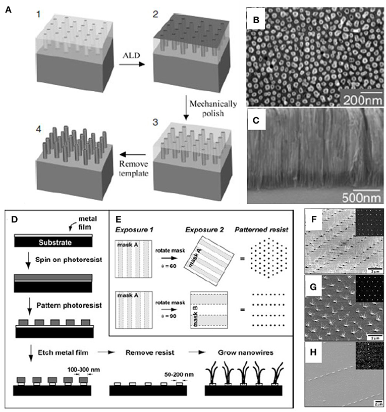
Figure 5. (A) Illustration of creating Titania nanotube arrays on substrate. The SEM images of (B) Top view and (C) side view of nanotubes. Reprinted with permission from Sander et al. (2004), copyright 2004 WILEY-VCH Verlag GmbH & Co. KGaA, Weinheim. The patterning of (D) catalytic gold dots and (E) photoresist posts with different shape and ordering. SEM images of ZnO nanowires arrays grown in (F) square lattice, (G) Hexagonal lattice, and (H) rectangular lattice. Reprinted with permission from Greyson et al. (2004), copyright 2004 WILEY-VCH Verlag GmbH & Co. KGaA, Weinheim.
Most of the reported works focus on synthesizing single component nanomaterials, growing well-aligned the binary or multiple components, i.e., heterogeneous nanostructure-assembly in a large scale is still a challenge. To meet this challenge, a new concept based on AAO template has been proposed by Wen et al. (2017, 2018) to design and fabricate binary heterogeneous architecture arrays by utilizing binary-pore anodized aluminum oxide template, which could precisely control size, morphologies, and heterogeneous pattern. A schematic of the fabrication process for a binary-pore template is depicted in the (Figure 6A). Using an imprinting process (Wen L. et al., 2014; Wang et al., 2016), an array of square pores were fabricated on the top and round pores were formed in the bottom. binary 1D nanostructure arrays could be generated with the assistance of the binary-pore template and the arrangements include nanowire/nanowire (Figure 6B), nanowire/nanotube (Figure 6C), nanotube/nanotube (Figure 6D), as obtained by electrodeposition and atomic layer deposition using the binary templates. In addition, a binary zero-dimensional (0D) Au nanodot/Ag nanodot arrays (Figure 6E) could also be fabricated through a physical vapor deposition (PVD) with the alumina template assisted technique.
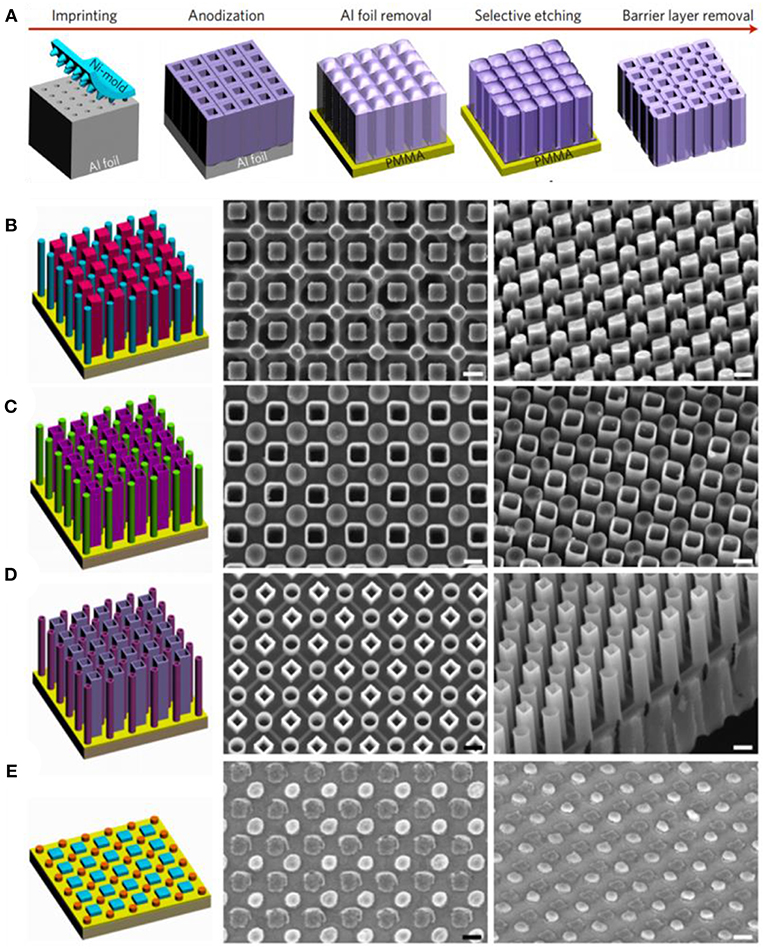
Figure 6. (A) Schematic diagram of fabrication process for a highly ordered porous alumina matrix template. Illustration and corresponding SEM figures: (B) nanowire/nanowire; (C) nanowire/nanotube; (D) nanotube/nanotube; (E) nanodot/nanodot. Scales are 200 nm. Reprinted with permission from Wen et al. (2017), copyright 2017 Macmillan Publishers Limited, part of Springer Nature.
Sensor Implementation of Metal Oxide Nanoarrays
Resistive Type Sensing Mode
The resistive mode is the most widely applied sensing mode. The chemical adsorption of oxidative or reducing analyte gases on semiconducting metal oxide may result in a thicker or thinner surface electronic depletion layer, which would increase or reduce the electrical resistance. Considering the nanoarrays are resistors with parallel or series connections depending on the electron transport routes, the variation of electrical resistance could quantitatively characterize the concentration of target gaseous analytes, such as NOx, SOx, O2, H2, and etc. The gas sensors based on 1D metal oxide nanostructures have been fabricated and demonstrated with enhanced gas sensing performance (Zhang et al., 2004; Wan and Wang, 2005). Vertically aligned nanorod arrays provide a simple matrix to study the electrical properties of assembled nanorods (Vayssieres et al., 2001; Lee et al., 2002; Park et al., 2002; Vayssieres, 2003). Cao et al. (2009) synthesized well-aligned and single crystalline WO3 nanowire arrays (Figure 7A) using a thermal evaporation approach. Fast and stable linear current-voltage (I-V) curve response and dynamic resistance-metric response are shown in Figures 7B,C, respectively, which suggest the formation of an Ohmic contacts in the interfaces and the detection limit could reach as low as 50 ppb range.
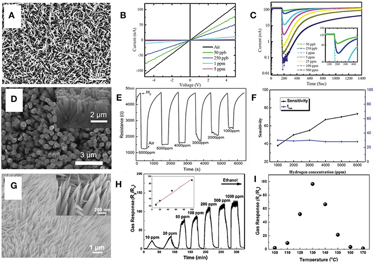
Figure 7. (A) Top view SEM images of a WO3-nanowire array. (B) IV curves of gas response to NO2 with different concentrations. (C) Dynamic resistance-metric response curves to NO2. Reprinted with permission from Cao et al. (2009), copyright The Royal Society of Chemistry 2009. (D) SEM images of Nb2O5 nanoarrays. (E) dynamic response to the different concentrations of H2; (F) The relationship of sensitivity and response time vs. H2 concentration; Reprinted with permission from Zou et al. (2018), copyright The Royal Society of Chemistry 2018. (G) Top view SEM images of Co3O4 nanoneedle arrays. (H) The dynamic response curve of the Co3O4 nanoneedle arrays to ethanol. The linear dependence of the gas response in the low concentration ethanol is attached in the inset figure. (I) The Temperature dependent gas response to ethanol. Reprinted with permission from Wen Z. et al. (2014), copyright 2014 Elsevier B.V.
H2 has been an important fuel and feedstock chemical in various processes for chemical production, food processing, metal refining, and electronics manufacturing. However, its inflammable and explosive nature demands the need in proper handling, monitoring, storage, and transportation (Hübert et al., 2011). As such, hydrogen gas sensor has been a critical asset in monitoring and controlling its concentration and leakage in various components and devices for H2 processing, storage, and transportation. A resistance-metric hydrogen sensor was fabricated using a facile hydrothermal catalyst-free method (Zou et al., 2018). The Nb2O5 nanorod arrays were grown using a hydrothermal method on a Nb foil (Figure 7D). An ultrahigh response of the sensor to hydrogen concentrations varying from 1,000 to 6,000 ppm were displayed in Figure 7E. The relationship of response time and sensitivity is summarized with respect to the H2 concentration, as illustrated in Figure 7F. The sensitivity toward H2 could be fitted into a linear curve as a function of H2 concentration while the response time was kept constant.
Among in ambient environment, volatile organic compounds (VOCs), such as benzene, acetone, and toluene, is a common part of the air contaminants that are detrimental to the environment and human health. Wen Z. et al. (2014) introduced a hydrothermally synthesized Co3O4 nanoneedle arrays for ethanol detection. The Co3O4 nanoneedle arrays have an average diameter of around 100 nm (Figure 7G). Upon injection of ethanol, the resistance undergoes a drastic enhancement and could generally recover to its initial value after the ethanol is released as shown in Figure 7H. Besides, the optimal working temperature for maximum response is determined to be 130°C according to Figure 7I. Besides, the SnO2 nanowire arrays is also reported as an excellent isopropanol sensor with enhanced sensitivity and selectivity (Zhao et al., 2018). The sensitivity of 1.5 at.% Sm-doped SnO2 nanoarrays toward 200 ppm isopropanol could reach as high as 78 and good selectivity was demonstrated toward other interfering VOCs gases.
Piezoelectrical Sensing Mode
In addition to the sensor device powered by external electrical source, a new mode of self-powered nanoarray gas sensor using piezoelectric effect has been developed, with some merits such as room-temperature detection, lower detection concentration limit, and lower energy consumption. Lin et al. (2014) introduced a ZnO nanowire piezo-nanogenerator (NG) as a self-powered active gas sensor that can detect reducing gas ethanol at room temperature. For the conventional resistance-metric gas sensor, a relatively high temperature (200~300°C) is required for activation of chemical sorption between ethanol and ZnO nanowire (Hsueh et al., 2007). In their work, the Pd nanoparticle has been incorporated to enhance the sensitivity (Figure 8a). Figure 8b indicates that the piezoelectric output of the Pd/ZnO nanoarray generator could serve as a power source, as well as a response signal to ethanol at room temperature as well. The device could be bent easily by fingers due to their flexible Kapton substrate (Figure 8c). The adsorption of ethanol may greatly change the piezoelectric properties and result into the variation of piezoelectric output voltage of the Pd/ZnO nanoarray (Figures 8d,e). In addition to metal/metal oxide hybrid structure, core-shell heterostructure could further enhance sensitivity. A typical In2O3/ZnO heterostructure nanoarrays self-powered gas sensor was designed by Zang et al. (2014) The Figure 8f illustrates the fabrication process of the In2O3/ZnO heterostructure nanowire arrays. The incorporation of In2O3 and resultant heterostructure interface would greatly facilitate the charge transfer upon exposure to H2S. Figure 8g exhibits that the sensitivity of In2O3/ZnO NWs is about seven times higher than that in pristine ZnO NWs, and the selectivity of In2O3/ZnO NW arrays against carbon disulfide, ethanol, methanol, formaldehyde, and acetone gases is summarized in Figure 8h. The sensitivity to H2S is overwhelmingly larger than that to interfering gases and a very good selectivity to H2S was achieved. Compared with resistance mode, the gas sensor based on piezoelectrical mode endow the device ability to function without external power source which reduce the energy consumption and simplify the electrode configuration. However, the concentration of target analytes could only be obtained with constant compressive force and thus sensing accuracy would be easily disturbed by fluctuation of compressive force in practical application.
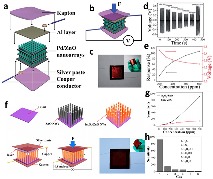
Figure 8. (a) Fabrication schematic of the self-powered active ethanol sensor based on Pd/ZnO nanoarray. (b) Electrical configuration and device structure of Pd/ZnO nanoarray. (c) The image displaying the flexibility of sensor device. (d) The dynamic piezoelectric response toward ethanol at room temperature. (e) The dependence of the sensitivity on the concentration of target analyte ethanol. Reprinted with permission from Lin et al. (2014), copyright the Royal Society of Chemistry 2013. (f) Fabrication protocol of the self-powered active gas sensor based on In2O3/ZnO nanowire arrays. (g) Comparison of sensing performance of In2O3/ZnO and pristine ZnO NW arrays upon exposure to H2S. (h) Selectivity histogram of the sensor upon exposure to 700 ppm of H2S and other interfering gaseous analytes at room temperature. Reprinted with permission from Zang et al. (2014), copyright 2014 American Chemical Society.
Saw Sensing Mode
The surface acoustic wave (SAW) is presumably operated through surface regions, as such it is usually very sensitive to surface perturbations such as mass loading, viscoelastic change, or electrical alternation. The wave signal transduced from the input electrical signal could be easily influenced by gaseous analytes, which may result into the change in amplitude, phase, frequency, and time-delay of output electrical signal (Ballantine et al., 1996). Such variation has been utilized to detect and measure the target gases (Cheeke and Wang, 1999). Thus, the gas sensor based on the SAW mode possesses various advantages such as high robustness, fast response, and good reproducibility. A novel SAW gas sensor based on Pt/ZnO nanorod arrays was realized by Huang et al. (2009) The major component of SAW sensor, the dual delay line system, is depicted in Figure 9A. The characterization of sensing materials is illustrated in Figure 9B. The mass of H2 on the surface per unit area may drive frequency decrease and measured frequency response is shown in Figure 9C. The sensitivity vs. concentration of hydrogen has been summarized in Figure 9D, where the response is defined as the difference between frequency under H2 and initial frequency. The frequency shift responds quickly toward lower concentration H2 but the response gradually saturates at large concentrations.
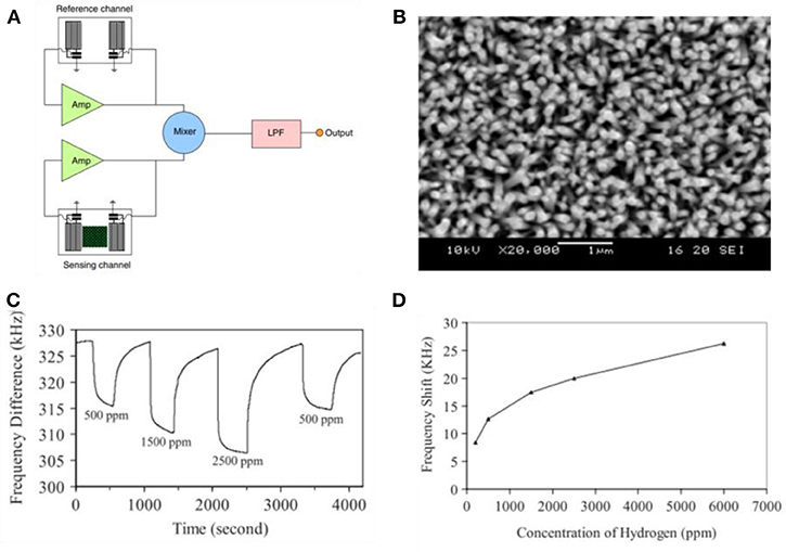
Figure 9. (A), Schematic diagram of a sensor fabrication. (B), SEM images of as prepared Pt/ZnO nanorod arrays. (C), The dynamic responses of the dual-channel sensor for different H2 concentrations. (D), Changes in frequency with H2 concentration. Reprinted with permission from Huang et al. (2009), copyright 2009 IOP Publishing Ltd.
Light Irradiation Sensing Mode
The photo illumination induced gas measurements could offer new opportunities to improve the sensor performance and decrease or expand the operating temperature windows. In fact, the optical sensing modes can easily prevail over the other methods with some outstanding merits, exemplified by the ability for non-contact and remote measurements. In the case of photocurrent based responses, the sensing response time could be as short as a small fraction of second (Zhou et al., 2009), and the selectivity could be very high as the photocurrent can be distinctly varied upon different chemical species exposure upon UV illumination. A photodetector based on gallium nitride (GaN) wide-bandgap semiconductor film and a light source using UV arc discharge lamp have been integrated to form an automotive exhaust gas sensor (Mello et al., 2006). The arc discharge lamp induces electronic transitions in the gas molecules flowing between the light source and the GaN photodetector. Such energy transitions modify the light in the UV spectral region which is quickly detected by the GaN photodetector as a function of exhaust gas concentration. By employing the luminescence due to probed gas adsorption, Faglia et al. (2005) revealed that the visible-band emission quench of SnO2 nanowires upon exposure to a few ppm of NO2, so was in the sensor made of porous silica shells of diatoms (Lettieri et al., 2008).
In the meantime, upon UV illumination, abundant electron-hole pairs may be generated in the ZnO and result in increasing concentration of either electrons or holes as the charge careers, and therefore resulting in sensing responses (Gogurla et al., 2014). The work by Lin et al. (2017) suggests that UV light could not only increase the sensitivity of resistance based nanoarray sensors, but also the response and recovery performance. The device testing setup is displayed in Figure 10a, where the as-synthesized Ga2O3 nanorod arrays were installed as the sensing elements on an Al2O3 ceramic substrate. These nanoarrays have a uniform diamond-shaped cross-section and a rod length of around 2 μm (Figure 10b). The typical dynamic sensing characteristics toward 100 ppm CO at 500°C with or without UV light are displayed in Figures 10c,d. UV light excitation raises the response speed by around 10% and accelerate recovery by 200 s due to the drastically increased concentration of free charge carriers. The enhanced room temperature gas sensing performance could also be realized by UV light irradiation and the effects of UV illumination on the response of SnO2-ZnO core-shell nanostructure was also investigated in the work reported by Park et al. (2013) The SnO2-core/ZnO-shell nanowires were synthesized via thermal evaporation and atomic layer deposition (ALD) and its morphology is presented in Figure 10d. The sensitivity is significantly enhanced due to the formation of heterostructure of SnO2 and ZnO in comparison to the pristine SnO2 and ZnO in room temperature NO2 sensing (Figure 10e). Besides, the Figure 10f demonstrates the sensitivity increased from 189 to 619% when UV intensity reached 1.2 mW/cm2. This improvement could be attributed to the enhanced NO2 adsorption and electron transfer promoted by UV illumination.
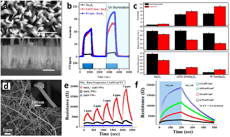
Figure 10. (a) Top view and lateral view SEM images of as-prepared Ga2O3 nanorod arrays. (b) The comparison of real-time CO gas sensing performance of pristine, LSFO decorated, and Pt-decorated b-Ga2O3 nanorod arrays. (c) Histogram of normalized sensitivity, recovery time, and recovery time with or without UV illumination tested at 500°C. Reprinted with permission from Lin et al. (2017), copyright 2017 AIP Publishing. (d) SEM images of SnO2-ZnO core-shell nanowires. (e) The comparison of dynamic response of SnO2-ZnO hybrid nanowires, pristine SnO2 nanowires, and ZnO nanowires under UV illumination at room temperature. (f) The dynamic response of SnO2-ZnO hybrid nanowires toward 5 ppm NO2 under UV irradiation with different intensities. Reprinted with permission from Park et al. (2013), copyright 2013 American Chemical Society.
Gas Mixture Analysis Using Multiple Sensor Devices
Quantitative analysis of multiple gases or a gas mixture has been a challenging goal despite the extensive work on gaseous chemical sensors in the past few decades, especially on the metal oxide semiconductor sensors. To enhance the selectivity and identify individual gas components from a gas mixture, an array of multiple gas sensors, i.e., gas sensor array, has been usually assembled to measure and analyze the targeted volatile chemical analytes. Such a sensor array gathers multiple sets of data through the respective individual chemical sensors, which would contain broadly overlapping sensitivity profiles. The substantial analysis of multiple sensing signals obtained from different sensor devices often involves a pattern-recognition method to differentiate the target analytes, a significant step toward developing a smart sensor array device named Electronic noses (E-noses) (Persaud and Dodd, 1982; Carpenter et al., 2012). The common computational methodologies employed to quantitatively analyze the response data for a sensor array include learning vector quantization (LVQ), principal component analysis (PCA), partial least squares (PLS), multiple linear regression (MLR), principal component regression (PCR), and discrimination function analysis (DFA) (Jurs et al., 2000; Pearce et al., 2006).
By extracting the pattern of different gas species from global responses, Chen et al. (2011) utilized PCA data processing to differentiate the air-diluted NO2, H2S, NH3. CO, and H2. The resistance-metric response was measured by ZnO nanowires decorated with SnO2 and noble metal nanoparticles (e.g., Pd, Pt, or Au), and the database was established based on their resistive sensitivities. PCA process could effectively reduce the dimensionality of the data-set by projecting these data points into a 2D plane and maintain the major information by using covariance analysis. The plot in two principal component spaces is illustrated in Figure 11A. When incorporated with the response rates of different gases, as displayed in Figure 11B, different gas species could be easily distinguished via their different response trends.
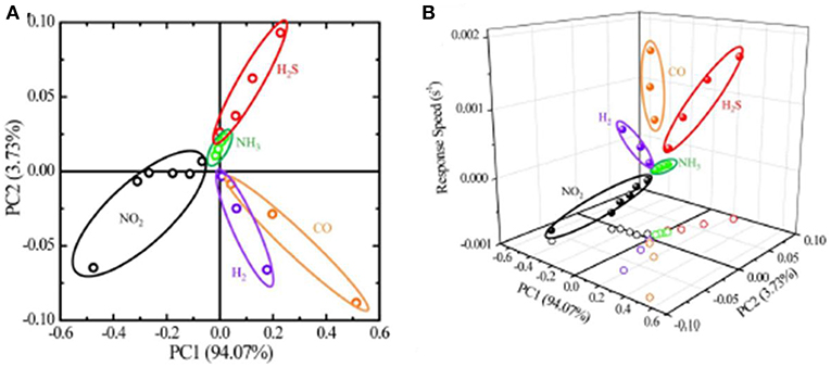
Figure 11. (A) The process dataset in a 2D plane after PCA analysis. (B) Processed PCA data after incorporating response speeds as an extra discrimination factor. Reprinted with permission from Chen et al. (2011), copyright 2010 IEEE.
Another effective design for sensor array has been proposed by Chen et al. (2018) who developed an E-nose by incorporating four electrodes (Pt, Ni, Au, and ITO) into one device (Figure 12a). The sensor system contains a read-out system, a wireless data transmission unit, a mobile phone receiver, and a data processing application as demonstrated in Figure 12b. The real-time response toward different gaseous analytes was measured using traditional resistance-metric mode individually and the sensitivity to individual gas analytes with various concentrations was summarized as a database. The training vectors were defined by the input data points extracted from this database, with each vector representing one gas species. The axes shown in Figures 12c,d represent the sensitivity of different gases, no overlap was observed between the sensitivity patterns of different analytes. When applying in practical gas detection, no overlap will be observed even if the identification zone of sensitivity is set at 3%.
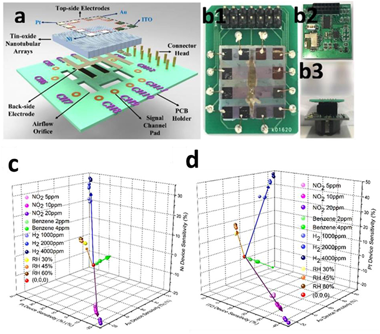
Figure 12. (a) Schematic of E-nose device fabrication. (b) Photograph of integrated circuit of sensor system. The 3D scatter plot (c,d) of gas classification in cubic maps through LVQ analysis. Reprinted with permission from Chen et al. (2018), copyright 2018 American Chemical Society.
The gas mixture detection has always been a challenging task, mostly due to the usually nonlinear relationship between responses and chemical concentrations, as well as the interaction (cross-talk) between the target gas analytes. Yang et al. (2015) proposed a simplified graphical method for a quick and easy quantitative analysis of multicomponent gas analytes. The multiplexed sensor array based on different sensing materials, consisting of CuO nanospikes, ZnO nanowires, and TiO2 nanotubes, was fabricated by a facile hybrid nanofabrication method (Figure 13A). The characteristic response curves of three sensing materials toward different combination of NO2 and CO mixture were extracted from the resistance-metric global responses while the concentrations of the gaseous components were determined by their intersections. However, three curves intersect with each other at three different points in practical application. The incenter of triangle was assumed and considered as the estimated concentration of NO2 and CO in the gas mixture (Figures 13B,C). The relative error of calculated concentration of NO2 and CO was determined to be 17.76 and 9.73%. It is noted the empirical approximation was used in this work, assuming the convergence is expected in the three gas responses upon mixing, may not be the case practically.
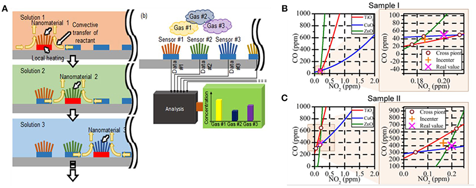
Figure 13. (A) Fabrication schematic of Heterogeneous Nanomaterial Array synthesized by Series of Localized Liquid-Phase method. Estimation of concentrations of NO2 and CO gases in sample gas I (B) and II (C). Reprinted with permission from Yang et al. (2015), copyright 2015 American Chemical Society.
Gas Mixture Analysis Using a Single Multi-Mode Sensor
As surveyed in section Gas Mixture Analysis Using Multiple Sensor Devices, enhanced selectivity could be achieved by combining artificial computational methods and multiple sensing signal datasets obtained from multiple sensor devices upon exposure to a gas mixture, a known concept of sensor arrays toward E-nose (Srivastava, 2003; Star et al., 2006). In such a sensor array, multiple target parameters could be detected simultaneously by providing characteristic signatures for individual analytes derived from the global responses of the building block sensors contained within the array. However, the commonly employed metal oxide nanoarray based multiple electrical sensors would require an external electrical power source and a number of robust electrical contacts, naturally adding the cost in device assembly, deployment, and operation energy usage. addition the other hand, the increasing number of deployed sensor devices may increase the risk of system malfunction as the increased complexity in electrical wiring, contact, and electrode interfacing could be a significant source to device degradation.
In fact, multi-dimensional patterns could be extracted from a single sensor output signal in a similar manner to those extracted from a multi-sensor array. As such, by correlating the characteristic signals obtained from multiple sensing modes subjected to a single sensor device would be a promising approach to realize a facile flow of device fabrication, deployment, and pattern-recognition. However, the reported work on multiple modes based nanoarray sensor has been rather limited so far. Llobet et al. (2001) correlated the direct current (DC) component and the first three harmonics of the Fourier Transform (FFT) analysis and Discrete Wavelet Transform (DWT) analysis to achieve multicomponent gas mixture detection using a single tin oxide gas sensor. The PCA results for the sensor responses processed by the FFT and DWT are displayed in Figures 14A,B. The separation between the measured species is good. Then the PCR and PLS-specialized models were built for the quantification of CO, NO2, and their binary mixture. Figure 14C shows that both PCR and PLS models could help estimate the concentrations of component gases.
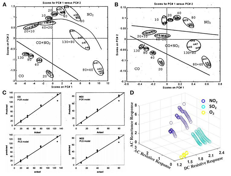
Figure 14. PCA plots of sensor response processed by the (A) FFT and (B) DWT method. (C) Predicted results vs. actual concentrations of CO and NO2 given by PCR and PLS models. Reprinted with permission from Llobet et al. (2001), copyright 2001 IEEE. (D) Preliminary 3D figure of correlated response dataset of impedance-metric and resistive modes for NO2, O2, and SO2.
However, the FFT and DWT analyses using original response data sets would be computationally complex and costly for a real-time gas detection. In the past decade, we have been working on multi-modular sensing using a single sensor device platform (Gao et al., 2012; Sun et al., 2014; Lin et al., 2017). The multicomponent gas detection has been achieved by correlating the signals of impedance-metric and resistive sensing mode of a single device. As shown in Figure 14D, a good separation of 2~4 ppm NO2, 30~50 ppm and 1,000~3,000 ppm O2 is achieved despite their similar resistive responses. Thus, the target analyte could be distinguished from an analyte mixture based on correlated dataset acquired through multiple sensing modes due to their unique physical and chemical interactions with metal oxide nanoarrays.
With the accumulation of multi-dimensional pattern information extracted from the output signals, the data-sets become much more complex for conventional data processing method to adequately deal with. Such a big data requires a set of techniques and technologies with new forms of integration and analysis in order to reveal specific insights from datasets which are diverse, complex, and of a massive scale (Hashem et al., 2015). Among the various analytical approaches, the Self Organized Map (SOM) has been proved to be an effective tool to complete the pattern recognition, as proposed by Ortega et al. (2001) As shown in Figures 15A,B, the presence of CO or CH4 is indicated by the responses, which however cannot be distinguished clearly. Thus, the traditional pattern recognition method failed to satisfy the selective analysis. The feature of pattern could be extracted from spectra analysis via Self Organized Map (SOM) paradigm (Figure 15C) and the trained SOM net is plotted in Figure 15D. This study presented a systematic work for selection of the best combination of analytical technologies or methods dealing with the static measures, dynamic response, and signal processing and it would be the key factor in systematically extracting the maximized information from global responses in the future development of multi-functional gas sensors.
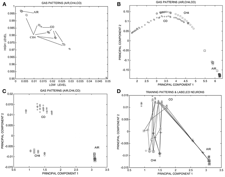
Figure 15. (A) Static measurement to CH4, CO, and air based on single sensor. (B) The projected image of gas patterns obtained from the output of one sensor heated with a triangular waveform. (C) The projected image of gas patterns obtained from FFT processing of the high temperature portion of the pulse heating waveform. (D) The projected image of SOM sub-nets and gas patterns, where three supervised SOM sub-nets are plotted. Reprinted with permission from Ortega et al. (2001), copyright 2001 Elsevier Science B.V.
Summary and Outlook
In conclusion, we have surveyed the latest progress on the development of the metal oxide based nanoarrays and their applications as sensing devices for various gaseous chemicals. The functional nanoarrays of various metal oxides could be synthesized using either template-free method or template-assisted strategy. The template-free syntheses have witnessed some fast growth of a selective group of metal oxide nanoarrays suitable for chemical sensing, such as ZnO, Ga2O3, TiO2, and In2O3, with their growth controlled by adjusting synthetic parameters such as the operating temperature and precursor concentration. In contrast, the template-assisted method could be more effective in adjusting morphology and size to a more precise extent, such as length, density, and diameter of nanostructures, as confined by the template geometry and pattern distribution. The patterned templates as a unique mask could also endow the ability to define the shape and the position of nanoarrays. Based on the nanoarrays with some typical characteristics such as high surface area, tunable size or morphology, and supreme physical and chemical functions, various chemical sensors have been demonstrated with superb performance for different target gaseous chemical detections.
Although significant achievements have been made on the nanoarray fabrication and sensor demonstration, several challenges remain worth tackling further in the near future, such as high energy consumption, low operating temperature window, cross-sensitivity, and etc. From the energy saving viewpoint, the operation temperature of metal oxide nanoarray based sensor is usually limited to a range of elevated or relatively high temperatures. As relatively less developed strategies, adoption of external light irradiation or embedded heater have been used to help locally activate the interaction of gases and nanoarrays, but it leads to increased energy consumption and inconvenience in the deployment. As such, the focus of sensor materials and devices should be continuously placed on further lowering the operating temperature especially for room temperature or low temperature detection, while expanding the operation temperature windows as necessary.
On the other hand, as an enabling device in measurement instrumentation and control, sensors that can operate under extreme environment have been technologically important for industrial process monitoring and control. Such sensor materials and related devices would usually involve harsh environment such as high temperature, high pressure, high erosion due to high flux and multiphase conditions, and high oxidative or reducing environments. Some example application scenarios include various fuel-fired and nuclear power plants, combustion engines and turbines, and oil field and petrochemical plants. Such extreme environments would demand the structural stability and functional stability in sensor materials and related interconnects and packaging components, besides the requirement of good sensitivity and selectivity under technically challenging conditions. The nanoarray based chemical sensors, if stand and work properly in the harsh environments, may be one of the promising solutions to help monitor and control various chemical feedstock and gaseous emission, enhance combustion and process efficiency, thus energy efficiency, and environmental sustainability.
In perspective of the sensing performance, the cross-sensitivity would be inevitable in practice, most of the reported gas sensors are single gas detectors as of now, and mixed gas detection has been traditionally achieved by assembling a series of different gas sensors as sensor arrays. As a new approach with good promises, multifunctional gas sensors can be designed with multiple working modes, and provide new data collection or even database that can be used to help improve sensing function in terms of accuracy, sensitivity, and selectivity. However, more in-depth studies are needed in this regard, as well as the clarification of the multiple gas detection mechanisms, which could improve the sensor working efficiency, and optimize energy efficiency, as well as big data input, processing, and utilization.
Finally, the development of multifunctional nanoarray sensing devices is expected to continue being targeted for ultra-high sensitivity, selectivity, stability, low energy consumption, and broad working temperature windows. Such smart sensing devices and systems may function as critical components in various precision manufacturing process control, perception modules of future humanoid AI robots, advanced battlefield monitors, and etc.
Author Contributions
P-XG: perceived and designed the review topic; BZ: drafted the manuscript; P-XG and BZ: revised and finalized the manuscript together.
Funding
The authors are grateful for the financial support from the US Department of Energy (Award Nos. DE-FE0026219 and DE-FE0011577) and the US National Science Foundation (Award No. CBET 1344792).
Conflict of Interest Statement
The authors declare that the research was conducted in the absence of any commercial or financial relationships that could be construed as a potential conflict of interest.
References
Achhab, M. E., and Schierbaum, K. (2016). Gas sensors based on plasma-electrochemically oxidized titanium foils. J. Sens. Sens. Syst. 5, 273–281. doi: 10.5194/jsss-5-273-2016
Ayerden, N. P., and Wolffenbuttel, R. F. (2017). The miniaturization of an optical absorption spectrometer for smart sensing of natural gas. IEEE Transac. Indus. Electron. 64, 9666–9674. doi: 10.1109/TIE.2017.2719600
Ballantine, D. Jr., White, R. M., Martin, S. J., Ricco, A. J., Zellers, E., Frye, G., et al. (1996). Acoustic Wave Sensors: Theory, Design and Physico-Chemical Applications. Amsterdam: Elsevier.
Bene, R., Pinter, Z., Perczel, I. V., Fleischer, M., and Reti, F. (2001). High-temperature semiconductor gas sensors. Vacuum 61, 275–278. doi: 10.1016/S0042-207X(01)00129-4
Cao, A.-M., Hu, J.-S., Liang, H.-P., Song, W.-G., Wan, L.-J., He, X.-L., et al. (2006). Hierarchically structured cobalt oxide (Co3O4): the morphology control and its potential in sensors. J. Phys. Chem. B 110, 15858–15863. doi: 10.1021/jp0632438
Cao, B., Chen, J., Tang, X., and Zhou, W. (2009). Growth of monoclinic WO 3 nanowire array for highly sensitive NO 2 detection. J. Mater. Chem. 19, 2323–2327. doi: 10.1039/b816646c
Carpenter, M. A., Mathur, S., and Kolmakov, A. (2012). Metal Oxide Nanomaterials for Chemical Sensors. New York, NY: Springer Science & Business Media.
Cheeke, J., and Wang, Z. (1999). Acoustic wave gas sensors. Sens. Actuat. B Chem. 59, 146–153. doi: 10.1016/S0925-4005(99)00212-9
Chen, J., Chen, Z., Boussaid, F., Zhang, D., Pan, X., Zhao, H., et al. (2018). Ultralow power smart electronic nose system based on three-dimensional tin-oxide nanotube arrays. ACS Nano. 12, 6079–6088. doi: 10.1021/acsnano.8b02371
Chen, J., Wang, K., and Zhou, W. (2011). Vertically aligned ZnO nanorod arrays coated with SnO2/noble metal nanoparticles for highly sensitive and selective gas detection. IEEE Transac. Nanotechnol. 10, 968–974. doi: 10.1109/TNANO.2010.2091423
Chen, L.-Y., and Yin, Y.-T. (2012). Facile continuous flow injection process for high quality long ZnO nanowire arrays synthesis. Cryst. Growth Design 12, 1055–1059. doi: 10.1021/cg201316f
Chen, M.-Z., Chen, W.-S., Jeng, S.-C., Yang, S.-H., and Chung, Y.-F. (2013). Liquid crystal alignment on zinc oxide nanowire arrays for LCDs applications. Optics Express 21, 29277–29282. doi: 10.1364/OE.21.029277
Faglia, G., Baratto, C., Sberveglieri, G., Zha, M., and Zappettini, A. (2005). Adsorption effects of NO 2 at ppm level on visible photoluminescence response of Sn O 2 nanobelts. Appl. Phys. Lett. 86:011923. doi: 10.1063/1.1849832
Fergus, J. W. (2007). Perovskite oxides for semiconductor-based gas sensors. Sens. Actuat. B Chem. 123, 1169–1179. doi: 10.1016/j.snb.2006.10.051
Fleischer, M. (2008). Advances in application potential of adsorptive-type solid state gas sensors: high-temperature semiconducting oxides and ambient temperature GasFET devices. Measure. Sci. Technol. 19:042001. doi: 10.1088/0957-0233/19/4/042001
Fleischer, M., Kornely, S., Weh, T., Frank, J., and Meixner, H. (2000). Selective gas detection with high-temperature operated metal oxides using catalytic filters. Sens. Actuat. B Chem. 69, 205–210. doi: 10.1016/S0925-4005(00)00513-X
Fleischer, M., and Meixner, H. (1998). Selectivity in high-temperature operated semiconductor gas-sensors. Sens. Actuat. B Chem. 52, 179–187. doi: 10.1016/S0925-4005(98)00271-8
Fleischer, M., Seth, M., Kohl, C. D., and Meixner, H. (1996). A study of surface modification at semiconducting Ga2O3 thin film sensors for enhancement of the sensitivity and selectivity. Sens. Actuat. B Chem. 36, 290–296. doi: 10.1016/S0925-4005(97)80084-6
Gao, F., Qin, G., Li, Y., Jiang, Q., Luo, L., Zhao, K., et al. (2016). One-pot synthesis of La-doped SnO 2 layered nanoarrays with an enhanced gas-sensing performance toward acetone. RSC Adv. 6, 10298–10310. doi: 10.1039/C5RA27270J
Gao, P.-X., Shimpi, P., Gao, H., Liu, C., Guo, Y., Cai, W., et al. (2012). Hierarchical assembly of multifunctional oxide-based composite nanostructures for energy and environmental applications. Int. J. Mol. Sci. 13, 7393–7423. doi: 10.3390/ijms13067393
Gerblinger, J., Lohwasser, W., Lampe, U., and Meixner, H. (1995). High-temperature oxygen sensor-based on sputtered cerium oxide. Sens. Actuat. B Chem. 26, 93–96. doi: 10.1016/0925-4005(94)01564-X
Gogurla, N., Sinha, A. K., Santra, S., Manna, S., and Ray, S. K. (2014). Multifunctional Au-ZnO plasmonic nanostructures for enhanced UV photodetector and room temperature NO sensing devices. Sci. Rep. 4:6483. doi: 10.1038/srep06483
Greyson, E. C., Babayan, Y., and Odom, T. W. (2004). Directed growth of ordered arrays of small-diameter ZnO nanowires. Adv. Mater. 16, 1348–1352. doi: 10.1002/adma.200400765
Grudin, O., Marinescu, R., Landsberger, L. M., Kahrizi, M., Frolov, G., Cheeke, J. D. N., et al. (2002). High-temperature gas sensor using perovskite thin films on a suspended microheater. J. Vacuum Sci. Technol. Vacuum Surf. Films 20, 1100–1104. doi: 10.1116/1.1463072
Hagleitner, C., Hierlemann, A., Lange, D., Kummer, A., Kerness, N., Brand, O., et al. (2001). Smart single-chip gas sensor microsystem. Nature 414:293. doi: 10.1038/35104535
Hashem, I. A. T., Yaqoob, I., Anuar, N. B., Mokhtar, S., Gani, A., and Khan, S.U. (2015). The rise of “big data” on cloud computing: review and open research issues. Inf. Syst. 47, 98–115. doi: 10.1016/j.is.2014.07.006
Hierlemann, A., Ricco, A. J., Bodenhöfer, K., Dominik, A., and Göpel, W. (2000). Conferring selectivity to chemical sensors via polymer side-chain selection: thermodynamics of vapor sorption by a set of polysiloxanes on thickness-shear mode resonators. Anal. Chem. 72, 3696–3708. doi: 10.1021/ac991298i
Hong, B. H., Bae, S. C., Lee, C.-W., Jeong, S., and Kim, K. S. (2001). Ultrathin single-crystalline silver nanowire arrays formed in an ambient solution phase. Science 294, 348–351. doi: 10.1126/science.1062126
Hsueh, T.-J., Hsu, C.-L., Chang, S.-J., and Chen, I.-C. (2007). Laterally grown ZnO nanowire ethanol gas sensors. Sens. Actuat. B Chem. 126, 473–477. doi: 10.1016/j.snb.2007.03.034
Huang, F.-C., Chen, Y.-Y., and Wu, T.-T. (2009). A room temperature surface acoustic wave hydrogen sensor with Pt coated ZnO nanorods. Nanotechnology 20:065501. doi: 10.1088/0957-4484/20/6/065501
Hübert, T., Boon-Brett, L., Black, G., and Banach, U. (2011). Hydrogen sensors–a review. Sens. Actuat. B Chem. 157, 329–352. doi: 10.1016/j.snb.2011.04.070
Jakubik, W. P. (2011). Surface acoustic wave-based gas sensors. Thin Solid Films 520, 986–993. doi: 10.1016/j.tsf.2011.04.174
Jonjic, A., Grosinger, J., Herndl, T., Holweg, G., Beer, G., and Bösch, W. (2015). “A secure miniaturized wireless sensor node for a smart home demonstrator,” in Microwave Symposium (IMS), 2015 IEEE MTT-S International (Phoenix, AZ: IEEE), 1–4. doi: 10.1109/MWSYM.2015.7166872
Jurs, P. C., Bakken, G., and Mcclelland, H. (2000). Computational methods for the analysis of chemical sensor array data from volatile analytes. Chem. Rev. 100, 2649–2678. doi: 10.1021/cr9800964
Kwon, Y. J., Mirzaei, A., Na, H. G., Kang, S. Y., Choi, M. S., Bang, J. H., et al. (2018). Porous Si nanowires for highly selective room-temperature NO2 gas sensing. Nanotechnology 29:294001. doi: 10.1088/1361-6528/aac17b
Lafratta, C. N., and Walt, D. R. (2008). Very high density sensing arrays. Chem. Rev. 108, 614–637. doi: 10.1021/cr0681142
Lantto, V., Saukko, S., Toan, N. N., Reyes, L. F., and Granqvist, C. G. (2004). Gas sensing with perovskite-like oxides having ABO3 and BO3 structures. J. Electroceram. 13, 721–726. doi: 10.1007/s10832-004-5182-z
Lee, C., Lee, T., Lyu, S., Zhang, Y., Ruh, H., and Lee, H. (2002). Field emission from well-aligned zinc oxide nanowires grown at low temperature. Appl. Phys. Lett. 81, 3648–3650. doi: 10.1063/1.1518810
Lettieri, S., Setaro, A., De Stefano, L., De Stefano, M., and Maddalena, P. (2008). The gas-detection properties of light-emitting diatoms. Adv. Funct. Mater. 18, 1257–1264. doi: 10.1002/adfm.200701124
Leyer, B., Schmelz, H., Gobel, H., Meixner, H., Scherg, T., and Knozinger, H. (1997). Preparation of AlVO4-films for sensor application via a sol-gel/spin-coating technique. Thin Solid Films 310, 228–233. doi: 10.1016/S0040-6090(97)00412-4
Li, A. P., Müller, F., Birner, A., Nielsch, K., and Gösele, U. (1999). Fabrication and microstructuring of hexagonally ordered two-dimensional nanopore arrays in anodic alumina. Adv. Mater. 11, 483–487. doi: 10.1002/(SICI)1521-4095(199904)11:6<483::AID-ADMA483>3.0.CO;2-I
Li, B., and Wang, Y. (2009). Facile synthesis and enhanced photocatalytic performance of flower-like ZnO hierarchical microstructures. J. Phys.Chem. C 114, 890–896. doi: 10.1021/jp909478q
Li, C., Ahmed, T., Ma, M., Edvinsson, T., and Zhu, J. (2013). A facile approach to ZnO/CdS nanoarrays and their photocatalytic and photoelectrochemical properties. Appli. Catal. B Environ. 138, 175–183. doi: 10.1016/j.apcatb.2013.02.042
Li, J., Lu, Y., Ye, Q., Cinke, M., Han, J., and Meyyappan, M. (2003). Carbon nanotube sensors for gas and organic vapor detection. Nano Lett. 3, 929–933. doi: 10.1021/nl034220x
Li, Y., Lee, E. J., Cai, W., Kim, K. Y., and Cho, S. O. (2008). Unconventional method for morphology-controlled carbonaceous nanoarrays based on electron irradiation of a polystyrene colloidal monolayer. ACS Nano. 2, 1108–1112. doi: 10.1021/nn8001483
Li, Y., Zhang, M., Guo, M., and Wang, X. (2010). Hydrothermal growth of well-aligned TiO 2 nanorod arrays: dependence of morphology upon hydrothermal reaction conditions. Rare Metals 29, 286–291. doi: 10.1007/s12598-010-0050-2
Liao, L., Zhang, Z., Yan, B., Zheng, Z., Bao, Q., Wu, T., et al. (2009). Multifunctional CuO nanowire devices: p-type field effect transistors and CO gas sensors. Nanotechnology 20:085203. doi: 10.1088/0957-4484/20/8/085203
Lin, H.-J., Baltrus, J. P., Gao, H., Ding, Y., Nam, C.-Y., Ohodnicki, P., et al. (2016). Perovskite nanoparticle-sensitized Ga2O3 nanorod arrays for CO detection at high temperature. ACS Appl. Mater. Interfaces 8, 8880–8887. doi: 10.1021/acsami.6b01709
Lin, H.-J., Gao, H., and Gao, P.-X. (2017). UV-enhanced CO sensing using Ga2O3-based nanorod arrays at elevated temperature. Appl. Phys. Lett. 110:043101. doi: 10.1063/1.4974213
Lin, Y., Deng, P., Nie, Y., Hu, Y., Xing, L., Zhang, Y., et al. (2014). Room-temperature self-powered ethanol sensing of a Pd/ZnO nanoarray nanogenerator driven by human finger movement. Nanoscale 6, 4604–4610. doi: 10.1039/C3NR06809A
Liu, L., Hong, K., Ge, X., Liu, D., and Xu, M. (2014). Controllable and rapid synthesis of long ZnO nanowire arrays for dye-sensitized solar cells. J. Phys. Chem. C 118, 15551–15555. doi: 10.1021/jp412004p
Liu, Y., and Liu, M. (2005). Growth of Aligned Square-Shaped SnO2 Tube Arrays. Adv. Funct. Mater. 15, 57–62. doi: 10.1002/adfm.200400001
Liu, Z. F., Yamazaki, T., Shen, Y., Kikuta, T., Nakatani, N., and Li, Y. X. (2008). O-2 and CO sensing of Ga2O3 multiple nanowire gas sensors. Sens. Actuat. B Chem. 129, 666–670. doi: 10.1016/j.snb.2007.09.055
Llobet, E., Ionescu, R., Al-Khalifa, S., Brezmes, J., Vilanova, X., Correig, X., et al. (2001). Multicomponent gas mixture analysis using a single tin oxide sensor and dynamic pattern recognition. IEEE Sens. J. 1, 207–213. doi: 10.1109/JSEN.2001.954833
Lu, D., Liang, B., Ogino, A., and Nagatsu, M. (2010). Study of the synthesis of tungsten trioxide nanostructured arrays by tungsten hot filament chemical vapor deposition method and their field emission properties. J. Vacuum Sci. Technol. B Nanotechnol. Microelectron. 28, C2A98-C92A103. doi: 10.1116/1.3292599
Lu, H. F., Li, F., Liu, G., Chen, Z.-G., Wang, D.-W., Fang, H.-T., et al. (2008). Amorphous TiO2 nanotube arrays for low-temperature oxygen sensors. Nanotechnology 19:405504. doi: 10.1088/0957-4484/19/40/405504
Mani, G. K., and Rayappan, J. B. B. (2015). A highly selective and wide range ammonia sensor—nanostructured ZnO: co thin film. Mater. Sci. Eng. B 191, 41–50. doi: 10.1016/j.mseb.2014.10.007
Martin, C. R. (1994). Nanomaterials: a membrane-based synthetic approach. Science 266, 1961–1966. doi: 10.1126/science.266.5193.1961
Martin, C. R. (1996). Membrane-based synthesis of nanomaterials. Chem. Mater. 8, 1739–1746. doi: 10.1021/cm960166s
Masuda, H., and Fukuda, K. (1995). Ordered metal nanohole arrays made by a two-step replication of honeycomb structures of anodic alumina. Science 268, 1466–1468. doi: 10.1126/science.268.5216.1466
Mello, M., Poti, B., De Risi, A., Passaseo, A., Lomascolo, M., and De Vittorio, M. (2006). GaN optical system for CO and NO gas detection in the exhaust manifold of combustion engines. J. Optics A 8:S545. doi: 10.1088/1464-4258/8/7/S38
Nakatou, M., and Miura, N. (2006). Detection of propene by using new-type impedancemetric zirconia-based sensor attached with oxide sensing-electrode. Sens. Actuat. B Chem.120, 57–62. doi: 10.1016/j.snb.2006.01.044
Ogita, M., Yuasa, S., Kobayashi, K., Yamada, Y., Nakanishi, Y., and Hatanaka, Y. (2003). Presumption and improvement for gallium oxide thin film of high temperature oxygen sensors. Appl. Surf. Sci.212, 397–401. doi: 10.1016/S0169-4332(03)00122-3
Ortega, A., Marco, S., Perera, A., Šundic, T., Pardo, A., and Samitier, J. (2001). An intelligent detector based on temperature modulation of a gas sensor with a digital signal processor. Sens. Actuat. B Chem. 78, 32–39. doi: 10.1016/S0925-4005(01)00788-2
O'sullivan, J., and Wood, G. (1970). The morphology and mechanism of formation of porous anodic films on aluminium. Proc. R. Soc. Lond. A 317, 511–543. doi: 10.1098/rspa.1970.0129
Ozoemena, K. I., Nkosi, D., and Pillay, J. (2008). Influence of solution pH on the electron transport of the self-assembled nanoarrays of single-walled carbon nanotube-cobalt tetra-aminophthalocyanine on gold electrodes: electrocatalytic detection of epinephrine. Electrochim. Acta 53, 2844–2851. doi: 10.1016/j.electacta.2007.10.076
Park, S., An, S., Mun, Y., and Lee, C. (2013). UV-enhanced NO2 gas sensing properties of SnO2-core/ZnO-shell nanowires at room temperature. ACS Appl. Mater. Interfaces 5, 4285–4292. doi: 10.1021/am400500a
Park, W. I., Yi, G. C., Kim, M., and Pennycook, S. J. J. A. M. (2002). ZnO nanoneedles grown vertically on Si substrates by non-catalytic vapor-phase epitaxy. Adv. Mater. 14, 1841–1843. doi: 10.1002/adma.200290015
Pearce, T. C., Schiffman, S. S., Nagle, H. T., and Gardner, J. W. (2006). Handbook of Machine Olfaction: Electronic Nose Technology. Hoboken, NJ: John Wiley & Sons.
Penner, R. M., and Martin, C. R. (1987). Preparation and electrochemical characterization of ultramicroelectrode ensembles. Anal. Chem. 59, 2625–2630. doi: 10.1021/ac00148a020
Persaud, K., and Dodd, G. (1982). Analysis of discrimination mechanisms in the mammalian olfactory system using a model nose. Nature 299:352. doi: 10.1038/299352a0
Piao, Y., Lim, H., Chang, J. Y., Lee, W.-Y., and Kim, H. (2005). Nanostructured materials prepared by use of ordered porous alumina membranes. Electrochim. Acta 50, 2997–3013. doi: 10.1016/j.electacta.2004.12.043
Pradhan, D., Kumar, M., Ando, Y., and Leung, K. (2009). Fabrication of ZnO nanospikes and nanopillars on ITO glass by templateless seed-layer-free electrodeposition and their field-emission properties. ACS Appl. Mater. Interfaces 1, 789–796. doi: 10.1021/am800220v
Rabin, O., Herz, P. R., Lin, Y. M., Akinwande, A. I., Cronin, S. B., and Dresselhaus, M. S. (2003). Formation of thick porous anodic alumina films and nanowire arrays on silicon wafers and glass. Adv. Funct. Mater. 13, 631–638. doi: 10.1002/adfm.200304394
Sander, M. S., Côté, M. J., Gu, W., Kile, B. M., and Tripp, C. P. (2004). Template-assisted fabrication of dense, aligned arrays of titania nanotubes with well-controlled dimensions on substrates. Adv. Mater. 16, 2052–2057. doi: 10.1002/adma.200400446
Shim, J. H., Lee, Y., Kang, M., Lee, J., Baik, J. M., Lee, Y., et al. (2012). Hierarchically driven IrO2 nanowire electrocatalysts for direct sensing of biomolecules. Anal. Chem. 84, 3827–3832. doi: 10.1021/ac300573b
Sotiropoulou, S., and Chaniotakis, N. A. (2003). Carbon nanotube array-based biosensor. Anal. Bioanal. Chem. 375, 103–105. doi: 10.1007/s00216-002-1617-z
Srivastava, A. (2003). Detection of volatile organic compounds (VOCs) using SnO2 gas-sensor array and artificial neural network. Sens. Actuat. B Chem. 96, 24–37. doi: 10.1016/S0925-4005(03)00477-5
Star, A., Joshi, V., Skarupo, S., Thomas, D., and Gabriel, J.-C. P. (2006). Gas sensor array based on metal-decorated carbon nanotubes. J. Phys. Chem. B 110, 21014–21020. doi: 10.1021/jp064371z
Sun, X., Liu, Y., Gao, H., Gao, P.-X., and Lei, Y. (2014). Bimodular high temperature planar oxygen gas sensor. Front. Chem. 2:57. doi: 10.3389/fchem.2014.00057
Usha, S. P., Mishra, S. K., and Gupta, B. D. (2015). Fiber optic hydrogen sulfide gas sensors utilizing ZnO thin film/ZnO nanoparticles: a comparison of surface plasmon resonance and lossy mode resonance. Sens. Actuat. B Chem. 218, 196–204. doi: 10.1016/j.snb.2015.04.108
Vayssieres, L. (2003). Growth of arrayed nanorods and nanowires of ZnO from aqueous solutions. Adv. Mater. 15, 464–466. doi: 10.1002/adma.200390108
Vayssieres, L., Keis, K., Lindquist, S.-E., and Hagfeldt, A. (2001). Purpose-built anisotropic metal oxide material: 3D highly oriented microrod array of ZnO. J. Phys. Chem. B 105, 3350–3352. doi: 10.1021/jp010026s
Wan, Q., and Wang, T. (2005). Single-crystalline Sb-doped SnO 2 nanowires: synthesis and gas sensor application. Chem. Commun. 30, 3841–3843. doi: 10.1039/b504094a
Wang, D., Xie, T., and Li, Y. (2009). Nanocrystals: solution-based synthesis and applications as nanocatalysts. Nano Res. 2, 30–46. doi: 10.1007/s12274-009-9007-x
Wang, G., Gu, A., Wang, W., Wei, Y., Wu, J., Wang, G., et al. (2009). Copper oxide nanoarray based on the substrate of Cu applied for the chemical sensor of hydrazine detection. Electrochem. Commun. 11, 631–634. doi: 10.1016/j.elecom.2008.12.061
Wang, G., Zhang, L., and Zhang, J. (2012). A review of electrode materials for electrochemical supercapacitors. Chem. Soc. Rev. 41, 797–828. doi: 10.1039/C1CS15060J
Wang, J., Sun, X., Yang, Y., Huang, H., Lee, Y., Tan, O., et al. (2006). Hydrothermally grown oriented ZnO nanorod arrays for gas sensing applications. Nanotechnology 17:4995. doi: 10.1088/0957-4484/17/19/037
Wang, R., Wang, Z., Xiang, X., Zhang, R., Shi, X., and Sun, X. J. C. C. (2018). MnO 2 nanoarrays: an efficient catalyst electrode for nitrite electroreduction toward sensing and NH 3 synthesis applications. Chem. Commun. 54, 10340–10342. doi: 10.1039/C8CC05837G
Wang, S., Wu, Y., Miao, R., Zhang, M., Lu, X., Zhang, B., et al. (2017). Scalable continuous flow synthesis of ZnO nanorod arrays in 3-D ceramic honeycomb substrates for low-temperature desulfurization. Cryst. Eng. Commun. 19, 5128–5136. doi: 10.1039/C7CE00921F
Wang, W.-N., An, W.-J., Ramalingam, B., Mukherjee, S., Niedzwiedzki, D. M., Gangopadhyay, S., et al. (2012). Size and structure matter: enhanced CO2 photoreduction efficiency by size-resolved ultrafine Pt nanoparticles on TiO2 single crystals. J. Am. Chem. Soc. 134, 11276–11281. doi: 10.1021/ja304075b
Wang, X., Summers, C. J., and Wang, Z. L. (2004). Large-scale hexagonal-patterned growth of aligned ZnO nanorods for nano-optoelectronics and nanosensor arrays. Nano Lett. 4, 423–426. doi: 10.1021/nl035102c
Wang, Z., Cao, D., Wen, L., Xu, R., Obergfell, M., Mi, Y., et al. (2016). Manipulation of charge transfer and transport in plasmonic-ferroelectric hybrids for photoelectrochemical applications. Nat. Commun. 7:10348. doi: 10.1038/ncomms10348
Wen, L., Mi, Y., Wang, C., Fang, Y., Grote, F., Zhao, H., et al. (2014). Cost-effective atomic layer deposition synthesis of Pt nanotube arrays: application for high performance supercapacitor. Small 10, 3162–3168. doi: 10.1002/smll.201400436
Wen, L., Xu, R., Cui, C., Tang, W., Mi, Y., Lu, X., et al. (2018). Template-guided programmable janus heteronanostructure arrays for efficient plasmonic photocatalysis. Nano Lett. 18, 4914–4921. doi: 10.1021/acs.nanolett.8b01675
Wen, L., Xu, R., Mi, Y., and Lei, Y. (2017). Multiple nanostructures based on anodized aluminium oxide templates. Nat. Nanotechnol. 12, 244–250. doi: 10.1038/nnano.2016.257
Wen, Z., Zhu, L., Li, Y., Zhang, Z., and Ye, Z. (2014). Mesoporous Co3O4 nanoneedle arrays for high-performance gas sensor. Sens. Actuat. B Chem. 203, 873–879. doi: 10.1016/j.snb.2014.06.124
Wu, W., Zhang, S., Ren, F., Xiao, X., Zhou, J., and Jiang, C. (2011). Controlled synthesis of magnetic iron oxides@ SnO 2 quasi-hollow core–shell heterostructures: formation mechanism, and enhanced photocatalytic activity. Nanoscale 3, 4676–4684. doi: 10.1039/c1nr10728c
Xia, X.-H., Tu, J.-P., Mai, Y.-J., Wang, X.-L., Gu, C.-D., and Zhao, X.-B. (2011). Self-supported hydrothermal synthesized hollow Co3O4 nanowire arrays with high supercapacitor capacitance. J. Mater. Chem. 21, 9319–9325. doi: 10.1039/c1jm10946d
Xia, Y., Yang, P., Sun, Y., Wu, Y., Mayers, B., Gates, B., et al. (2003). One-dimensional nanostructures: synthesis, characterization, and applications. Adv. Mater. 15, 353–389. doi: 10.1002/adma.200390087
Xiong, Q.-Q., Tu, J.-P., Xia, X.-H., Zhao, X.-Y., Gu, C.-D., and Wang, X.-L. (2013). A three-dimensional hierarchical Fe 2 O 3@ NiO core/shell nanorod array on carbon cloth: a new class of anode for high-performance lithium-ion batteries. Nanoscale 5, 7906–7912. doi: 10.1039/c3nr02258g
Xu, L., Li, X., Zhan, Z., Wang, L., Feng, S., Chai, X., et al. (2015). Catalyst-free, selective growth of ZnO nanowires on SiO2 by chemical vapor deposition for transfer-free fabrication of UV photodetectors. ACS Appl. Mater. Interfaces 7, 20264–20271. doi: 10.1021/acsami.5b05811
Xu, S., Zhao, H., Xu, Y., Xu, R., and Lei, Y. (2018). Carrier mobility-dominated gas sensing: a room-temperature gas-sensing mode for SnO2 nanorod array sensors. ACS Appl. Mater. Interfaces 10, 13895–13902. doi: 10.1021/acsami.8b03953
Xu, X., Zhuang, J., and Wang, X. (2008). SnO2 quantum dots and quantum wires: controllable synthesis, self-assembled 2D architectures, and gas-sensing properties. J. Am. Chem. Soc. 130, 12527–12535. doi: 10.1021/ja8040527
Yang, D., Fuadi, M. K., Kang, K., Kim, D., Li, Z., and Park, I. (2015). Multiplexed gas sensor based on heterogeneous metal oxide nanomaterial array enabled by localized liquid-phase reaction. ACS Appl. Mater. Interfaces 7, 10152–10161. doi: 10.1021/acsami.5b00110
Yang, J., Jiang, L.-C., Zhang, W.-D., and Gunasekaran, S. (2010). A highly sensitive non-enzymatic glucose sensor based on a simple two-step electrodeposition of cupric oxide (CuO) nanoparticles onto multi-walled carbon nanotube arrays. Talanta 82, 25–33. doi: 10.1016/j.talanta.2010.03.047
Younis, A., Chu, D., and Li, S. (2013). Stochastic memristive nature in Co-doped CeO2 nanorod arrays. Appl. Phys. Lett. 103:253504. doi: 10.1063/1.4851935
Zang, W., Nie, Y., Zhu, D., Deng, P., Xing, L., and Xue, X. (2014). Core–shell In2O3/ZnO nanoarray nanogenerator as a self-powered active gas sensor with high H2S sensitivity and selectivity at room temperature. J. Phys. Chem. C 118, 9209–9216. doi: 10.1021/jp500516t
Zhang, D., Liu, Z., Li, C., Tang, T., Liu, X., Han, S., et al. (2004). Detection of NO2 down to ppb levels using individual and multiple In2O3 nanowire devices. Nano Lett. 4, 1919–1924. doi: 10.1021/nl0489283
Zhang, G., Hou, S., Zhang, H., Zeng, W., Yan, F., Li, C. C., et al. (2015). High-performance and ultra-stable lithium-ion batteries based on MOF-derived ZnO@ ZnO quantum dots/C core–shell nanorod arrays on a carbon cloth anode. Adv. Mater. 27, 2400–2405. doi: 10.1002/adma.201405222
Zhang, G. Q., Wu, H. B., Hoster, H. E., Chan-Park, M. B., and Lou, X. W. D. (2012). Single-crystalline NiCo 2 O 4 nanoneedle arrays grown on conductive substrates as binder-free electrodes for high-performance supercapacitors. Energy Environ. Sci. 5, 9453–9456. doi: 10.1039/c2ee22572g
Zhang, M.-L., Fan, X., Zhou, H.-W., Shao, M.-W., Zapien, J. A., Wong, N.-B., et al. (2010). A high-efficiency surface-enhanced Raman scattering substrate based on silicon nanowires array decorated with silver nanoparticles. J. Phys. Chem. C 114, 1969–1975. doi: 10.1021/jp902775t
Zhang, Z., Dai, S., Blom, D. A., and Shen, J. (2002). Synthesis of ordered metallic nanowires inside ordered mesoporous materials through electroless deposition. Chem. Mater. 14, 965–968. doi: 10.1021/cm0115517
Zhang, Z., Hu, C., Xiong, Y., Yang, R., and Wang, Z. L. (2007). Synthesis of Ba-doped CeO2 nanowires and their application as humidity sensors. Nanotechnology 18:465504. doi: 10.1088/0957-4484/18/46/465504
Zhao, Y., Li, Y., Wan, W., Ren, X., and Zhao, H. J. M. L. (2018). Surface defect and gas-sensing performance of the well-aligned Sm-doped SnO2 nanoarrays. Mater. Lett. 218, 22–26. doi: 10.1016/j.matlet.2018.01.136
Zhou, J., Gu, Y., Hu, Y., Mai, W., Yeh, P.-H., Bao, G., et al. (2009). Gigantic enhancement in response and reset time of ZnO UV nanosensor by utilizing Schottky contact and surface functionalization. Appl. Phys. Lett. 94:191103. doi: 10.1063/1.3133358
Zhu, Y. P., Liu, Y. P., Ren, T. Z., and Yuan, Z. Y. (2015). Self-supported cobalt phosphide mesoporous nanorod arrays: a flexible and bifunctional electrode for highly active electrocatalytic water reduction and oxidation. Adv. Funct. Mater.25, 7337–7347. doi: 10.1002/adfm.201503666
Zilberstein, G., Zilberstein, R., Zilberstein, S., Maor, U., Baskin, E., Zhang, S., et al. (2017). A miniaturized sensor for detection of formaldehyde fumes. Electrophoresis 38, 2168–2174. doi: 10.1002/elps.201600559
Keywords: nanostructure arrays, metal oxide, chemical sensors, sensing mode, multi-component analysis
Citation: Zhang B and Gao P-X (2019) Metal Oxide Nanoarrays for Chemical Sensing: A Review of Fabrication Methods, Sensing Modes, and Their Inter-correlations. Front. Mater. 6:55. doi: 10.3389/fmats.2019.00055
Received: 31 October 2018; Accepted: 19 March 2019;
Published: 12 April 2019.
Edited by:
Xin-Hao Li, Shanghai Jiao Tong University, ChinaReviewed by:
Guo-Dong Li, Jilin University, ChinaWay Foong Lim, University of Science, Malaysia, Malaysia
Roli Verma, Tel Aviv University, Israel
Copyright © 2019 Zhang and Gao. This is an open-access article distributed under the terms of the Creative Commons Attribution License (CC BY). The use, distribution or reproduction in other forums is permitted, provided the original author(s) and the copyright owner(s) are credited and that the original publication in this journal is cited, in accordance with accepted academic practice. No use, distribution or reproduction is permitted which does not comply with these terms.
*Correspondence: Pu-Xian Gao, cHV4aWFuLmdhb0B1Y29ubi5lZHU=