 Rujing Zhang
 Limin He1*
 Zhen Zhen
 Na Li
Na Li Hongwei Zhu
- 1Key Laboratory of Science and Technology on Advanced Corrosion and Protection for Aviation Material, AECC Beijing Institute of Aeronautical Materials, Beijing, China
- 2State Key Lab of New Ceramics and Fine Processing, School of Materials Science and Engineering, Tsinghua University, Beijing, China
The lack of effective control of the defects and layers of graphene restricts its advanced technological applications. The synthesis of high-quality graphene requires a low nucleation density. Through the pre-oxidation of a copper foil and subsequent annealing to reduce the atmosphere at different times, the effect of the surface variation on the nucleation density of graphene domains are discussed, as well as the effects on the domain size. The obtained domain is a combination of a sub-millimeter-size single-crystal graphene layer and thick multilayer graphene branches. The formation mechanism of the special structure was explored, as the accumulation of carbon atoms at the surface impurities with the help of oxygen. These results provide directions for the synthesis of controllable high-quality graphene films.
Introduction
Due to the extraordinary properties of high-quality graphene, it possesses great potential in realizing nanoelectronic devices with high performance. The growth of graphene through chemical vapor deposition (CVD) is considered to be the most promising strategy for industrial-level fabrication. Among the diverse metal catalysts, copper has attracted much attention because of its proper carbon solubility, and surface self-limited mechanism in the graphene growth, leading to suppressed layers, and relatively high uniformity (Li et al., 2016). However, the random nucleation during the deposition process results in a large number of grain boundaries in the polycrystalline graphene film, degrading the electrical, thermal, and mechanical properties (Cai et al., 2010; Grantab et al., 2010; Tsen et al., 2012).
Great efforts have been made on the growth of single-crystal graphene to reduce the boundary defects. Generally, there are two approaches to achieving this goal. First, well-aligned graphene crystals were precisely controlled in the same orientation for seamless stitching, resulting in a large-area single crystal without grain boundaries (Lee et al., 2014; Nguyen et al., 2015). Second, the nucleation density of graphene domains were suppressed to provide adequate space for the growth of large single crystals, reducing the boundary density. A variety of strategies have been utilized to reduce the nucleation density. The surface roughness, wrinkles and impurities have great disadvantages to graphene quality, as they may act as heteronuclei with low nucleating barriers (Han et al., 2011). It has been demonstrated that the graphene domain density is reduced with copper precleaning (Kim et al., 2013), a polished metal surface (Han et al., 2011), and an extended pre-growth annealing time of the substrate (Wang et al., 2012; Yan et al., 2012). The melting-resolidification pretreatment of the substrate has been reported to obtain a smooth copper surface, limiting the nucleation density in order to grow large-size single-crystal graphene domains (Mohsin et al., 2013). Moreover, monocrystalline substrates have been prepared for the growth of large single-crystal graphene (Wang et al., 2016a; Xu et al., 2017; Jo et al., 2018). In addition, designing the diffusion path of gas to create a low partial pressure of methane is believed to be an effective way to obtain nuclei with low density, such as introducing enclosure-like Cu structures (Li et al., 2011), placing the Cu substrate in a cylinder-shaped quartz tube with its closed end facing the inlet (Song et al., 2015), and using an assembly containing two nested quartz tubes (Shi et al., 2014). However, most of the above strategies are time-consuming and not suitable for mass production. Oxygen has been found to be a Cu surface passivator decreasing the nucleation density efficiently (Gan and Luo, 2013; Hao et al., 2013; Li et al., 2015; Guo et al., 2016; Lin et al., 2016; Wang et al., 2016b; Xu et al., 2016). Introducing oxygen in the growth process can also accelerate the growth rate of graphene domains due to the lower edge attachment barrier of carbon atoms, making it an intriguing approach for the preparation of high-quality graphene materials.
Various routes have been utilized to realize the function of oxygen in graphene growth. Introducing oxygen gas directly into the chamber with methane can suppress the nucleation density tremendously (Guo et al., 2016). The content of oxygen gas could be precisely tuned for controllable graphene nucleation. Most other research has focused on the pretreatment of the Cu substrate before introducing methane for growth, such as injecting a precisely controlled amount of pure O2 to the reaction chamber (Hao et al., 2013; Lin et al., 2016; Chen et al., 2017), annealing Cu in an Ar-only environment for slight oxidation (Gan and Luo, 2013; Li et al., 2015; Sun et al., 2016), introducing a trace amount of H2O gas (Guo et al., 2018), and baking the Cu foil on a hot plate in air (Ding et al., 2017; Wu et al., 2017b; Wang et al., 2018). However, the oxygen passivated Cu surface can easily react with the hydrogen in the carrier gas. The evolution of the Cu surface during the growth process and the effect on the graphene nucleation are still not fully understood.
Here, we prepared graphene domains on pre-oxidized Cu via an atmospheric pressure chemical vapor deposition (APCVD) method. The evolution of the substrate surface was explored through the duration of annealing under an Ar/H2 reducing atmosphere, which plays a vital role in graphene growth. The nucleation density and size of graphene domains were able to be controlled accordingly. The carbon diffusion and growth mechanism were further discussed.
Materials and Methods
Pretreatment of Cu Foil
Twenty-Five micrometer-thick Cu foils (99.8%, Alfa Aesar no.13382) were cut into pieces 30 × 50 mm ins size. The substrates were then immersed into hydrochloric acid (5 wt%) for 5 min to remove surface oxides through ultrasonic cleaning. DI water and isopropyl alcohol were utilized for further rinsing, followed by the subsequent blow-drying process using nitrogen. The clean Cu foil was put into the furnace and heated at 200°C for 5 min in the air to oxide the surface.
Growth of Graphene Domains by Chemical Vapor Deposition
The pre-treated Cu foil was put on a quartz support and moved to the center of the furnace. The system was purged by 500 sccm Ar for 15 min, and heated to 1,040°C in 400 sccm Ar. At the setting temperature, 20 sccm H2 was introduced at annealing for some time. Graphene domains were deposited on the substrates in atmospheric pressure by adding 10 sccm diluted CH4 (0.5% in Ar). After growth, CH4, and H2 were shut off. Samples were moved out of the heating zone to rapidly cool in 500 Ar and removed from the tube to room temperature.
Transfer of Graphene Domains
A typical polymer-assistant method was used for the transfer. A thin layer of polymethyl-methacrylate (PMMA, 4 wt%) was first spin-coated on the surface of the graphene domains on Cu foil, followed by solidification at 140°C for 30 min. The sample was floated on an etchant solution to etch away the substrate, and then transferred to a diluted hydrochloric acid solution to remove the residual metal ions. After rinsing twice with DI water, the film was transferred to the surface of Si/SiO2, and dried. Finally, acetone was used to remove the PMMA.
Characterizations
The as-grown samples were baked on a hot plate at 200°C for 5 min. The different colors of graphene domains and the uncovered Cu foil was visible to the naked eye as well as with an optical microscope. The morphology and size of the graphene domains were characterized using an optical microscope (Axio scope A1) and scanning electron microscope (Zeiss MERLIN Compact). The surface feature of substrates was obtained by atomic force microscope (Cypher S AFM). Raman characterization was conducted on a Raman spectroscopy (Horiba Evolution) with the wavelength of excitation laser as 532 nm. The graphene domains were further transferred on the grid by PMMA-assisted wet method for structural information by transmission electron microscope (JEOL JEM 2100 F). Chemical characterization on the surface was carried out with X-ray photoelectron spectroscopy (XPS, ESCALAB 250Xi).
Results and Discussion
Cu substrates were first rinsed and heated in air for the formation of an oxide layer on the surface, with subsequent heating to 1,040°C in Ar-only and annealing in a reducing atmosphere for some time. Figures 1a–f shows the optical images of graphene domain grown for 30 min on Cu foil pre-annealed with different annealing times in Ar/H2. The other parameters for preparation remained constant. Circular domains were observed, with obvious distinctions of nucleation density and lateral size on different substrates. Figure 1g summarizes the variation of nucleation density to the annealing time. The nucleation density of graphene domains decreased at first, with a slight reduction in the first 15 min, then reaching the lowest, ~4.8 mm−2, when the annealing time was 30 min. However, it increased dramatically with a further annealing duration of another 15 min, reaching as high as ~75 mm−2 when the annealing time was 45 min. Then it decreased sharply at 60 min, with a subsequent slight increase for another 30 min. The nonmonotonic change of nucleation density with several rising and falling stages was quite different from that in previous reports, most of which were monotonic (Gan and Luo, 2013; Sun et al., 2016) or in parabolic shape (Guo et al., 2018) with the changed preparation parameter. On the contrary, the variation of domain size with the annealing time was in contrast to that of the nucleation density (Figure 1h). Lower nucleation density provides more growth space for domains, leading to a larger lateral size.
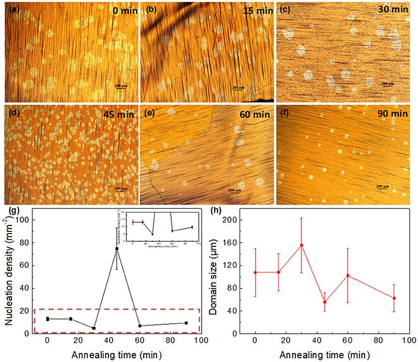
Figure 1. (a–f) Optical images of graphene domains with 30 min growth on Cu foil pretreated with different annealing times in Ar/H2. (a) 0, (b)15, (c) 30, (d) 45, (e) 60, and (f) 90 min. (g,h) Dependence of (g) nucleation density, and (h) graphene domain size on the annealing periods. Inset in g is the enlargement of curves in the red rectangle, showing the error bars in different points.
The surface morphology of Cu foils after annealing for different time periods in a reducing atmosphere was clarified by atomic force microscopy (AFM), as shown in Figure 2. Figure S1 reveals the 3D AFM images, providing a more direct understanding of the topographic evolution of Cu foil substrates. For the pre-oxidized Cu foil without a subsequent annealing period, the substrate exhibited a rather rough surface with the fluctuation as high as 40 nm. (Figure 2a; Figures S1a,b) Annealing in Ar/H2 for 15 min had a smoothing effect on the Cu surface, leaving several big nanoparticles with almost the same fluctuation than that shown in Figure 2a, and smaller nanoparticles at about a quarter of the height (Figure 2b). Further annealing flattened the surface, lowering the size, and height of nanoparticles, as shown in Figure 2c, and Figures S1e,f. The variation trend of nanoparticles on the substrate surface during the annealing process was consistent with that of nucleation density of graphene domains.
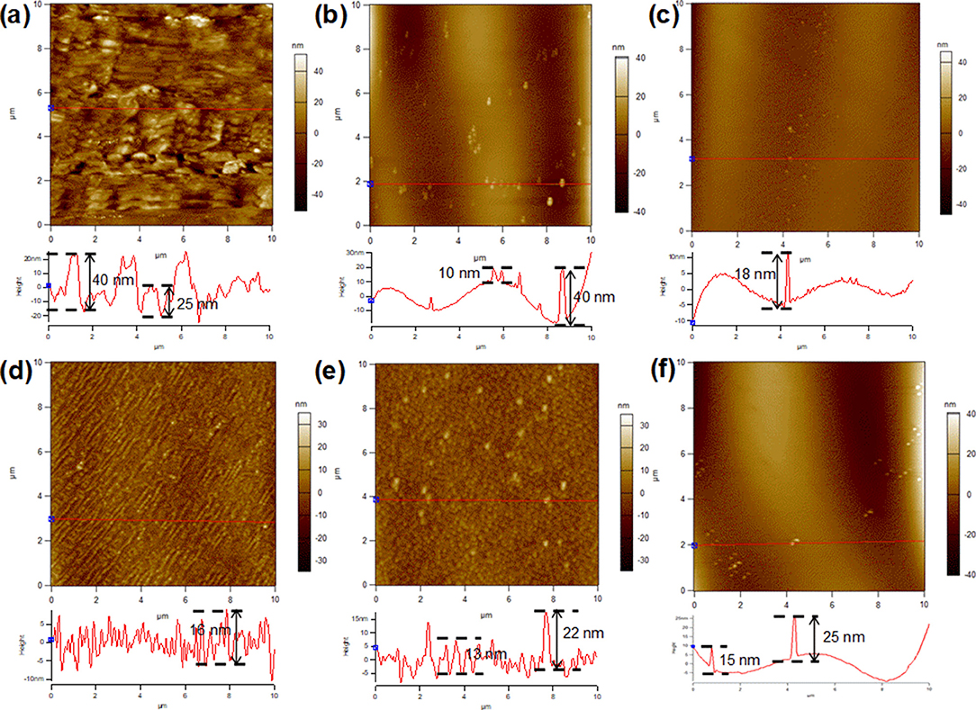
Figure 2. AFM images of Cu foil with an oxide layer pretreated with different annealing times in Ar/H2. (a) 0, (b) 15, (c) 30, (d) 45, (e) 60, and (f) 90 min.
However, extending the annealing time caused a uniformly rough surface with small new nanoparticles, which were considered to come from hydrogen etching, consistent with previous observations (Gan and Luo, 2013) (Figure 2d). In contrast to the evolution of nanoparticles in Figures 2a–c, in this stage, further annealing in Ar/H2 promoted the size growth of nanoparticles, as shown in Figure 2e. In the extended annealing time of 90 and 120 min, with a further reduction of surface oxygen, a competition between the smoothing effect of the high temperature and the etching effect of hydrogen occurred. It is clear that most small nanoparticles vanished because of the smoothing effect, while some nanoparticles grew bigger due to the etching effect (Figure 2f; Figures S2a–c). The difference in the evolution of the nanoparticles may be caused by the uneven distribution of the surface oxygen among them.
The atomic ratio of Cu/O on a copper surface during the annealing process was characterized by XPS, as shown in Figure S3. Based on the results, the effect of surface variation on the nucleation density of graphene domains was further explored. Both the surface defects (such as step edges and nanoparticles) and surface oxidation can lower the energy barrier for the dehydrogenation process of the carbon source. Moreover, the latter possesses greater influence than the former (Hao et al., 2016). It has been speculated that in the initial 30 min annealing process (Figures 2a–c), the degradation of the oxide layer resulted in the formation of nanoparticles with high surface oxygen (Figure S2). The key factor that determines the nucleation density appears to be the density of nanoparticles, since the nanoparticles were both the aggregation points of the surface oxygen and the “defects,” with high fluctuation. However, in the process that followed (Figures 2d–f), the nanoparticles came from hydrogen etching and possessed little surface oxygen. There was no strong correlation between the density of surface nanoparticles and graphene nucleation. In this period, it was difficult to confirm the key factor that determines the nucleation density, since a competition between the points with slight surface oxygen, and the etched nanoparticles with different morphology and height.
Figure 3 reveals the optical images of graphene domains transferred on the SiO2/Si surface. The variation of nucleation density and domain size is in accordance with that in Figure 1. However, the big graphene domains are not single-crystalline, exhibiting near-round shapes with dendritic multilayer graphene branches, as displayed in detail in Figures S2d, S4. Raman measurement was conducted to clarify the structure information of graphene domains. Figure 4b shows the Raman spectra of points marked in Figure 4a. The ratio of the 2D band to the G band (I2D/IG) was calculated as 2.16 and 0.66 for the black point and the red point respectively, indicating single-layer round domains and multilayer graphene branches (Sun et al., 2016). Raman mapping of D, G, and 2D peaks of graphene marked by the rectangle in Figure 4a was also performed, as shown in Figures 4c–e. The relatively high ID in the circle comes from the defects in multilayer structure, while the regions with high ID marked by the black arrows in Figure 4c, were considered to be the result of contaminations on the domain surface. The color contrast in Figure 4f further reveals the layer information in the region, showing the relative uniformity of the single-layer graphene area, and multilayer graphene branches.
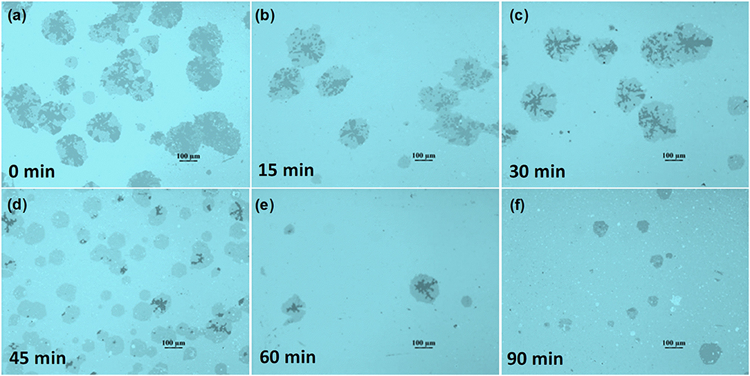
Figure 3. Optical images of graphene domains with 30 min growth after being transferred on the SiO2/Si surface. The corresponding substrate was Cu foil with an oxide layer pretreated with different annealing times in Ar/H2. (a) 0, (b)15, (c) 30, (d) 45, (e) 60, and (f) 90 min.
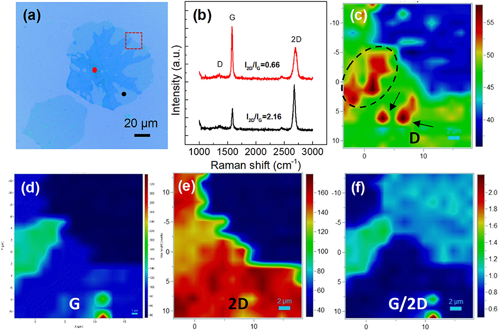
Figure 4. Raman characterization of the obtained graphene domains. (a) Optical image of graphene domains transferred to the SiO2/Si surface. (b) Raman spectra of the black point and the red point marked in a. (c–f) Raman intensity mapping results of (c) D, (d) G, (e) 2D, and (f) G/2D bands of the region marked by red rectangle in (a).
In addition, the crystalline nature of graphene domains was further elucidated by TEM. A domain with a lateral size of about 160 μm was observed after its transfer to a holey carbon supported grid, as shown in Figure 5a. A series of selected area electron diffraction (SAED) patterns were collected. (Figures 5b–h) The layer number was further confirmed by the intensity of the diffraction spots along the line. In region C and D, marked in Figure 5a, the intensity of spots of the outer hexagon is twice or more than that of the inner hexagon, indicating the bilayer (Wu et al., 2017a) or multilayer (Hernandez et al., 2008) stacking of graphene (Figures 5d,e). It was observed that the 6-folded symmetrical SAED patterns of other regions were almost the same, with the intensity ratio of spots in the outer hexagon to the inner hexagon >1, revealing the single-crystal nature of the detected areas (point A,B,E,F,G) (Hernandez et al., 2008). SAED patterns of another domain reveals similar results, as shown in Figure S5. B analyzing the optical images, Raman spectra, and TEM characterization of the obtained graphene domains, it is clear that the structure is composed of a big compact single crystal with near-round shape, and multilayer dendritic structure.
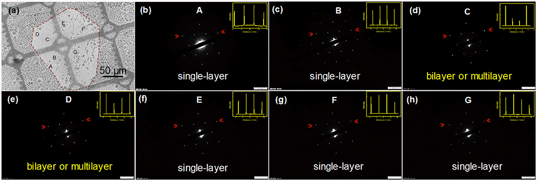
Figure 5. TEM characterization of a graphene domain. (a) SEM image of a graphene domain suspending on a holey carbon supported grid. (b–h) SAED patterns collected from the labeled regions in (a). Inset figures in the upper right are peak intensity profiles from the line marked by two red arrows in the SAED patterns, indicating the stacking style of graphene.
To investigate the formation mechanism of this composite structure, a series of experiments were done, to try eliminate the dendritic graphene branches to obtain pure single crystals. Because hydrogen in the growth duration plays the role of an etching reagent to the graphene edges (Vlassiouk et al., 2011), high H2-to-CH4 ratios were employed by decreasing the proportion of methane for a stronger etching effect with less carbon supply. The optical images of the obtained graphene domains and parameters for preparation are shown in Figure S6, Table S1, respectively. An extremely low domain density was observed with half the flow rate of methane, with only one domain in several fields of view (Figures S6a,e). Graphene domains were difficult to find using optical microscopy after the complicated polymer-assistant transfer process. Moreover, the graphene domains were smaller than 30 μm after growth for 30 min, exhibiting ultralow growth rates compared with other oxygen-assistant methods (Gan and Luo, 2013; Hao et al., 2013; Wu et al., 2017b). Therefore, the growth protocol was not suitable for practical preparation. In addition, reducing the molecular ratio of methane did not seem to decrease the proportion of multilayer graphene branches (Figures S6f,g). The time evolution of graphene domains was also observed, as shown in Figure S7. It is clear that the multilayer graphene branches still exist with a high coverage proportion when the growth time is halved (Figure S7d), revealing that they emerge at the initial stage, rather than being a phenomenon caused by carbon aggregation with the extension of time.
Furthermore, the dendritic graphene branches always attached to the single-crystalline layer and did not exist independently. Together with the above-discussed fact that the growth protocol has little effect on the presence of multilayer graphene branches, it is clear that the surface diffusion of carbon-based species underneath the single crystal plays a vital role in the formation of graphene branches. It has been speculated that in the substrate ramping, and annealing process, the oxide layer on the Cu surface changes the carbon solubility and growth kinetics of graphene (Hao et al., 2016; Sun et al., 2016). The oxide layer possibly also contributed to the accumulation of impurities such as residual metals (Huet and Raskin, 2018). During the growth process, the first single-crystal graphene layer was attributed to the adsorbed carbon atoms on the surface (Gan and Luo, 2013; Hao et al., 2013; Guo et al., 2018), while the multilayer graphene branches formed by active C species passing through the edge of up-layer graphene domains due to the catalytic activity of accumulated residual metal impurities (Zhang et al., 2014; Wu et al., 2017a), or by the diffusion of carbon atoms through the Cu bulk (Hao et al., 2016; Sun et al., 2016). The growth of the single-crystal graphene domains and the multilayer graphene branches was almost synchronous.
The influence of growth temperature on the nucleation density and lateral size of graphene domains was examined, as shown in Figure 6, with the plotted lines shown in Figure S8. The nucleation density decreased from ~4.8 mm−2 to ~2.4 mm−2 with an increasing growth temperature. (Figure S8a), Correspondingly, the size of graphene domains increased with the growth temperature, with the average lateral dimension as large as ~400 μm at 1,070°C (Figure S8b). Moreover, it is obvious that the edge of the domains gradually change from dendritic to compact, as indicated in Figures 6d–f. It has been reported that temperature has a significant influence on the amount and distribution of O species on the surface of the Cu foil (Wang et al., 2016b). At the same time, the proportion of multilayer graphene branches in the domains decreased, possibly due to the modified distribution of residual metal impurities on the surface. With the optimized temperature, extending the growth time to 60 min reveals a large domain size with lateral dimension of ~720 μm (Figure S8c). Further extending the growth time to 120 min lead to the connection of domains, with nearly no space for further lateral dimension growth (Figure S8d).
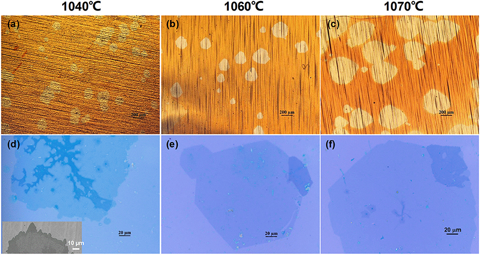
Figure 6. Optical images of the obtained graphene domains prepared with different growth time. (a,d) 1040°C, (b,e) 1060°C, (c,f) 1070°C. Inset in (d) is the SEM image of the dendritic domain edge.
Conclusions
In summary, graphene domains have been synthesized on Cu foil with pre-oxidation, and pre-annealing, composed of a near-round single-crystal layer and dendritic multilayer graphene branches. The dependence of nucleation density and domain size on the Cu surface evolution in the annealing duration in Ar/H2 was clarified. Furthermore, a systematic study in the effect of gas ratio, time, and temperature on graphene domain was undertaken to explore the formation mechanism of the special structures, as impurities such as residual metal impurities accumulated near the Cu surface due to the existence of the oxide layer. The results provide a better understanding of the growth behavior of graphene domains on the Cu surface with an oxide layer originating from the native existence or artificial treatment, paving the way for the synthesis of high-quality graphene films.
Data Availability
The datasets generated for this study are available on request to the corresponding author.
Author Contributions
RZ designed the experiments and wrote the paper. ZZ performed the synthesis of graphene domains. ZX and NL did the characterizations. LH and HZ analyzed the data and modified the article.
Funding
This work was supported by Beijing Natural Science Foundation (2184133).
Conflict of Interest Statement
The authors declare that the research was conducted in the absence of any commercial or financial relationships that could be construed as a potential conflict of interest.
Acknowledgments
Technical help of Yujia Zhong and Xuanliang Zhao are acknowledged.
Supplementary Material
The Supplementary Material for this article can be found online at: https://www.frontiersin.org/articles/10.3389/fmats.2019.00186/full#supplementary-material
References
Cai, W., Moore, A. L., Zhu, Y., Li, X., Chen, S., Shi, L., et al. (2010). Thermal transport in suspended and supported monolayer graphene grown by chemical vapor deposition. Nano Lett. 10, 1645–1651. doi: 10.1021/nl9041966
Chen, J., Cui, M., Wu, G., Wang, T., Mbengue, J. M., Li, Y., et al. (2017). Fast growth of large single-crystalline graphene assisted by sequential double oxygen passivation. Carbon 116, 133–138. doi: 10.1016/j.carbon.2017.01.108
Ding, D., Solís-Fernández, P., Yunus, R. M., Hibino, H., and Ago, H. (2017). Behavior and role of superficial oxygen in Cu for the growth of large single-crystalline graphene. Appl. Surf. Sci. 408, 142–149. doi: 10.1016/j.apsusc.2017.02.250
Gan, L., and Luo, Z. (2013). Turning off hydrogen to realize seeded growth of subcentimeter single-crystal graphene grains on copper. ACS Nano 7, 9480–9488. doi: 10.1021/nn404393b
Grantab, R., Shenoy, V. B., and Ruoff, R. S. (2010). Anomalous strength characteristics of tilt grain boundaries in graphene. Science 330, 946–948. doi: 10.1126/science.1196893
Guo, W., Jing, F., Xiao, J., Zhou, C., Lin, Y., and Wang, S. (2016). Oxidative-etching-assisted synthesis of centimeter-sized single-crystalline graphene. Adv. Mater. 28, 3152–3158. doi: 10.1002/adma.201503705
Guo, W., Wu, B., Wang, S., and Liu, Y. (2018). Controlling fundamental fluctuations for reproducible growth of large single-crystal graphene. ACS Nano 12, 1778–1784. doi: 10.1021/acsnano.7b08548
Han, G. H., Güneş, F., Bae, J. J., Kim, E. S., Chae, S. J., Shin, H., et al. (2011). Influence of copper morphology in forming nucleation seeds for graphene growth. Nano Lett. 11, 4144–4148. doi: 10.1021/nl201980p
Hao, Y., Bharathi, M. S., Wang, L., Liu, Y., Chen, H., Nie, S., et al. (2013). The role of surface oxygen in the growth of large single-crystal graphene on copper. Science 342, 720–723. doi: 10.1126/science.1243879
Hao, Y., Wang, L., Liu, Y., Chen, H., Wang, X., Tan, C., et al. (2016). Oxygen-activated growth and bandgap tunability of large single-crystal bilayer graphene. Nat. Nanotechnol. 11, 426–431. doi: 10.1038/nnano.2015.322
Hernandez, Y., Nicolosi, V., Lotya, M., Blighe, F. M., Sun, Z., De, S., et al. (2008). High-yield production of graphene by liquid-phase exfoliation of graphite. Nat. Nanotechnol. 3, 563–568. doi: 10.1038/nnano.2008.215
Huet, B., and Raskin, J. (2018). Role of Cu foil in-situ annealing in controlling the size and thickness of CVD graphene domains. Carbon 129, 270–280. doi: 10.1016/j.carbon.2017.12.043
Jo, I., Park, S., Kim, D., Moon, J. S., Park, W. B., Kim, T. H., et al. (2018). Tension-controlled single-crystallization of copper foils for roll-to-roll synthesis of high-quality graphene films. 2D Mater. 5:24002. doi: 10.1088/2053-1583/aaa7b8
Kim, S. M., Hsu, A., Lee, Y. H., Dresselhaus, M., Palacios, T., Kim, K. K., et al. (2013). The effect of copper pre-cleaning on graphene synthesis. Nanotechnology 24:365602. doi: 10.1088/0957-4484/24/36/365602
Lee, J. H., Lee, E. K., Joo, W. J., Jang, Y., Kim, B. S., Lim, J. Y., et al. (2014). Wafer-scale growth of single-crystal monolayer graphene on reusable hydrogen-terminated germanium. Science 344, 286–289. doi: 10.1126/science.1252268
Li, J., Wang, X., Liu, X., Jin, Z., Wang, D., and Wan, L. (2015). Facile growth of centimeter-sized single-crystal graphene on copper foil at atmospheric pressure. J. Mater. Chem. C. 3, 3530–3535. doi: 10.1039/C5TC00235D
Li, X., Colombo, L., and Ruoff, R. S. (2016). Synthesis of graphene films on copper foils by chemical vapor deposition. Adv. Mater. 28, 6247–6252. doi: 10.1002/adma.201504760
Li, X., Magnuson, C. W., Venugopal, A., Tromp, R. M., Hannon, J. B., Vogel, E. M., et al. (2011). Large-area graphene single crystals grown by low-pressure chemical vapor deposition of methane on copper. J. Am. Chem. Soc. 133, 2816–2819. doi: 10.1021/ja109793s
Lin, L., Sun, L., Zhang, J., Sun, J., Koh, A. L., Peng, H., et al. (2016). Rapid growth of large single-crystalline graphene via second passivation and multistage carbon supply. Adv. Mater. 28, 4671–4677. doi: 10.1002/adma.201600403
Mohsin, A., Liu, L., Liu, P., Deng, W., Ivanov, I. N., Li, G., et al. (2013). Synthesis of millimeter-size hexagon-shaped graphene single crystals on resolidified copper. ACS Nano 7, 8924–8931. doi: 10.1021/nn4034019
Nguyen, V. L., Shin, B. G., Duong, D. L., Kim, S. T., Perello, D., Lim, Y. J., et al. (2015). Seamless stitching of graphene domains on polished copper (111) foil. Adv. Mater. 27, 1376–1382. doi: 10.1002/adma.201404541
Shi, Y. G., Wang, D., Zhang, J. C., Zhang, P., Shi, X. F., and Hao, Y. (2014). Fabrication of single-crystal few-layer graphene domains on copper by modified low-pressure chemical vapor deposition. Crystengcomm 16, 7558–7563. doi: 10.1039/C4CE00744A
Song, Y., Pan, D., Cheng, Y., Wang, P., Zhao, P., and Wang, H. (2015). Growth of large graphene single crystal inside a restricted chamber by chemical vapor deposition. Carbon 95, 1027–1032. doi: 10.1016/j.carbon.2015.08.115
Sun, H., Han, Y., Wu, J., Lu, Y., Xu, J., Luo, Y., et al. (2016). Cooling growth of millimeter-size single-crystal bilayer graphene at atmospheric pressure. J. Phys. Chem. C 120, 13596–13603. doi: 10.1021/acs.jpcc.6b04105
Tsen, A. W., Brown, L., Levendorf, M. P., Ghahari, F., Huang, P. Y., Havener, R. W., et al. (2012). Tailoring electrical transport across grain boundaries in polycrystalline graphene. Science 6085, 1143–1146. doi: 10.1126/science.1218948
Vlassiouk, I., Regmi, M., Fulvio, P., Dai, S., Datskos, P., Eres, G., et al. (2011). Role of hydrogen in chemical vapor deposition growth of large single-crystal graphene. ACS Nano 5, 6069–6076. doi: 10.1021/nn201978y
Wang, H., Wang, G., Bao, P., Yang, S., Zhu, W., Xie, X., et al. (2012). Controllable synthesis of submillimeter single-crystal monolayer graphene domains on copper foils by suppressing nucleation. J. Am. Chem. Soc. 134, 3627–3630. doi: 10.1021/ja2105976
Wang, H., Xu, X., Li, J., Lin, L., Sun, L., Sun, X., et al. (2016a). Surface monocrystallization of copper foil for fast growth of large single-crystal graphene under free molecular flow. Adv. Mater. 28, 8968–8974. doi: 10.1002/adma.201603579
Wang, S., Hibino, H., Suzuki, S., and Yamamoto, H. (2016b). Atmospheric pressure chemical vapor deposition growth of millimeter-scale single-crystalline graphene on the copper surface with a native oxide layer. Chem. Mater. 28, 4893–4900. doi: 10.1021/acs.chemmater.6b00252
Wang, Y., Cheng, Y., Wang, Y., Zhang, S., Zhang, X., Yin, S., et al. (2018). Oxide-assisted growth of scalable single-crystalline graphene with seamlessly stitched millimeter-sized domains on commercial copper foils. RSC Adv. 8, 8800–8804. doi: 10.1039/C8RA00770E
Wu, J., Wang, J., Pan, D., Li, Y., Jiang, C., Li, Y., et al. (2017a). Synchronous growth of high-quality bilayer bernal graphene: from hexagonal single-crystal domains to wafer-scale homogeneous films. Adv. Funct. Mater. 27:1605927. doi: 10.1002/adfm.201605927
Wu, R., Pan, J., Ou, X., Zhang, Q., Ding, Y., Sheng, P., et al. (2017b). Concurrent fast growth of sub-centimeter single-crystal graphene with controlled nucleation density in a confined channel. Nanoscale 9, 9631–9640. doi: 10.1039/C7NR02741A
Xu, X., Zhang, Z., Dong, J., Yi, D., Niu, J., Wu, M., et al. (2017). Ultrafast epitaxial growth of metre-sized single-crystal graphene on industrial Cu foil. Sci. Bull. 62, 1074–1080. doi: 10.1016/j.scib.2017.07.005
Xu, X., Zhang, Z., Qiu, L., Zhuang, J., Zhang, L., Wang, H., et al. (2016). Ultrafast growth of single-crystal graphene assisted by a continuous oxygen supply. Nat. Nanotechnol. 11, 930–935. doi: 10.1038/nnano.2016.132
Yan, Z., Lin, J., Peng, Z., Sun, Z., Zhu, Y., Li, L., et al. (2012). Toward the synthesis of wafer-scale single-crystal graphene on copper foils. ACS Nano 6, 9110–9117. doi: 10.1021/nn303352k
Keywords: graphene domains, controllable nucleation, oxide layer, surface morphology, chemical vapor deposition
Citation: Zhang R, He L, Zhen Z, Xu Z, Li N and Zhu H (2019) Controlled Nucleation of Graphene Domains on Copper With an Oxide Layer by Atmospheric Pressure Chemical Vapor Deposition. Front. Mater. 6:186. doi: 10.3389/fmats.2019.00186
Received: 21 May 2019; Accepted: 18 July 2019;
Published: 02 August 2019.
Edited by:
Xu Zhang, Argonne National Laboratory (DOE), United StatesReviewed by:
Qingqing Ji, Massachusetts Institute of Technology, United StatesKarthik Ramasamy, Los Alamos National Laboratory (DOE), United States
Copyright © 2019 Zhang, He, Zhen, Xu, Li and Zhu. This is an open-access article distributed under the terms of the Creative Commons Attribution License (CC BY). The use, distribution or reproduction in other forums is permitted, provided the original author(s) and the copyright owner(s) are credited and that the original publication in this journal is cited, in accordance with accepted academic practice. No use, distribution or reproduction is permitted which does not comply with these terms.
*Correspondence: Limin He, aGVfbGltaW5Ac29odS5jb20=; Hongwei Zhu, aG9uZ3dlaXpodUB0c2luZ2h1YS5lZHUuY24=