 Yee Sin Ang1,2*
 L. K. Ang1,2*
- 1Science and Math, Singapore University of Technology and Design, Singapore, Singapore
- 2Engineering Product Development, Singapore University of Technology and Design, Singapore, Singapore
Understanding the physics of charge transport in organic materials and charge injection across organic-based interface is critically important for the development of novel organic electronics and optoelectronics. Despite extensive efforts devoted to the study of transport and injection phenomena in organic materials and interfaces, the physics of thermionic carrier injection across graphene/organic interface remains largely incomplete thus far. Here we construct a model of thermionic carrier injection across a graphene/organic Schottky interface based on the Lengevin theory of charge recombination and the detailed balance formalism. We show that, due to the strong electrostatic doping effect in graphene under the influence of an external gate voltage, the electrical current traversing the interface differs significantly from conventional bulk-metal/organic Schottky interface and the injection current can be efficiently modulated by a gate-voltage to achieve an on-off ratio well-exceed 107. The model developed here shall provide a theoretical foundation for the understanding graphene/organic Schottky interface, thus paving the way toward the development of novel nanoscale graphene-hybrid organic electronic and optoelectronic devices.
1. Introduction
Thermionic charge injection across an interface formed between a metal and a crystalline semiconductor is governed by the celebrated Richardson-Schottky (RS) equation:
where J is the electrical current density, m* is the electron effective mass in the metal, and w is the depletion width in the semiconductor. For solids with low carrier mobility, such as amorphous solid and organic semiconductors, Equation (1) is no longer valid as demonstrated in the pioneering works of Simmons (Simmons, 1965), Emtage and O'Dwyer (Emtage and O'Dwyer, 1966), and Crowell and Sze in 1960s' (Crowell and Sze, 1966). As illustrated in a more recent work by Scott and Malliaras (SM) (Scott and Malliaras, 1999; Scott, 2003) based on the detailed balance and the Langevin theory of charge recombination, the thermionic charge injection across a metal/organic interface is governed by an analytical non-Richardson-Dushman relation,
where ψ is a voltage-dependent term related to the image charge effect. In contrast to the RD model, the metal material parameters is completely absent in the pre-exponential factor in Equation (2) and the tunneling current is directly proportional to μ and N0, the mobility and the density of transport sites in the organic materials, respectively. Such unconventional μ-dependence, absent in the classic RS model, has been experimentally confirmed (Shen et al., 2001). Importantly, the SM model provides a useful analytical tool for the analysis of thermionic charge injection in bulk-metal/organic Schottky interface where the classic RS equation in Equation (1) breaks down.
Recently, integrating low-dimensional carbon-based nanomaterials, such as two-dimensional (2D) graphene and one-dimensional (1D) carbon nanotube (Sarker and Khondaker, 2012), with organic materials for electronic applications has become one of the active research topics (Kim and Kymissis, 2017; Gobbi et al., 2018). Particularly for graphene, recent experimental works has demonstrated graphene being integrated into the design of organic electronics as electrode (Di et al., 2008), transistor (Hlaing et al., 2015; Kim et al., 2015, 2016), photodiode (Kim et al., 2017), sensor (Choi et al., 2015), light-emitting diode (Ricciardulli et al., 2018), and so on. Despite numerous ongoing efforts to uncover the unusual transport physics (Ang and Ang, 2016; Ang et al., 2017a,b, 2018; Trushin, 2018; Pasadas et al., 2019) and device application potential (Yang et al., 2012; Ojeda-Aristizabal et al., 2013; Sinha and Lee, 2014) of graphene-based devices, a comprehensive physical model that underlies the thermionic charge injection mechanism across a hybrid graphene/organic Schottky interface remains incomplete thus far. It should be noted that, due to the atomic-thickness and the linear energy dispersion of graphene (Castro Neto et al., 2009), the Fermi level in graphene can be sensitively tuned by several strategies, such as electrostatic doping via an external gate voltage (Yu et al., 2009), chemical doping (Liu et al., 2011), and light doping (Fang et al., 2012). In relevance to Schottky interface, the electrostatically tunable graphene Fermi level manifests as a gate-tunable Schottky barrier height which allows the thermionic injection current to be exponentially modulated, thus offering exceptional electrical switching capability as a barrister device (Yang et al., 2012).
Despite the increasing research spotlight received by graphene/organinc hybrid devices in recent years, a dedicated transport model for the charge injection phenomena across a graphene/organic Schottky interface remains lacking. In this work, we expand the SM model to the case of graphene/organic Schottky contact (see Figure 1A) where the Fermi level shifting due to gate and bias voltages is explicitly taken into account. Due to the strong electrostatic doping effect in graphene, the bias-voltage-dependence of the injection current density is significantly modified. Using a top-gated graphene/organic Schottky diode as a proof of concept device, we show that the thermionic injection current can be efficiently controlled by a gate voltage, exhibiting an exceptionally large current on/off ratio of >107. The theoretical model developed here shall lay a useful theoretical foundation for the analysis, modeling, and design of graphene/organic electronic and optoelectronic devices.
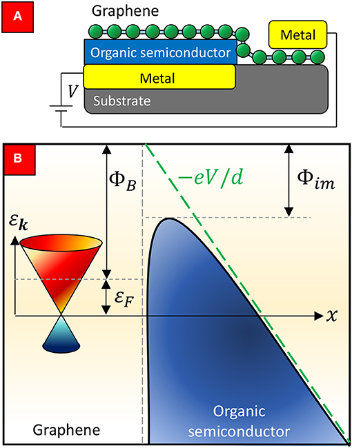
Figure 1. Concept of thermionic carrier injection in graphene/organic Schottky interface. (A) Schematic drawing of a graphene/organic Schottky contact; (B) Energy band diagram of graphene/organic interface, where represents the image charge effect.
2. Theory
The charge injection from metal into a low mobility material, such as insulator and organic material, was extensively studied by Emtage and O'Dwyer based on a drift-diffusion model Emtage and O'Dwyer (1966). Here we adopt an equivalent analytical theory of thermionic-based carrier injection in the contact-limited transport regime developed by Scott and Malliaras (1999) based on the detailed balance principle and the carrier recombination near the metal/organic interface as described by the Langevin theory. At the vicinity of the graphene/organic interface as shown in Figure 1B, the electrostatic potential energy profile is given as
where ΦB is the Schottky barrier height of the metal/semiconductor interface, V is the applied bias voltage, d is the thickness of the organic semiconductor, ε is the dielectric constant of the organic semiconductor, ε0 is the permittivity of free space, and the final term represents the image potential effect. Here we have ignored the space-charge field, which is well-justified when the charge transport is highly contact-limited (Scott, 2003). A charged carrier attempting to “fly-over” the potential peak on the semiconductor side can recombine with its image charge induced on the metal surface when the Coulombic binding energy between the carrier-image pair exceeds the thermal energy kBT. By equating the thermal energy, kBT with the Coulombic binding energy , the characteristic Coulomb radius can be expressed as . We first consider the case of zero-bias, i.e., V = 0. In this case, the image potential term exceeds kBT when the distance from the metal/organic interface is smaller than xc, and can be solved from Φ(xc, 0) − ΦB = kBT to yield xc = rc/4. Charged carries residing within xc from the interface eventually recombine since the Coulombic energy exceeds the thermal energy. The zero-bias recombination current density at x = xc can thus be written as
where n0 is the surface carrier density at xc, μ is the electrical mobility of the organic material and the local electric field strength at xc is
The recombination current density can thus be written as , where the negative sign signifies that the current is flowing in the −x direction, i.e., from the organic material into graphene. The detailed balance condition then requires
where Jth, 0 is the zero-voltage thermionic injection current density, which can be assumed to take the Arrhenius form of Jc ≈ exp(−ΦB/kBT). For the detailed balance condition to hold for all temperature, the n0 in Jr must contain the same exponential dependence (Scott and Malliaras, 1999), i.e., n0 = N0 exp (ΦB/kBT), and N0 is the density of transport sites. Hence, we arrived at the MG zero-bias thermionic injection current density of
A hallmark of Equation (7) is the absence of material parameters of the metal in the effective Richardson constant, and the presence of μ-dependence as verified experimentally (Shen et al., 2001).
Up till Equation (7), the recombination and the injection current densities are identical for both conventional bulk-metal/organic and graphene/organic interface in the zero-bias limit. The distinction becomes more dramatic with finite-bias, V ≠ 0, where the field-effect tunning of graphene Fermi level can sensitively influence the charge injection. For graphene, the energy dispersion is described by linear Dirac equation, εk = ℏvF |k|, where m/s is the Fermi velocity and k is the 2D crystal momentum lying in the 2D plane of graphene. The density of states (DOS) is linear in εk, i.e., where gsv = 4 is the spin-valley degeneracy. The carrier density in graphene, i.e., , can be obtained as
Correspondingly, the Fermi level becomes
where sign(x) is the sign function. In the presence of a bias-voltage, additional charge carriers are induced on graphene. Consider a planar diode geometry as shown in Figure 1, the parallel-plate capacitor model can be used to calculate the induced carrier density,
and the negative sign is necessitate since when a positive (negative) bias is applied, positively (negatively) charged holes (electrons) are induced on the graphene sheet for the device shown in Figure 1B. The total carrier density on graphene sheet is then given by
and this results in a shifting of the Fermi level. From Equation (9), the shifted Fermi level can then be calculated as
where and ξ ≡ sign(εF0). Correspondingly, the Schottky barrier height becomes bias-dependent, i.e.,
and
From Equation (3), the ΦB(x, V) peaks at
which corresponds to a peak potential of
where the square-root term represents the usual Schottky barrier-lowering effect while the ΔΦB(V) represents the field-effect tunning of the Schottky barrier height which arises due to the reduced-dimensionality and the linear energy dispersion of graphene. We now determine the voltage-dependent critical distance, xc, V, below which charge-image recombination occurs. The xc(V) corresponds to the position where Φmax − Φ(xc, V, V) = kBT, which yields the xc, V-quadratic relation:
After some algebra, we obtain xc, V as
where we have chosen the solution that is closest to the interface, and f ≡ rceV/kBTd. The bias-dependent recombination current can then be expressed as
where . Similarly, the thermionic injection current density is expected to take the form,
where the first exponential term corresponds to the gate-tunability of Φmax as shown in Equation (16) and the second exponential term corresponds to the usual Schottky effect. Knowing that the net injection current density is given by the relation J(V) = Jth,V − Jr,V = n0,VeV where n0,V is the bias-dependent surface carrier density at xc,V, we obtain
and the net thermionic injection current at V > 0 becomes
Here the material properties of graphene is coupled to the transport current density through ΔΦB(V), which is in stark contrast to the case of conventional metal/inorganic interface where the transport current is independent of metal properties. Interestingly, the square-root term in the square parenthesis which corresponds to the electrostatic doping of graphene can be rewritten in terms of a characteristic Coulomb energy parameter as , where we have defined the characteristic Coulomb energy parameter,
At room temperature and consider a typical dielectric constant of ε = 3.5 and graphene Fermi velocity m/s, the Coulomb energy parameter at room temperature is εC ≈ 10.4 meV. By combining Equations (22) and (23), we obtain
which can be compactly written as
where J0(T) ≡ (4N0μkBT/rC) exp (−ΦB/kBT). Importantly, it can be seen from Equation (24) that the injection current is directly proportional to the density of the transport sites in the organic semiconductor, N0, which can be controlled by appropriately doping the organic semiconductor (Shen et al., 2003). Such feature is absence in the classic thermionic emission model in Equation (1), and thus shall provide a distinctive smoking signature for experimental verification.
3. Results and Discussions
Equation (25) represents the central result of this work. The physical significance can be clearly seen. In addition to the conventional Schottky image potential effect as encoded in the term exp(f1/2), the thermionic injection current is further enhanced by the electrostatic doping effect in graphene in the presence of an bias voltage. This significantly modifies the current voltage-characteristics as shown in Figure 2 where we have used ε = 3.5 and T = 300 K. At low applied bias voltage, both SM model and the graphene/organic model developed are in good mutual agreement. However, at large applied bias voltage when the electrostatic doping effect in graphene becomes sufficiently strong, the field-induced enhancement of the thermionic injection current in graphene/organic Schottky interface becomes obvious as compared to the SM model where such electrostatic doping effect negligible due to the strong screening of external electric field in conventional bulk metal. Such field-enhanced thermionic injection is especially obvious around the Dirac point, i.e., εF0 ≈ 0 due to vanishing carrier density which strongly amplifies the field-induced Fermi level shifting. For εF0 = −0.05 eV, the thermionic injection current increases sharply when εF is scanned across the Dirac point (see Figure 2), and this results in over two-order of magnitudes enhancement of the injection current compared to that of the SM model.
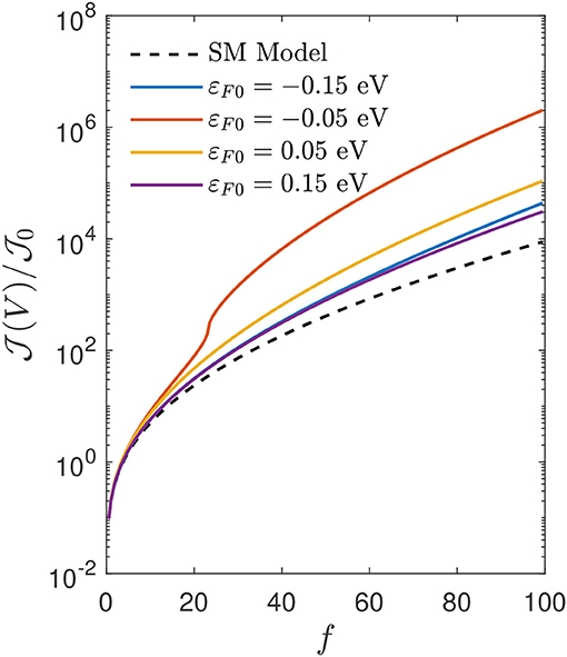
Figure 2. Current-voltage characteristics of thermionic carrier injection in graphene/organic Schottky contact at various intrinsic Fermi level, εF0, with organic semiconductor dielectric constant ε = 3.5 and room temperature T = 300 K.
In Figure 3, we show the transfer characteristic of a field-effect Schottky barrier transistor device based on a top-gated graphene/organic Schottky contact. The schematic drawing of the device is shown in the inset of Figure 3. The top gate introduces an additional term in Equation (25), i.e.,
where , , , dG is the thickness of the gate insulator, εG is the dielectric constant of the gate insulator, and . The transfer characteristic curve is calculated by considering a dG = 5 nm thin Al2O3 of εG = 6.4 as the gate dielectric, which is typically used in graphene field-effect devices (Kim et al., 2009; Pedrinazzi et al., 2017). A rapidly raising injection current density is clearly visible at gate voltages slightly larger than 0, which corresponds to the much enhanced field effect when the Fermi level crosses the Dirac point as discussed above in Figure 2. It can be seen from Figure 3 that the current can be switched over several orders of magnitude when VG is tuned from −2 to +2 V, thus yielding an exceptionally large current on-off ratio of >107 at room temperature. This predicted large on-off ratio is also consistent with the experimental values ranging from 103 to 106 in graphene-based organic barristor (Lemaitre et al., 2012; Hlaing et al., 2015; Oh et al., 2015; Kim et al., 2016).
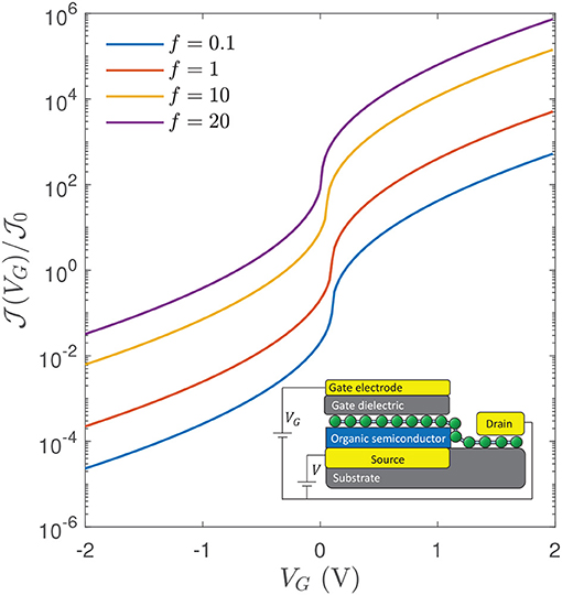
Figure 3. Transfer characteristics of a top-gated graphene/organic field-effect Schottky barrier transistor at various bias voltage parameter, f. Inset shows the schematic drawing of the device. The injection current is calculated by considering a gate dielectric thickness of dG = 5 nm and of dielectric constant εG = 6.4 which is typical for Al2O3 gate dielectric. The organic semiconductor dielectric constant is assumed to be ε = 3.5 and the device is operated at room temperature T = 300 K.
Finally, we remark that the we have considered a field-independent carrier mobility, μ, in modeling the injection currents in Figures 2, 3. In general, the carrier mobility can have complex dependencies on the applied electric field strength (Blom et al., 1997), carrier density (Pasveer et al., 2005), and spatial disorders (Zubair et al., 2018), and such effect can be readily incorporated in the graphene/organic thermionic injection model developed above. Especially for organic semiconductor with field-dependent mobility, such as poly(dialkoxy p-phenylene vinylene), the current-voltage characteristic is expected to be appreciably altered. The field-dependent mobility takes the form of (Pai, 1970; Blom et al., 1997),
where μ(0) is the zero-field mobility, and γ is a material-dependent constant. In this case, the mobility term in the injection current density should be replaced by μ[E(xc, V)], where the electric field strength at the injection position xc is
By combining Equations (26) and (27) evaluated at Ec, V, we obtain the current-voltage characteristics for a Schottky interface composed of graphene and an organic semiconductor with field-dependent mobility as
where .
It should be further noted that the Schottky contact model developed above falls in the contact-limited transport regime where the electrical characteristics is dominated by the interfacial charge injection (Simmons, 1965), while is minimally influenced by the bulk effects, such as the field-effect tuning of the carrier density in the organic semiconductor and the space-charge-limited transport (Zhang et al., 2017). Such bulk effects shall become important for the drift-diffusion modeling of carriers in the bulk-limited transport regime.
4. Conclusion
In summary, an analytical model of thermionic carrier injection in graphene/organic Schottky interface is developed in this work. It is shown that due to the presence of strong electrostatic doping effect in graphene in which the Fermi level is sensitively shifted by an applied bias voltage, the current-voltage characteristics in graphene/organic Schottky contact can differ significantly from conventional bulk-metal/organic Schottky contact, especially in the high bias regime. We further show that a top-gated graphene/organic Schottky contact can be used as a transistor device with exceptionally large on-off ratio >107, which is consistent with the large current on-off ratio previously observed in the experiments. These findings shall provide a theoretical foundation useful for the analysis, modeling, and design of graphene/organic hybrid electronic and optoelectronic devices.
Data Availability
The datasets generated for this study are available on request to the corresponding author.
Author Contributions
All authors listed have made a substantial, direct and intellectual contribution to the work, and approved it for publication.
Funding
This work is supported by A*STAR-IRG (A1783c0011) and AFOSR AOARD (FA2386-17-1-4020).
Conflict of Interest Statement
The authors declare that the research was conducted in the absence of any commercial or financial relationships that could be construed as a potential conflict of interest.
References
Ang, Y., Liang, S.-J., and Ang, L. (2017a). Theoretical modeling of electron emission from graphene. MRS Bull. 42, 505–510. doi: 10.1557/mrs.2017.141
Ang, Y. S., and Ang, L. K. (2016). Current-temperature scaling for a schottky interface with nonparabolic energy dispersion. Phys. Rev. Appl. 6:034013. doi: 10.1103/PhysRevApplied.6.034013
Ang, Y. S., Yang, H. Y., and Ang, L. K. (2018). Universal scaling laws in schottky heterostructures based on two-dimensional materials. Phys. Rev. Lett. 121:056802. doi: 10.1103/PhysRevLett.121.056802
Ang, Y. S., Zubair, M., and Ang, L. K. (2017b). Relativistic space-charge-limited current for massive dirac fermions. Phys. Rev. B 95:165409. doi: 10.1103/PhysRevB.95.165409
Blom, P. W. M., de Jong, M. J. M., and van Munster, M. G. (1997). Electric-field and temperature dependence of the hole mobility in poly(p-phenylene vinylene). Phys. Rev. B 55, R656–R659. doi: 10.1103/PhysRevB.55.R656
Castro Neto, A. H., Guinea, F., Peres, N. M. R., Novoselov, K. S., and Geim, A. K. (2009). The electronic properties of graphene. Rev. Mod. Phys. 81, 109–162. doi: 10.1103/RevModPhys.81.109
Choi, K., Nam, S., Lee, Y., Lee, M., Jang, J., Kim, S. J., et al. (2015). Reduced water vapor transmission rate of graphene gas barrier films for flexible organic field-effect transistors. ACS Nano 9, 5818–5824. doi: 10.1021/acsnano.5b01161
Crowell, C., and Sze, S. (1966). Current transport in metal-semiconductor barriers. Solid State Electron. 9, 1035–1048. doi: 10.1016/0038-1101(66)90127-4
Di, C.-A., Wei, D., Yu, G., Liu, Y., Guo, Y., and Zhu, D. (2008). Patterned graphene as source/drain electrodes for bottom-contact organic field-effect transistors. Adv. Mater. 20, 3289–3293. doi: 10.1002/adma.200800150
Emtage, P. R., and O'Dwyer, J. J. (1966). Richardson-schottky effect in insulators. Phys. Rev. Lett. 16, 356–358. doi: 10.1103/PhysRevLett.16.356
Fang, Z., Wang, Y., Liu, Z., Schlather, A., Ajayan, P. M., Koppens, F. H., et al. (2012). Plasmon-induced doping of graphene. ACS Nano 6, 10222–10228. doi: 10.1021/nn304028b
Gobbi, M., Orgiu, E., and Samorì, P. (2018). When 2d materials meet molecules: opportunities and challenges of hybrid organic/inorganic van der waals heterostructures. Adv. Mater. 30:1706103. doi: 10.1002/adma.201706103
Hlaing, H., Kim, C.-H., Carta, F., Nam, C.-Y., Barton, R. A., Petrone, N., et al. (2015). Low-voltage organic electronics based on a gate-tunable injection barrier in vertical graphene-organic semiconductor heterostructures. Nano Lett. 15, 69–74. doi: 10.1021/nl5029599
Kim, B. J., Hwang, E., Kang, M. S., and Cho, J. H. (2015). Electrolyte-gated graphene schottky barrier transistors. Adv. Mater. 27, 5875–5881. doi: 10.1002/adma.201502020
Kim, C.-H., and Kymissis, I. (2017). Graphene–organic hybrid electronics. J. Mater. Chem. C 5, 4598–4613. doi: 10.1039/C7TC00664K
Kim, J. S., Choi, Y. J., Woo, H. J., Yang, J., Song, Y. J., Kang, M. S., et al. (2017). Schottky-barrier-controllable graphene electrode to boost rectification in organic vertical p–n junction photodiodes. Adv. Funct. Mater. 27:1704475. doi: 10.1002/adfm.201704475
Kim, J. S., Kim, B. J., Choi, Y. J., Lee, M. H., Kang, M. S., and Cho, J. H. (2016). An organic vertical field-effect transistor with underside-doped graphene electrodes. Adv. Mater. 28, 4803–4810. doi: 10.1002/adma.201505378
Kim, S., Nah, J., Jo, I., Shahrjerdi, D., Colombo, L., Yao, Z., et al. (2009). Realization of a high mobility dual-gated graphene field-effect transistor with al2o3 dielectric. Appl. Phys. Lett. 94:062107. doi: 10.1063/1.3077021
Lemaitre, M. G., Donoghue, E. P., McCarthy, M. A., Liu, B., Tongay, S., Gila, B., et al. (2012). Improved transfer of graphene for gated schottky-junction, vertical, organic, field-effect transistors. ACS Nano 6, 9095–9102. doi: 10.1021/nn303848k
Liu, H., Liu, Y., and Zhu, D. (2011). Chemical doping of graphene. J. Mater. Chem. 21, 3335–3345. doi: 10.1039/C0JM02922J
Oh, G., Kim, J.-S., Jeon, J. H., Won, E., Son, J. W., Lee, D. H., et al. (2015). Graphene/pentacene barristor with ion-gel gate dielectric: flexible ambipolar transistor with high mobility and on/off ratio. ACS Nano 9, 7515–7522. doi: 10.1021/acsnano.5b02616
Ojeda-Aristizabal, C., Bao, W., and Fuhrer, M. S. (2013). Thin-film barristor: a gate-tunable vertical graphene-pentacene device. Phys. Rev. B 88:035435. doi: 10.1103/PhysRevB.88.035435
Pai, D. M. (1970). Transient photoconductivity in poly(n-vinylcarbazole). J. Chem. Phys. 52, 2285–2291. doi: 10.1063/1.1673300
Pasadas, F., Saeed, M., Hamed, A., Wang, Z., Negra, R., Neumaier, D., et al. (2019). Large-signal model of the metal-insulator-graphene diode targeting rf applications. IEEE Electron Device Lett. 40, 1005–1008. doi: 10.1109/LED.2019.2911116
Pasveer, W. F., Cottaar, J., Tanase, C., Coehoorn, R., Bobbert, P. A., Blom, P. W., et al. (2005). Unified description of charge-carrier mobilities in disordered semiconducting polymers. Phys. Rev. Lett. 94:206601. doi: 10.1103/PhysRevLett.94.206601
Pedrinazzi, P., Mansouri, A., Habibpour, O., Winters, M., Rorsman, N., Behnam, A., et al. (2017). High-gain graphene transistors with a thin alox top-gate oxide. Sci. Rep. 7:2419. doi: 10.1038/s41598-017-02541-2
Ricciardulli, A. G., Yang, S., Wetzelaer, G.-J. A. H., Feng, X., and Blom, P. W. M. (2018). Hybrid silver nanowire and graphene-based solution-processed transparent electrode for organic optoelectronics. Adv. Funct. Mater. 28:1706010. doi: 10.1002/adfm.201706010
Sarker, B. K., and Khondaker, S. I. (2012). Thermionic emission and tunneling at carbon nanotube–organic semiconductor interface. ACS Nano 6, 4993–4999. doi: 10.1021/nn300544v
Scott, J., and Malliaras, G. G. (1999). Charge injection and recombination at the metal–organic interface. Chem. Phys. Lett. 299, 115–119. doi: 10.1016/S0009-2614(98)01277-9
Scott, J. C. (2003). Metal–organic interface and charge injection in organic electronic devices. J. Vacuum Sci. Technol. A 21, 521–531. doi: 10.1116/1.1559919
Shen, Y., Diest, K., Wong, M. H., Hsieh, B. R., Dunlap, D. H., and Malliaras, G. G. (2003). Charge transport in doped organic semiconductors. Phys. Rev. B 68:081204. doi: 10.1103/PhysRevB.68.081204
Shen, Y., Klein, M. W., Jacobs, D. B., Campbell Scott, J., and Malliaras, G. G. (2001). Mobility-dependent charge injection into an organic semiconductor. Phys. Rev. Lett. 86, 3867–3870. doi: 10.1103/PhysRevLett.86.3867
Simmons, J. G. (1965). Richardson-Schottky effect in solids. Phys. Rev. Lett. 15, 967–968. doi: 10.1103/PhysRevLett.15.967
Sinha, D., and Lee, J. U. (2014). Ideal graphene/silicon schottky junction diodes. Nano Lett. 14, 4660–4664. doi: 10.1021/nl501735k
Trushin, M. (2018). Theory of thermionic emission from a two-dimensional conductor and its application to a graphene-semiconductor schottky junction. Appl. Phys. Lett. 112:171109. doi: 10.1063/1.5027271
Yang, H., Heo, J., Park, S., Song, H. J., Seo, D. H., Byun, K.-E., et al. (2012). Graphene barristor, a triode device with a gate-controlled Schottky barrier. Science 336, 1140–1143. doi: 10.1126/science.1220527
Yu, Y.-J., Zhao, Y., Ryu, S., Brus, L. E., Kim, K. S., and Kim, P. (2009). Tuning the graphene work function by electric field effect. Nano Lett. 9, 3430–3434. doi: 10.1021/nl901572a
Zhang, P., Valfells, G., Ang, L. K., Luginsland, J. W., and Lau, Y. Y. (2017). 100 Years of the physics of diodes. Appl. Phys. Rev. 4:011304. doi: 10.1063/1.4978231
Keywords: graphene, organic electronics, Schottky diode, thermionic, charge injection, 2D materials, charge transport, contact
Citation: Ang YS and Ang LK (2019) Theory of Thermionic Carrier Injection in Graphene/Organic Schottky Interface. Front. Mater. 6:204. doi: 10.3389/fmats.2019.00204
Received: 30 April 2019; Accepted: 07 August 2019;
Published: 27 August 2019.
Edited by:
Antonio Politano, University of L'Aquila, ItalyCopyright © 2019 Ang and Ang. This is an open-access article distributed under the terms of the Creative Commons Attribution License (CC BY). The use, distribution or reproduction in other forums is permitted, provided the original author(s) and the copyright owner(s) are credited and that the original publication in this journal is cited, in accordance with accepted academic practice. No use, distribution or reproduction is permitted which does not comply with these terms.
*Correspondence: Yee Sin Ang, eWVlc2luX2FuZ0BzdXRkLmVkdS5zZw==; L. K. Ang, cmlja3lfYW5nQHN1dGQuZWR1LnNn