 Lei Wang
 Jing Liu
- 1CAS Key Laboratory of Cryogenics, Technical Institute of Physics and Chemistry, Beijing, China
- 2Department of Biomedical Engineering, School of Medicine, Tsinghua University, Beijing, China
As a newly emerging additive manufacturing technology, printed electronics based on the printing principle has received more and more attention. Compared to conventional electronics manufacturing, such technique has many advantages such as speediness, flexibility, personalized customization, and low cost. Currently, there are three kinds of typical conductive inks used in printed electronics—conductive carbon ink, conductive polymer, and metal conductive ink. However, the electrical conductivities of the conductive carbon ink and the conductive polymer are typically lower than 105 S/m, which impedes their application in high-sensitivity circuit fabrication. As to the metal conductive ink, post-treatments via long time curing process are often needed, which reduce the printing speed and improve the manufacturing costs. As an alternative, liquid metal is emerging as a new class of conductive ink and is thus becoming an important research focus. Such material has unique merits such as high electrical conductivity, simple preparation process, requesting no post-processing after printing, and so on. To further push forward the research on liquid metal-based printed electronics, this article strives to present an overview on the related research advancement in recent years. Properties of liquid metal such as oxidation, wettability, and conductivity are discussed. Liquid metal techniques including tapping mode electronic printing, atomized spray printing, microcontact printing, laser sintering method of liquid metal nanoparticles, transfer printing, masked deposition, liquid metal corrosion sculpture method, colorful liquid metal circuit fabrication method, and hybrid rolling and transfer printing method are systematically expounded. Prospective direction worth pursuing is outlined.
Introduction
Printed electronics is a new advanced manufacturing technology in recent years, whose principle is fabricating electronic devices and systems through transferring conductive, dielectric, semiconductor materials on the substrate with conventional methods such as screen printing and inkjet printing (Cui, 2019; Gao et al., 2019). In comparison to traditional subtractive manufacturing, printed electronics has obvious advantages in large area, low cost, personalization, flexibility, low energy consumption, environmental protection, and so on. Various types of materials including inorganic nanoparticles, metal nanowires, conducting polymers, and carbon materials have been used as conductive ink in printed electronics (Kamyshny and Magdassi, 2019; Kim et al., 2019; Qiu et al., 2019). The substrates used in printed electronics cover plastic, metal, glass, textile, ceramic, and paper. A variety of printing methods have been adopted, which include screen printing, gravure printing, flexographic printing, pad-printing, stamp-assisted transfer printing, piezoelectric printing, electrohydrodynamic (EHD) inkjet printing, aerosol-jet printing, and so on (Khan et al., 2019). Printed electronics has extensive application prospect in the production of low-cost solar cells, flexible display devices, radio frequency identification (RFID) tags, robotics, and biocompatible implantable devices (Mohammed and Kramer, 2017). As an alternative, emergence of liquid metal printing technology accelerates the progress of such application study (Wang and Liu, 2016). The paper is dedicated to introducing the advances in investigating liquid metal printed electronics in recent years based on progress review about traditional conductive inks.
Traditional Conductive Inks
According to different functional components, traditional conductive inks can be divided into three types: carbon-based, polymer, and metal-based conductive inks (Shan, 2013).
The conductive components of carbon-based inks include graphene, carbon nano-tube, fullerene, etc. For instance, graphene is widely regarded as an important candidate for fabricating flexible electronics due to its excellent mechanical, thermal, and electrical properties (Karagiannidis et al., 2017; Morales-Narvaez et al., 2017; Ji et al., 2018; Tran et al., 2018). Liquid-phase exfoliation is typically used to prepare high-quality graphene inks (Coleman et al., 2011). The process begins with peeling off the adjacent layers on a bulk graphite with ultrasonication or under high shear rate, followed by adding the solvents and the surfactants to minimize the attraction between adjacent graphene sheets to obtain a stable, homogeneous graphene dispersion (Tran et al., 2018). Hyun et al. (2013) demonstrated a selective transfer printing method for fabricating foldable electronic circuits based on paper substrate with a dispersion of graphene nanoplates. The fabrication scheme can be depicted as follows (Figure 1A). Firstly, depositing a uniform layer of graphene nanoplates on a hydrophobic polytetrafluoroethylene (PTFE) membrane filter (pore diameter: 0.2 μm) by vacuum filtration of the graphene dispersion. Secondly, placing the membrane filter with the filtered graphene onto a paper substrate with the graphene side direct contact the paper. Thirdly, drawing a circuit diagram on the membrane filter with a pen and separate the filter from the paper. A graphene circuit is thus fabricated on the paper substrate through such transfer printing approach. To further improve the properties of carbon material, carbon-based composites such as graphene-silver ink (Karim et al., 2019), carbon nanotube/wax conductive ink (Chen et al., 2018), carbon nanotube/liquid metal ink (Park et al., 2019), and so on have also been tried for electronic applications.
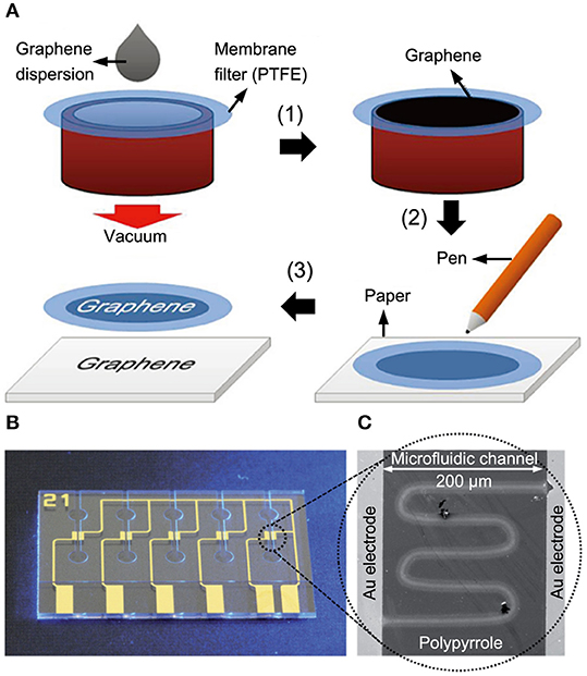
Figure 1. Making graphene circuit on paper substrate via vacuum filtration method. The graphene dispersion is filtered by a PTFE membrane (A1), and the membrane filter is turned over and put on a paper, and a circuit is drawn on the back of the membrane filter with a pen (A2), and the membrane filter is removed from the paper substrate and the target is formed (A3), and the image of a microfluidic chip is fabricated on a quartz glass wafer (B), and scanning electron microscopy (SEM) image of polypyrrole pattern is written with a laser between the gold electrodes (C). Reproduced with permissions from Hyun et al. (2013). Copyright 2013, Wiley-VCH. Reproduced with permissions from Agarwal et al. (2017). Copyright 2017, Royal Society of Chemistry.
Polymer conductive inks include poly (3,4-ethylenedioxythiophene) /poly(styrenesulfonate) (PEDT/PSS), polyaniline (PAN), polythiophene, polypyrrole (PPy), and so on. The corresponding printing methods can be direct writing (Aydemir et al., 2013), dip-pen nanolithography (Piner et al., 1999; Salaita et al., 2007), e-beam nanolithography (Yun et al., 2004), inkjet printing (Yoshioka and Jabbour, 2006; Yun et al., 2011), electrohydrodynamic printing (Chang et al., 2018), etc. Figures 1B,C show a conducting polymer pattern with direct laser writing method. A microfluidic chip with gold electrodes in the channel is fabricated first on a quartz glass substrate, and then the aqueous solution of pyrrole-3-carboxylic acid is injected in the microfluidic channel. Finally, a conductive polymer pattern with micro/nano structures in the aqueous solution is drawn by using a femtosecond laser (Agarwal et al., 2017).
Typical metal-based conductive inks include metal (e.g., Au, Ag, Pt, Cu) nanoparticle dispersion and metal compound precursor solution. Among them, Ag-based nanoink has gained special research interest due to its moderate price compared with Au and Pt (Lee et al., 2005; Rao et al., 2015), as well as its high electrical conductivity after sintering (Kwon et al., 2018; Glier et al., 2019). The typical sintering process lasts for up to 60 min at heating temperatures ranging between 125 and 250°C, which limits the practical applications of the Ag-based nanoink on heat-sensitive flexible substrates (Mou et al., 2018). In recent years, infrared (NIR) sintering technology (Tobjork et al., 2012) has been widely used in flexible electronics, which greatly shortens the sintering time. The Ag nanoink could be selectively heated without substrate deformation due to the low NIR absorption of the polymer substrate (Gu et al., 2018). Figure 2A presents the conductivity variation of Ag nanoparticles (AgNP) sintered by NIR with the cross-sectional SEM images shown as insets of the sintered film at different sintering times. The flexible hybrid circuit presented in Figure 2B is fabricated through integrating the flexible circuit and the electrical components on a terephthalate (PET) substrate. The conductive circuit is made by screen printing, followed by sintering with NIR. Besides, Tavakoli et al. (2018) demonstrated a room temperature “sintering” method that could drastically improve the conductivity and mechanical deformability of the AgNP ink circuits printed on tattoo paper substrates. The circuit is fabricated through printing AgNP ink on tattoo substrate, followed by coating a layer of eutectic gallium-indium (EGaIn) liquid metal on the surface of the printed ink. Semisolid metal mixture composed of AgNP-Ga-In clusters surrounded by Ga-rich film is thus formed, which significantly improves the conductivity and the tolerance to tensile strain of the printed traces. Figure 2C presents a LED circuit with excellent flexibility, which is inkjet printed with AgNP-Ga-In ink on a soft brain-shaped toy.
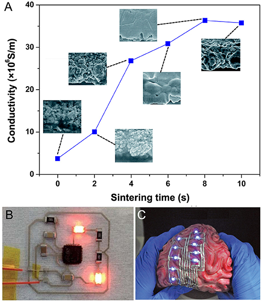
Figure 2. The conductivity of AgNP film sintered by NIR with a power of 360 kW/m2 and SEM images of the sintered film at 0, 2, 4, 6, 8, and 10 s, respectively (A), and a flexible hybrid circuit integrated electrical components and circuit screen printed with AgNP ink on a PET substrate (B), and a flexible LED circuit printed with AgNP-Ga-In ink on a soft brain-shaped toy (C). Reproduced with permissions from Gu et al. (2018). Copyright 2018, Royal Society of Chemistry. Reproduced with permissions from Tavakoli et al. (2018). Copyright 2018, Wiley-VCH.
Liquid Metal and Its Properties
Liquid metal is a newly emerging class of conductive ink. Its types and applications have been first demonstrated by Zhang et al. (2012) and it is named as DREAM ink, which is an abbreviation of direct writing of electronics based on alloy and metal ink. The melting point of such ink is typically <300°C, and room temperature liquid metal is in liquid status at room temperature and atmospheric pressure. Liquid metal has the highest electrical conductivity and the highest thermal conductivity in all the fluid materials. It attracts more and more research interest ranging from chip cooling through neural function repairment and soft robot due to its fascinating properties. There are only three kinds of pure room temperature liquid metals in nature: mercury (Hg), gallium, and cesium (Cs), with their melting point respectively at −38.87, 29.78, and 28.65°C. Liquid alloys based on these elementary metals have been fabricated for the enrichment of liquid metal family. However, there exist safety or environmental pollution issues for partial members. Mercury and low melting point amalgam cannot easily be used for safety due to the volatility of mercury. A normal person will be poisoned immediately if the mercury concentration in ambient air is larger than 1.2 mg/m3. Mercury could cause damage to human beings and environment as it goes into the biological cycle (Wood, 1974; Trasande et al., 2005; Zahir et al., 2005). Alkalis such as sodium (Na), potassium (K), and cesium (Cs) are metals with the highest activity. Spontaneous combustion or explosions will occur as they meet with water. At present, gallium and its alloys are the most studied conductive liquid metal inks due to their usage safety. Table 1 lists the physical properties of several typical liquid metals compared with that of water. It can be seen that Ga, EGaIn (75% Ga, 25% In by weight), and Ga67In20.5Sn12.5 have both metallic and fluid properties. The electrical conductivity of liquid metal is about 12 orders of magnitude higher than that of water. Its kinematic viscosity is about one third lower than that of water, indicating the good rheological property as well as the outstanding electrical property of liquid metal.
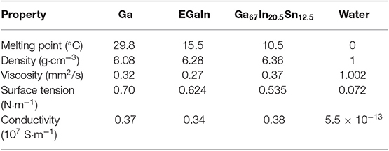
Table 1. A comparison of the physical properties between several typical liquid metals (Morley et al., 2008) and water.
The electrical conductivity of traditional conductive inks, whether it be conductive polymer system, nano-metal solution, organometallic ink or carbon conductive ink, is rather low. The electrical performance of the printed circuit will be greatly improved to the level of bulk metals after post-treatments including drying, sintering, annealing, etc. The purpose of such post processes is to remove solvent, Dispersant, and stabilizer agent in the printing ink (Tai, 2012). However, long preparation time and complicated craft of the traditional inks limit their application in rapid circuit manufacturing. Compared to these traditional inks, liquid metal has many advantages such as simple preparation and no post-treatment processes. Table 2 lists a comparison of the electrical conductivities of several typical conductive inks. It can be seen that the electrical conductivities of the conductive carbon ink and the conductive polymer are about two to three orders of magnitude lower than that of liquid metal, which impedes their application development in high-sensitivity circuits fabrication. To the metal conductive ink, post-treatments are often needed to improve the electrical conductivity, reducing the printing speed while improving the manufacturing costs. In order to obtain enhanced performance, fabrication of composite conductive inks by adding liquid metal to carbon nanotube, polymer, AgNP, and so on has become a growing trend (Koh et al., 2018; Tavakoli et al., 2018; Park et al., 2019; Wang et al., 2019).
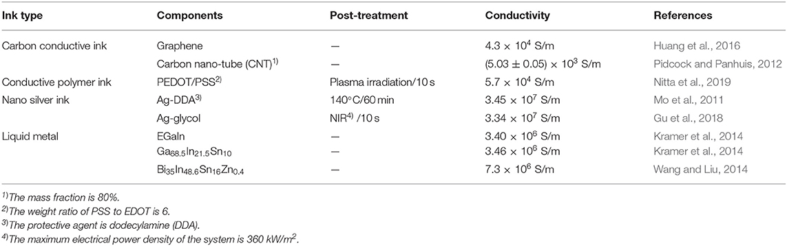
Table 2. A comparison of the electrical conductivities of several typical conductive inks.
Oxidation Characteristics of Liquid Metal
Gallium and Ga-based alloys are the representatives of room temperature liquid metal. As gallium is exposed to air, it is easy to react with oxygen to form gallium oxide, which in turn prevents gallium from further oxidation. Such characteristic of gallium is similar to that of aluminum (Regan et al., 1997). Contrary to gallium, indium is not easy to oxidize (Tostmann et al., 1999). The substance coated on the surface of Ga-based liquid alloys is mainly gallium oxide, which could increase the surface tension of the liquid metal. The oxide film could also alter the mechanical property of liquid metal, which behaves like an elastic ball in normal state and a liquid once the surface stress is larger than 0.5 N/m.
Zhang et al. (2013) disclosed that, oxidation of liquid metal played an extremely important role in realizing its printability and adhesion to various target substrates. Generally, large surface tension and poor adhesion between the liquid metal and the substrate often impede the flexible printing process including impact and spread (Figure 3A). To experimentally characterize the adhesion of the liquid metal ink, the surface tension and the contact angle of the droplets were both measured (Zhang et al., 2013). The EGaIn alloy was oxidized through constantly stirring in air at room temperature, and the quantity of oxide can be calculated by weighing the weight difference between EGaIn-based liquid metal with and without oxidization. As it is shown in Figure 3B, with the increase of oxygen content, the surface tension of the liquid metal droplet increases. Through oxidation adhesion mechanism, Zhang et al. (2013) established a generalized way for pervasively and directly printing electronics on various substrates which were expected to be significant in a wide spectrum of electrical engineering areas. In that method, the liquid metal no longer needs to be pre-oxidized to guarantee its applicability on target substrates. One critical mechanism was found as that the atomized liquid metal microdroplets could be quickly oxidized in the air due to their large specific surface area, resulting in a significant increase of the adhesive capacity and thus firm deposition of the ink to the substrate.
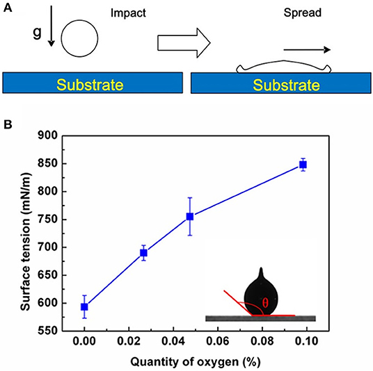
Figure 3. Impact and spread processes of a single droplet on a flat substrate surface (A), and the relation curve between the surface tension of liquid metal and the quantity of oxygen (B). The inset represents a schematic diagram of the contact angle of a liquid metal droplet. Reproduced with permissions from Zhang et al. (2013). Copyright 2013, Springer Nature.
Wettability and Conductivity of Liquid Metal
Gao et al. (2012) investigated the influence of oxidation on wettability and conductivity of the liquid metal. The liquid metal was GaIn10, while the substrate was, respectively, epoxy resin sheet, glass, plastic, silica gel sheet, paper, and cloth. It was found experimentally that with the increase of oxide content, the wettability of liquid metal was improved and the conductivity was thus reduced. Zheng et al. (2014), respectively, measured the contact angles between EGaIn droplets and polyvinylchloride (PVC) film, stainless steel, and paper substrates, respectively. It was discovered that with the increase of the applied pressure, the contact angle between EGaIn droplets and PVC reached the largest variation range. In general, PVC film serves as the best candidate substrate among the above three ones for liquid metal printing.
There is also an important relationship between the surface roughness and the wetting property of liquid metal. Kramer et al. (2014) measured the contact angles of EGaIn and Ga68.5In21.5Sn10 droplets on metal films (Si, In, and Sn, respectively) with different roughnesses. The experimental results indicated that surface roughness had a crucial impact on wettability of liquid metal droplet.
Zheng et al. (2013) investigated the electrical reliability of the lines printed on the flexible substrate. EGaIn and coated paper were selected as the ink and the substrate, respectively. The length and the width of the printed line encapsulated by room temperature vulcanizing silicone rubber (RTV) was 18 cm and 1 mm, respectively. It can be seen from the results as shown in Figure 4A that the resistivity is almost invariant as the bending angle of the substrate is respectively at −180, −90, 0, 90, and 180°. It indicates the good electrical stability of liquid metal circuit.
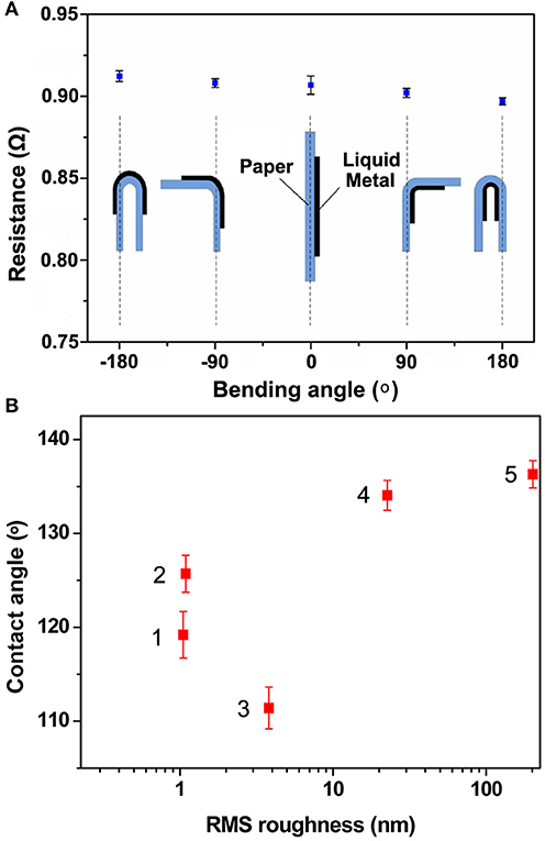
Figure 4. Resistance values of a printing wire at five different bending angles. The length and the width of the wire are 18 cm and 1 mm, respectively (A), and measured contact angles of liquid metal droplets on substrates with different RMS roughnesses. The numbers 1 to 5 represent silicone wafer, glass, PVC plastic film, PDMS and paper substrates, respectively (B). Reproduced with permissions from Zheng et al. (2013). Copyright 2013, Springer Nature. Reproduced with permissions from Wang and Liu (2015b). Copyright 2015, Royal Society of Chemistry.
Wettability between liquid metal and substrates plays a key role in determining the printing feasibility. The substrates for liquid metal printing can be various materials with different surface roughnesses. Five representative substrates were selected by Wang and Liu (2015b) to investigate the wetting property of liquid metal. They were, respectively, silicon wafer, glass, PVC plastic film, PDMS, and paper substrates, and their corresponding root mean square (RMS) roughnesses were 1.05, 1.09, 3.81, 22.6, and 202 nm, respectively. The measured mean contact angles between Galinstan (68.5% Ga, 21.5% In, 10% Sn by weight, melting point is about 11°C) and these five substrates were 119.2, 125.7, 111.4, 134.1, and 136.3°, respectively, as shown in Figure 4B. It can be seen that the contact angle value corresponding to PVC plastic film substrate is the smallest among the five ones, which indicates the good wettability between Galinstan and PVC plastic film.
Wettability between liquid metal and solid metals can be used to prepare newly conductive inks. Tang et al. (2017) fabricated a type of liquid metal-based printing ink called as transitional-state metallic mixtures (TransM2ixes) with GaIn24.5 and Cu particles. Such ink was a stable semiliquid/semisolid liquid metal amalgam containing intermetallic compound CuGa2 which was due to the reactive wetting (Kramer et al., 2014) between Ga and Cu. Addition of Cu particles remarkably enhanced the electrical conductivity (6 × 10⁶ S/m−1, ~80% increase) and the thermal conductivity [50 W/(m·K), ~100% increase] of liquid metal GaIn24.5. Figure 5A shows the image of TransM2ixes in which the packing ratio ϕ = mCu/mGaIn = 0.1. Figures 5B,C present several artistic works fabricated with TransM2ixes (ϕ = 0.1) ink on plastic, glass and silicone substrates, respectively. It indicates the potential application of TransM2ixes ink in flexible electronics.
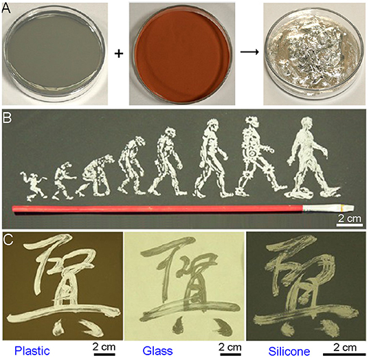
Figure 5. Images of GaIn24.5, Cu particles, and TransM2ixes (ϕ = 0.1) (A), and a piece of artistic work painted with a painting brush on plastic substrate using TransM2ixes (ϕ = 0.1) (B), and three TransM2ixes (ϕ = 0.1)-made Chinese calligraphy works written with a traditional Chinese brush on plastic, glass, and silicone substrates, respectively (C). Reproduced with permissions from Tang et al. (2017). Copyright 2017, American Chemical Society.
Liquid Metal Printing Methods
Liquid metal printing technology has its own uniqueness due to the high surface tension and the density of the ink. Zheng et al. (2014) proposed a concept of tapping mode electronic printing. The structure scheme of the printer is shown in Figure 6A. The ink storage tube is fixed at the printing driver, which is clamped on the slideway through a pulley. The printer head and the build platform can move along the X-direction and Y-direction, respectively. The printer head can be located at any position right above the build platform and its structure diagram is presented in Figure 6B. Once the printing starts, the printer head falls down to contact the substrate. Liquid metal ink disperses on the substrate with the rotating ball rolling due to the friction. At the end of printing, the printer head lifts up and leaves the substrate, for fear of destroying lines that have been printed. A flexible printed-circuit-on-board (PCB) and a printed copy of a Christmas greeting card, respectively, shown in Figures 6C,D were made in a low-cost manner through the tapping mode electronic printing technology. In 2015, such method has been developed by this lab (Yang et al., 2015) as a practical desktop personal liquid metal printer which now serves as a pervasive electronics manufacturing tool for the society. The printing resolution of the printer is <100 μm and the printing speed is preferred set in the range of 4–20 cm/s. Complex circuits or patterns with high quality can be rapidly printed out with the printer.
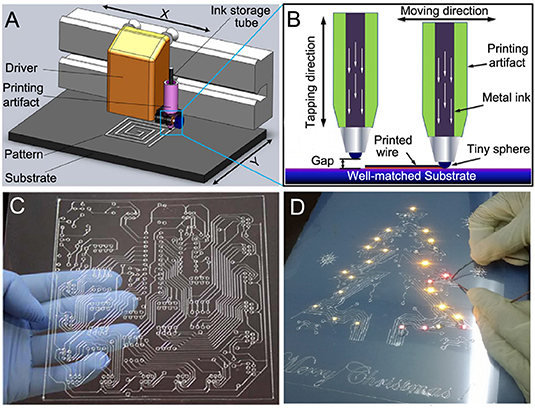
Figure 6. The structure diagram of the tapping mode electronic printing (A), and the working principle of the printer head (B), and a flexible printed PCB circuit on PVC substrate (C), and a printed copy of a Christmas greeting card (D). Reproduced with permissions from Zheng et al. (2014). Copyright 2014, Springer Nature. Reproduced with permissions from Yang et al. (2015). Copyright 2015, Higher Education Press.
Zhang et al. (2013) demonstrated a non-contact printing method named as liquid metal atomized spraying technology, which could be utilized to draw circuit on arbitrary surfaces. The principle is shown diagrammatically in Figure 7A. The printing system is mainly composed of airbrush, mask, and substrate. Liquid metal ink in the container flows into the airbrush due to gravity. Then, it is atomized into fog microdroplets under the action of high atmospheric pressure at the nozzle. Microdroplets are deposited onto the substrate surface through mask pores. Liquid metal pattern will be formed as the mask is removed. A LED circuit shown in Figure 7B is printed through this way. In addition, patterns could also be printed on leaves, rubber, and so on (Figure 7C). Suppose that a screen mask is used, complex patterns can be fabricated in short time. Such printing technique is called liquid metal screen printing (Wang and Liu, 2015b). Figure 7D presents a picture of two dragons playing with a pearl pattern printed on black paper substrate through screen printing approach. Liquid metal spray printing is becoming ripe gradually and is used for fabricating skin electronics (Guo et al., 2014; Li et al., 2016; Gui et al., 2017).
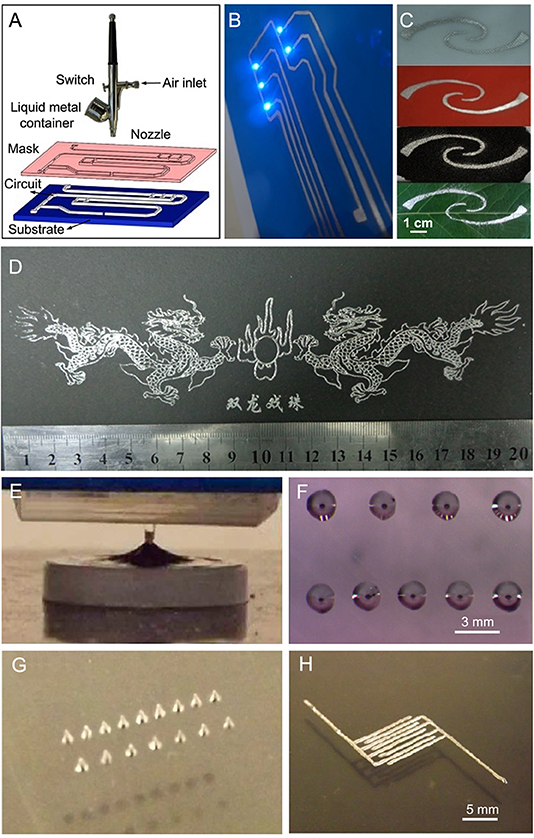
Figure 7. The schematic diagram of the atomized spraying of liquid metal (A), and a printed LED circuit (B), and conductive tracks on the surfaces of the substrates which are PVC, typing paper, porous rubber, and tree leaf, from top to bottom, respectively (C). A picture of two dragons playing with a pearl pattern printed on black paper substrate (D). Reproduced with permissions from Zhang et al. (2013). Copyright 2013, Springer Nature. Reproduced with permissions from Wang and Liu (2015b). Copyright 2015, Royal Society of Chemistry. The image of the tip of the print head contacting the liquid metal ink (E), and the printed 340-μm-diameter liquid metal droplets arranged on a silicone elastomer substrate (F,G), and a printed comb capacitor (H). Reproduced with permissions from Tabatabai et al. (2013). Copyright 2013, American Chemical Society.
Tabatabai et al. (2013) investigated a microcontact printing technique with which a liquid-phase circuit could be patterned on the substrate by using a microcontact printer. The print head is fabricated through casting PDMS, and the diameter of the hemispherical-shaped tip is 0.75 mm. Microcontact printing starts by dipping the print head into a liquid metal (EGaIn) pool and then retracting it (Figure 7E). Next, the print head wetted by liquid metal is pressed onto the substrate and thus a droplet is formed (Figures 7F,G). Repeat the process by controlling the droplet spacing distance less than the droplet diameter, and the printed droplets can form a solid line (Figure 7H) or face on the substrate. Microcontact printing provides a method of patterning circuits on arbitrary planar geometries without the need for mold or mask fabrication.
Kramer et al. (2013) introduced a masked deposition of liquid metal (Ga68.5In21.5Sn10) for fabricating liquid-embedded elastomer conductors. The schematic diagram is presented in Figure 8A. The process can be depicted as follows: glass slide, PDMS, tin foil, and PTFE photoresist are stacked in the bottom-to-top direction (1), and then tin foil is patterned with photolithography (2). Spin-coating a poly(acrylic acid) (PAA) release layer onto the elastomer surface without coating the super-hydrophobic photoresist (3), followed by sputtering indium on the surface (4). After rinsing the surface with acetone, the part on the tin foil surface is removed (5). Then, the surface is flooded with liquid metal (6), which reactively wets the tin foil (7). Excess liquid metal is removed with a thin-film scraper (8) and the remaining sputter mask is removed after rinsing the surface with water (9). Subsequently, the liquid features are cooled and encapsulated by coating with an elastomer (10). Such process incorporates liquid metal printing and photolithography, which could pattern a highly conductive liquid metal circuit within elastomer films without the need for molding, bonding, and syringe-filling (Kramer et al., 2013). The liquid-embedded elastomer shown in Figures 8B,C exhibits excellent bendability and stretchability.
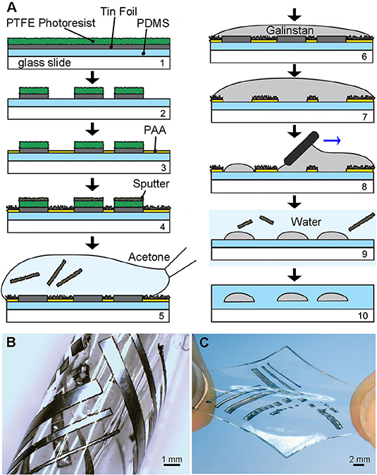
Figure 8. Schematic diagram of liquid-embedded elastomer conductor fabricated by masked deposition of Ga-In alloys (A), and a liquid-embedded elastomer in bending (B and stretching states (C), respectively, which is patterned by selectively wetting of Ga-In alloy. Reproduced with permissions from Kramer et al. (2013). Copyright 2013, Wiley-VCH.
Different from direct writing or printing of liquid metal, which is most commonly used, Wang et al. (2015) introduced an indirect printing method that is named as transfer printing. The printing process begins with fabricating a liquid metal circuit on the PVC film substrate, followed by covering liquid-phase PDMS solution over the circuit. After curing of the PDMS, the whole structure is frozen to solidify the liquid metal (EGaIn). Considering the undercooling degree of Ga-based alloys, the cooling temperature should be lower than 0°C. As the PVC film is peeled off, the liquid metal circuit is embedded in the PDMS. Then, electronic components such as electronic chips, resistors, and capacitors are assembled on the circuit according to the circuit diagram. After encapsulating the transfer printed electronics with additional PDMS, a flexible liquid metal circuit is finally fabricated. Figure 9A shows the schematic diagram of the liquid metal transfer printing process. Figure 9B shows a printed complex liquid metal circuit encapsulated by PDMS with the thickness of 300 μm. The liquid metal circuit maintains an electrical connection as the PDMS substrate is stretched up to 130% of the original length, which indicates the good flexibility of the circuit. Figure 9C presents a printed wristband circuit in working state that exhibits its truly wearable characteristics.
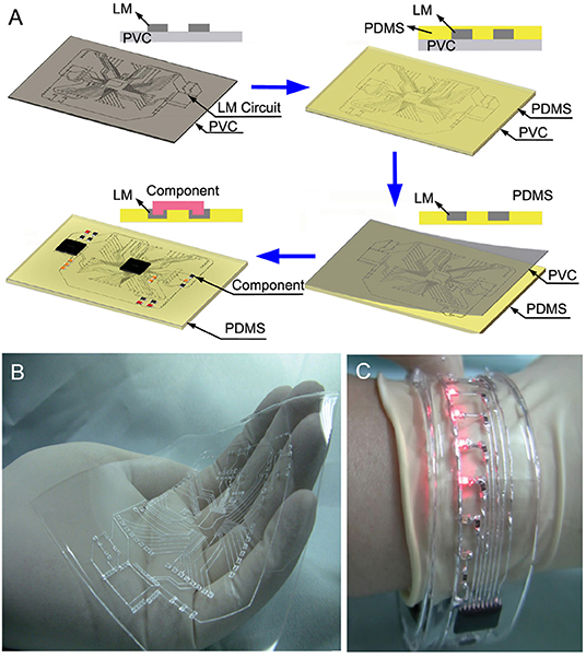
Figure 9. Schematic illustration of liquid metal transfer printing fabrication process (A), and a printed flexible liquid metal functional circuit encapsulated with PDMS (B), and a printed wristband circuit in working state (C). Reproduced with permissions from Wang et al. (2015). Copyright 2015, Wiley-VCH.
Lu et al. (2017) demonstrated the liquid metal corrosion sculpture method for fabricating complex patterns on Al substrate. The schematic diagram of fabrication is shown in Figure 10A. A plastic mask with hollow pattern is placed on the Al substrate closely, and liquid metal (GaIn10) microdroplets generated by an airbrush are sprayed uniformly on the substrate. Al substrate will be in direct contact with liquid metal through the hollow space on the mask. Al-Ga metal solution will be formed at the interface between Al substrate and liquid metal. After a few minutes to several hours of removing the plastic mask and cleaning Al plates with alcohol, in order to obtain different corrosion depths, a sculptured pattern is thus formed on the substrate. Figures 10B–E present several patterns fabricated with such approach. Compared to traditional ceramic machining techniques, the liquid metal sculpture method has several advantages including high productivity, low cost, and good surface smoothness (Lu et al., 2017).
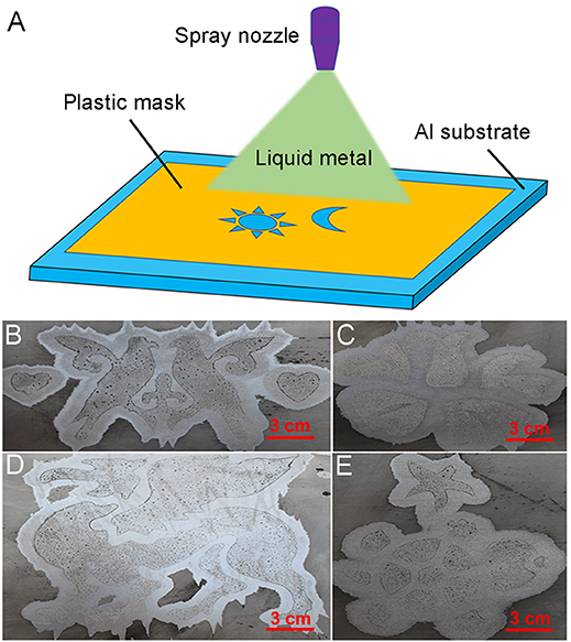
Figure 10. Schematic diagram of liquid metal corrosion sculpture method (A), and four different patterns printed on Al substrates with liquid metal corrosion sculpture method (B–E). Reproduced with permissions from Lu et al. (2017). Copyright 2017, Science China Press and Springer Nature.
Liu et al. (2018) introduced laser sintering method to print flexible electronics by selectively coalescing liquid metal nanoparticles. First of all, fabricate a 10-μm-thick nanoparticle film on the substrate through spray-printing liquid metal (EGaIn) nanoparticle inks. As a thin oxide skin could spontaneously form on the surface of Ga-based liquid metal exposed to air, these EGaIn nanoparticles are electrically insulated due to their oxide skins. Then, an ytterbium pulsed fiber laser is used to scan the nanoparticle film and the oxide skins are selectively ruptured and ablated. EGaIn nanoparticles are therefore coalesced to form a conductive line. Figure 11A presents the schematic diagram of laser sintering method, and Figure 11B shows a soft electronic circuit with intricate pattern fabricated directly onto an elastomer substrate which is adhered to a human wrist. It indicates the application potential of liquid metal laser sintering in wearable electronics. Figure 11C shows a printed gear pattern, and Figure 11D presents a comparison of the surface morphology between unsintered and sintered regions of the pattern. It can be seen that particles in the unsintered region remain spherical, while particles in the sintered region coalesce into a connected network. Laser sintering of liquid metal nanoparticles demonstrates a rapid approach for printing high-resolution flexible electronics.
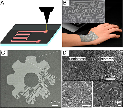
Figure 11. Schematic diagram of laser sintering method of liquid metal nanoparticles (A), and a soft circuit board printed on a biocompatible substrate adhered to the wrist (B), and the image of a laser-sintered gear (C), and the SEM image of a sintered-to-unsintered region with the enlarged view (D). Reproduced with permissions from Liu et al. (2018). Copyright 2018, American Chemical Society.
In order to change the color appearance of the printed circuit, (Liang and Liu, 2018) proposed a colorful liquid metal circuit fabrication method, and the process flow diagram is presented in Figure 12A. First of all, a liquid metal (GaIn24.5) circuit on PVC or paper substrate is printed with direct desktop printing, spray printing, or screen printing method. Then, the circuit is solidified by placing it in a refrigerator for more than 2 h, followed by screen printing or direct writing (using a brush or a porous needle pen) the liquid pigments on the surface of the conductive wires at about 0°C. After the colorful liquid metal has dried naturally, it is packaged with PDMS solution. With this method, circuits or conductive patterns with various colors can be conveniently prepared (Figures 12B–D).
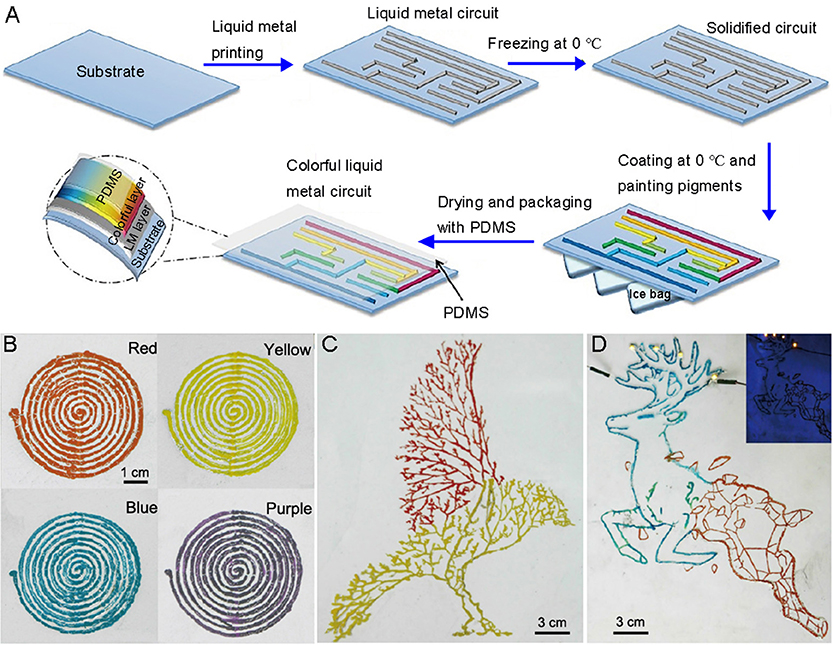
Figure 12. Schematic diagram of colorful liquid metal circuit fabrication process (A), and Ga-based liquid metal inductance coil with different colors (B), and liquid metal color image of eagle pattern (C), and liquid metal color image of deer pattern, top right inset is the photo of the pattern after electrifying (D). Reproduced with permissions from Liang and Liu (2018). Copyright 2018, Science China Press and Springer Nature.
Guo et al. (2019b) proposed a semi-liquid metal and adhesion–selection enabled rolling and transfer (SMART) printing method. Ni-EGaIn is selected as liquid metal ink, which is in semi-liquid state. The preparation process of a flexible circuit begins with printing the predesigned pattern on a thermal transfer paper with the PU glue by using a laser printer, followed by, printing Ni-EGaIn ink on the paper with the toner pattern by a roller. As the adhesion between Ni-EGaIn and toner is negligible in comparison to that between Ni-EGaIn and PU glue, the Ni-EGaIn ink is selectively printed on the PU glue part of the transfer paper. Subsequently, the liquid metal pattern is transfer printed by attaching the pattern side of the transfer paper to the surface of ecoflex substrate with a pressure of about 2.5 kPa. Finally, the liquid metal pattern on the ecoflex substrate is packaged by printing mixed ecoflex 00-30, which could cure in 15 min at room temperature. The whole process is indicated in Figure 13A, and a printed LED array flexible circuit on paper substrate is shown in Figure 13B. The preparation time of a circuit with SMART printing is typically within 30 min, which is less than other liquid metal printing methods such as direct writing, spray printing, and so on (Guo et al., 2019a). This method provides a super-fast way for fabricating soft electronics.
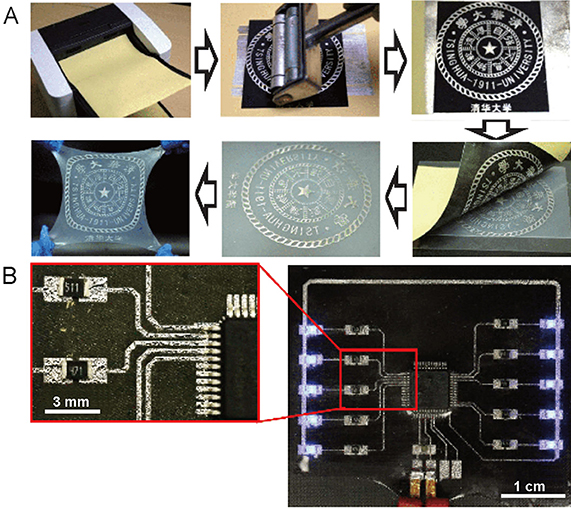
Figure 13. The preparation process of liquid metal pattern with rolling and transfer printing method (A), and a printed LED array flexible circuit on paper substrate (B). Reproduced with permissions from Guo et al. (2019b). Copyright 2019, Science China Press and Springer Nature.
Prospect
Conclusively, printed electronics, which means instant manufacturing, has become a research focus in recent years. The potential applications cover from consumer electronics to energy, medical, and so on. Various kinds of liquid metal printing methods have emerged in succession and are in ascendance. The substrates used for printing can be paper, plastic, metal surface, cloth, or even skin (Rogers, 2017; Wang et al., 2018). Among the factors affecting the printing effect, the ink is the most important one. As to the newly liquid metal printing ink, the way to increase ink types lies in developing more and more low melting point alloys or liquid metal-based conductive composites. (Wang and Liu, 2013) has put forward the concept of liquid metal material genome initiative, which is aimed to discover advanced functional alloys with low melting point with the help of physical and chemical methods. Liquid metal family can be expanded through reorganization of existing elemental metals or alloys. High-throughput calculation, preparation, and characterization techniques can be fully tried to screen out suitable liquid metal ink, which has desired properties including electrical conductivity, viscosity, wettability, oxidation property, and so on. Based on the various selectable inks, brand new kinds of printing techniques of liquid metal can also be further developed. In addition, it can be seen from the numerous literatures that electronic device printing (Andrews et al., 2018; Choi et al., 2019) is becoming one of the most important direction in flexible electronics. Liquid metal-based circuit printing including devices and conductive wires could provide a powerful strategy for the establishment of future smart homes (Wang and Liu, 2015a).
Author Contributions
LW finished this review, including writing and formatting of the manuscript. JL revised the manuscript and made important supplementary.
Funding
This work was partially supported by the National Science Foundation for Young Scientists of China (Grant No. 51706234) and CAS Key Laboratory of Cryogenics, Technical Institute of Physics and Chemistry (CRYOQN201909).
Conflict of Interest
The authors declare that the research was conducted in the absence of any commercial or financial relationships that could be construed as a potential conflict of interest.
References
Agarwal, N., Ryu, H., Mangang, M., Pfleging, W., and Kim, J. (2017). Direct writing of a conducting polymer pattern in aqueous solution by using an ultrashort laser pulse. RSC Adv. 7, 38565–38569. doi: 10.1039/C7RA05195F
Andrews, J. B., Mondal, K., Neumann, T. V., Cardenas, J. A., Wang, J., Parekh, D. P., et al. (2018). Patterned liquid metal contacts for printed carbon nanotube transistors. ACS Nano 12, 5482–5488. doi: 10.1021/acsnano.8b00909
Aydemir, N., Parcell, J., Laslau, C., Nieuwoudt, M., Williams, D. E., and Travas-Sejdic, J. (2013). Direct writing of conducting polymers. Macromol. Rapid Commun. 34, 1296–1300. doi: 10.1002/marc.201300386
Chang, J. K., He, J. K., Lei, Q., and Li, D. C. (2018). Electrohydrodynamic printing of microscale PEDOT:PSS-PEO features with tunable conductive/thermal properties. ACS Appl. Mater. Interfaces 10, 19116–19112. doi: 10.1021/acsami.8b04051
Chen, T. H., Yeh, Y. C., and Liao, Y. C. (2018). Healable and foldable carbon nanotube/wax conductive composite. ACS Appl. Mater. Interfaces 10, 24217–24223. doi: 10.1021/acsami.8b08310
Choi, S., Kim, K. T., Park, S. K., and Kim, Y. H. (2019). High-Mobility Inkjet-Printed Indium-Gallium-Zinc-Oxide thin-film transistors using Sr-Doped Al2O3 gate dielectric. Materials 12:852. doi: 10.3390/ma12060852
Coleman, J. N., Lotya, M., O'Neill, A., Bergin, S. D., King, P. J., Khan, U., et al. (2011). Two-dimensional nanosheets produced by liquid exfoliation of layered materials. Science 331, 568–571. doi: 10.1126/science.1194975
Cui, Z. (2019). Printing practice for the fabrication of flexible and stretchable electronics. Sci. China Technol. Sci. 62, 224–232. doi: 10.1007/s11431-018-9388-8
Gao, W., Ota, H., Kiriya, D., Takei, K., and Javey, A. (2019). Flexible electronics toward wearable sensing. Acc. Chem. Res. 52, 523–533. doi: 10.1021/acs.accounts.8b00500
Gao, Y. X., Li, H. Y., and Liu, J. (2012). Direct writing of flexible electronics through room temperature liquid metal ink. PLoS ONE 7:e45485. doi: 10.1371/journal.pone.0045485
Glier, T. E., Akinsinde, L., Paufler, M., Otto, F., Hashemi, M., Grote, L., et al. (2019). Functional printing of conductive silver-nanowire photopolymer composites. Sci. Rep. 9:6465. doi: 10.1038/s41598-019-42841-3
Gu, W. B., Yuan, W., Zhong, T., Wu, X. Z., Zhou, C. S., Lin, J., et al. (2018). Fast near infrared sintering of silver nanoparticle ink and applications for flexible hybrid circuits. RSC Adv. 8, 30215–30222. doi: 10.1039/C8RA04468F
Gui, H., Tan, S. C., Wang, Q., Yu, Y., Liu, F. J., Lin, J., et al. (2017). Spraying printing of liquid metal electronics on various clothes to compose wearable functional device. Sci. China Technol. Sci. 60, 306–316. doi: 10.1007/s11431-016-0657-5
Guo, C. R., Yu, Y., and Liu, J. (2014). Rapidly patterning conductive components on skin substrates as physiological testing devices via liquid metal spraying and pre-designed mask. J. Mater. Chem. B 2, 5739–5745. doi: 10.1039/C4TB00660G
Guo, R., Sun, X. Y., Yuan, B., Wang, H. Z., and Liu, J. (2019a). Magnetic liquid metal (Fe-EGaIn) based multifunctional electronics for remote self-healing materials, degradable electronics, and thermal transfer printing. Adv. Sci. 6:1901478. doi: 10.1002/advs.201901478
Guo, R., Yao, S. Y., Sun, X. Y., and Liu, J. (2019b). Semi-liquid metal and adhesion-selection enabled rolling and transfer (SMART) printing: a general method towards fast fabrication of flexible electronics. Sci. China Mater. 62, 982–994. doi: 10.1007/s40843-018-9400-2
Huang, X. J., Leng, T., Chang, K. H., Chen, J. C., Novoselov, K. S., and Hu, Z. R. (2016). Graphene radio frequency and microwave passive components for low cost wearable electronics. 2D Mater. 3:025021. doi: 10.1088/2053-1583/3/2/025021
Hyun, W. J., Park, O. O., and Chin, B. D. (2013). Foldable graphene electronic circuits based on paper substrates. Adv. Mater. 25, 4729–4734. doi: 10.1002/adma.201302063
Ji, A., Chen, Y. M., Wang, X. Y., and Xu, C. Y. (2018). Inkjet printed flexible electronics on paper substrate with reduced graphene oxide/carbon black ink. J. Mater. Sci Mater. Electr. 29, 13032–13042. doi: 10.1007/s10854-018-9425-1
Kamyshny, A., and Magdassi, S. (2019). Conductive nanomaterials for 2D and 3D printed flexible electronics. Chem. Soc. Rev. 48, 1712–1740. doi: 10.1039/C8CS00738A
Karagiannidis, P. G., Hodge, S. A., Lombardi, L., Tomarchio, F., Decorde, N., Milana, S., et al. (2017). Microfluidization of graphite and formulation of graphene-based conductive inks. ACS Nano 11, 2742–2755. doi: 10.1021/acsnano.6b07735
Karim, N., Afroj, S., Tan, S. R., Novoselov, K. S., and Yeates, S. G. (2019). All inkjet-printed graphene-silver composite ink on textiles for highly conductive wearable electronics applications. Sci. Rep. 9:8035. doi: 10.1038/s41598-019-44420-y
Khan, S., Ali, S., and Bermak, A. (2019). Recent developments in printing flexible and wearable sensing electronics for healthcare applications. Sensors 19:1230. doi: 10.3390/s19051230
Kim, T. S., Lee, Y., Xu, W. T., Kim, Y. H., Kim, M., Min, S. Y., et al. (2019). Direct-printed nanoscale metal-oxide-wire electronics. Nano Energy 58, 437–446. doi: 10.1016/j.nanoen.2019.01.052
Koh, A., Sietins, J., Slipher, G., and Mrozek, R. (2018). Deformable liquid metal polymer composites with tunable electronic and mechanical properties. J. Mater. Res. 33, 2443–2453. doi: 10.1557/jmr.2018.209
Kramer, R. K., Boley, J. W., Stone, H. A., Weaver, J. C., and Wood, R. J. (2014). Effect of microtextured surface topography on the wetting behavior of eutectic gallium-indium alloys. Langmuir 30, 533–539. doi: 10.1021/la404356r
Kramer, R. K., Majidi, C., and Wood, R. J. (2013). Masked deposition of gallium-indium alloys for liquid-embedded elastomer conductors. Adv. Funct. Mater. 23, 5292–5296. doi: 10.1002/adfm.201203589
Kwon, J., Suh, Y. D., Lee, J., Lee, P., Han, S., Hong, S., et al. (2018). Recent progress in silver nanowire based flexible/wearable optoelectronics. J. Mater. Chem. C 6, 7445–7461. doi: 10.1039/C8TC01024B
Lee, H. H., Chou, K. S., and Huang, K. C. (2005). Inkjet printing of nanosized silver colloids. Nanotechnology 16, 2436–2441. doi: 10.1088/0957-4484/16/10/074
Li, J., Guo, C. R., Wang, Z. S., Gao, K., Shi, X. D., and Liu, J. (2016). Electrical stimulation towards melanoma therapy via liquid metal printed electronics on skin. Clin. Transl. Med. 5:21. doi: 10.1186/s40169-016-0102-9
Liang, S. T., and Liu, J. (2018). Colorful liquid metal printed electronics. Sci. China Technol. Sci. 61, 110–116. doi: 10.1007/s11431-017-9116-9
Liu, S. L. Z., Yuen, M. C., White, E. L., Boley, J. W., Deng, B. W., Cheng, G. J., et al. (2018). Laser sintering of liquid metal nanoparticles for scalable manufacturing of soft and flexible electronics. ACS Appl. Mater. Interfaces 10, 28232–28241. doi: 10.1021/acsami.8b08722
Lu, J. R., Yi, L. T., Wang, L., Tan, S. C., Gui, H., and Liu, J. (2017). Liquid metal corrosion sculpture to fabricate quickly complex patterns on aluminum. Sci. China Technol. Sci. 60, 65–70. doi: 10.1007/s11431-016-0433-9
Mo, L. X., Liu, D. Z., Li, W., Li, L. H., Wang, L. C., and Zhou, X. Q. (2011). Effects of dodecylamine and dodecanethiol on the conductive properties of nano-Ag films. Appl. Surf. Sci. 257, 5746–5753. doi: 10.1016/j.apsusc.2011.01.090
Mohammed, M. G., and Kramer, R. (2017). All-printed flexible and stretchable electronics. Adv. Mater. 29:1604965. doi: 10.1002/adma.201604965
Morales-Narvaez, E., Baptista-Pires, L., Zamora-Galvez, A., and Merkoci, A. (2017). Graphene-based biosensors: going simple. Adv. Mater. 29:1604905. doi: 10.1002/adma.201604905
Morley, N. B., Burris, J., Cadwallader, L. C., and Nornberg, M. D. (2008). GaInSn usage in the research laboratory. Rev. Sci. Instrum. 79:056107. doi: 10.1063/1.2930813
Mou, Y., Zhang, Y. R., Cheng, H., Peng, Y., and Chen, M. X. (2018). Fabrication of highly conductive and flexible printed electronics by low temperature sintering reactive silver ink. Appl. Surf. Sci. 459, 249–256. doi: 10.1016/j.apsusc.2018.07.187
Nitta, K., Tsumaki, M., Kawano, T., Terashima, K., and Ito, T. (2019). Printing PEDOT from EDOT via plasma-assisted inkjet printing. J. Phys. D Appl. Phys. 52:315202. doi: 10.1088/1361-6463/ab1ef2
Park, Y. G., Min, H., Kim, H., Zhexembekova, A., Lee, C. Y., and Park, J. U. (2019). Three-dimensional, high-resolution printing of carbon nanotube/liquid metal composites with mechanical and electrical reinforcement. Nano Lett. 19, 4866–4872. doi: 10.1021/acs.nanolett.9b00150
Pidcock, G. C., and Panhuis, M. I. H. (2012). Extrusion printing of flexible electrically conducting carbon nanotube networks. Adv. Funct. Mater. 22, 4790–4800. doi: 10.1002/adfm.201200724
Piner, R. D., Zhu, J., Xu, F., Hong, S. H., and Mirkin, C. A. (1999). “Dip-pen” nanolithography. Science 283, 661–663. doi: 10.1126/science.283.5402.661
Qiu, X. B., Zhao, X. M., Liu, F. X., Chen, S. L., Xu, J. F., and Chen, G. H. (2019). Surfactant-free carbon black@graphene conductive ink for flexible electronics. J. Mater. Sci. 54, 11157–11167. doi: 10.1007/s10853-019-03687-2
Rao, R. V. K., Abhinav, K. V., Karthik, P. S., and Singh, S. P. (2015). Conductive silver inks and their applications in printed and flexible electronics. RSC Adv. 5, 77760–77790. doi: 10.1039/C5RA12013F
Regan, M. J., Tostmann, H., Pershan, P. S., Magnussen, O. M., DiMasi, E., Ocko, B. M., et al. (1997). X-ray study of the oxidation of liquid-gallium surfaces. Phys. Rev. B 55, 10786–10790. doi: 10.1103/PhysRevB.55.10786
Rogers, J. A. (2017). Wearable electronics nanomesh on-skin electronics. Nat. Nanotechnol. 12, 839–840. doi: 10.1038/nnano.2017.150
Salaita, K., Wang, Y. H., and Mirkin, C. A. (2007). Applications of dip-pen nanolithography. Nat. Nanotechnol. 2, 145–155. doi: 10.1038/nnano.2007.39
Shan, J. (2013). Preparation and film formation investigation of copper based particle-free conductive ink [Doctoral dissertation]. Tianjin University, Tianjin, China.
Tabatabai, A., Fassler, A., Usiak, C., and Majidi, C. (2013). Liquid-phase gallium-indium alloy electronics with microcontact printing. Langmuir 29, 6194–6200. doi: 10.1021/la401245d
Tai, Y. L. (2012). Preparation and application of conductive ink for printed electronics [Doctoral dissertation]. Fudan University, Shanghai, China.
Tang, J. B., Zhao, X., Li, J., Guo, R., Zhou, Y., and Liu, J. (2017). Gallium-based liquid metal amalgams: transitional-state metallic mixtures (TransM(2)ixes) with enhanced and tunable electrical, thermal, and mechanical properties. ACS Appl. Mater. Inter. 9, 35977–35987. doi: 10.1021/acsami.7b10256
Tavakoli, M., Malakooti, M. H., Paisana, H., Ohm, Y., Marques, D. G., Lopes, P. A., et al. (2018). EGaIn-assisted room-temperature sintering of silver nanoparticles for stretchable, inkjet-printed, thin-film electronics. Adv. Mater. 30:1801852. doi: 10.1002/adma.201801852
Tobjork, D., Aarnio, H., Pulkkinen, P., Bollstrom, R., Maattanen, A., Ihalainen, P., et al. (2012). IR-sintering of ink-jet printed metal-nanoparticles on paper. Thin Solid Films 520, 2949–2955. doi: 10.1016/j.tsf.2011.10.017
Tostmann, H., DiMasi, E., Pershan, P. S., Ocko, B. M., Shpyrko, O. G., and Deutsch, M. (1999). Surface structure of liquid metals and the effect of capillary waves: X-ray studies on liquid indium. Phys. Rev. B 59, 783–791. doi: 10.1103/PhysRevB.59.783
Tran, T. S., Dutta, N. K., and Choudhury, N. R. (2018). Graphene inks for printed flexible electronics: graphene dispersions, ink formulations, printing techniques and applications. Adv. Colloid Interface 261, 41–61. doi: 10.1016/j.cis.2018.09.003
Trasande, L., Landrigan, P. J., and Schechter, C. (2005). Public health and economic consequences of methyl mercury toxicity to the developing brain. Environ. Health Perspect. 113, 590–596. doi: 10.1289/ehp.7743
Wang, H. Z., Yao, Y. Y., He, Z. Z., Rao, W., Hu, L., Chen, S., et al. (2019). A highly stretchable liquid metal polymer as reversible transitional insulator and conductor. Adv. Mater. 31:e1901337. doi: 10.1002/adma.201901337
Wang, L., and Liu, J. (2013). Liquid metal material genome: initiation of a new research track towards discovery of advanced energy materials. Front. Energy 7, 317–332. doi: 10.1007/s11708-013-0271-9
Wang, L., and Liu, J. (2014). Printing low melting point alloy ink to directly make solidified circuit or functional device with heating pen. Proc. Math. Phys Eng. Sci. 470:20140609. doi: 10.1098/rspa.2014.0609
Wang, L., and Liu, J. (2015a). Ink spraying based liquid metal printed electronics for directly making smart home appliances. ECS J. Solid State Sci. 4, P3057–P3062. doi: 10.1149/2.0111504jss
Wang, L., and Liu, J. (2015b). Pressured liquid metal screen printing for rapid manufacture of high resolution electronic patterns. RSC Adv. 5, 57686–57691. doi: 10.1039/C5RA10295B
Wang, Q., Yu, Y., Yang, J., and Liu, J. (2015). Fast fabrication of flexible functional circuits based on liquid metal dual-trans printing. Adv. Mater. 27, 7109–7116. doi: 10.1002/adma.201502200
Wang, S. H., Xu, J., Wang, W. C., Wang, G. J. N., Rastak, R., Molina-Lopez, F., et al. (2018). Skin electronics from scalable fabrication of an intrinsically stretchable transistor array. Nature 555, 83–88. doi: 10.1038/nature25494
Wang, X. L., and Liu, J. (2016). Recent advancements in liquid metal flexible printed electronics: properties, technologies, and applications. Micromachines 7:206. doi: 10.3390/mi7120206
Wood, J. M. (1974). Biological cycles for toxic elements in the environment. Science 183, 1049–1052. doi: 10.1126/science.183.4129.1049
Yang, J., Yang, Y., He, Z. Z., Chen, B. W., and Liu, J. (2015). A personal desktop liquid-metal printer as a pervasive electronics manufacturing tool for society in the near future. Engineering 1, 506–512. doi: 10.15302/J-ENG-2015042
Yoshioka, Y., and Jabbour, G. E. (2006). Desktop inkjet printer as a tool to print conducting polymers. Synthetic Metals 156, 779–783. doi: 10.1016/j.synthmet.2006.03.013
Yun, M. H., Myung, N. V., Vasquez, R. P., Lee, C. S., Menke, E., and Penner, R. M. (2004). Electrochemically grown wires for individually addressable sensor arrays. Nano Lett. 4, 419–422. doi: 10.1021/nl035069u
Yun, Y. H., Lee, B. K., Choi, J. S., Kim, S., Yoo, B., Kim, Y. S., et al. (2011). A glucose sensor fabricated by piezoelectric inkjet printing of conducting polymers and bienzymes. Anal. Sci. 27, 375–379. doi: 10.2116/analsci.27.375
Zahir, F., Rizwi, S. J., Haq, S. K., and Khan, R. H. (2005). Low dose mercury toxicity and human health. Environ. Toxicol. Phar. 20, 351–360. doi: 10.1016/j.etap.2005.03.007
Zhang, Q., Gao, Y. X., and Liu, J. (2013). Atomized spraying of liquid metal droplets on desired substrate surfaces as a generalized way for ubiquitous printed electronics. Appl. Phys. A Mater. 116, 1091–1097. doi: 10.1007/s00339-013-8191-4
Zhang, Q., Zheng, Y., and Liu, J. (2012). Direct writing of electronics based on alloy and metal ink (DREAM ink): a newly emerging area and its impact on energy, environment and health sciences. Front. Energy 6, 311–340. doi: 10.1007/s11708-012-0214-x
Zheng, Y., He, Z. Z., Gao, Y. X., and Liu, J. (2013). Direct desktop printed-circuits-on-paper flexible electronics. Sci. Rep. 3:1786. doi: 10.1038/srep01786
Keywords: printed electronics, conductive ink, liquid metal, oxidation, wettability, electrical conductivity
Citation: Wang L and Liu J (2019) Advances in the Development of Liquid Metal-Based Printed Electronic Inks. Front. Mater. 6:303. doi: 10.3389/fmats.2019.00303
Received: 10 December 2018; Accepted: 13 November 2019;
Published: 03 December 2019.
Edited by:
John Zhanhu Guo, University of Tennessee, Knoxville, United StatesReviewed by:
Geza Toth, VTT Technical Research Centre of Finland Ltd, FinlandZhi-Zhu He, China Agricultural University (CAU), China
Copyright © 2019 Wang and Liu. This is an open-access article distributed under the terms of the Creative Commons Attribution License (CC BY). The use, distribution or reproduction in other forums is permitted, provided the original author(s) and the copyright owner(s) are credited and that the original publication in this journal is cited, in accordance with accepted academic practice. No use, distribution or reproduction is permitted which does not comply with these terms.
*Correspondence: Lei Wang, bHdhbmcyMDE1QG1haWwuaXBjLmFjLmNu; Jing Liu, amxpdUBtYWlsLmlwYy5hYy5jbg==