 Helena Fridman
 Liang Tian
 Karam Shreteh
 Michael Volokh
 Taleb Mokari
- Department of Chemistry and Ilse Katz Institute for Nanoscale Science and Technology, Ben-Gurion University of the Negev, Beer-Sheva, Israel
Two-dimensional CdS-based hybrid nanostructures are intriguing materials with an application prospect in different fields such as sensing (i. e., photoresistors) and solar energy harvesting (photocatalysis, photovoltaics, and so forth). We report herein a colloidal synthetic path for interfacing metal and semiconductor with 2D CdS nanoplates. Selective growth of Au, Pt, and a PtNi alloy as well as Cu2−xS semiconductor is achieved on CdS nanoplates using controlled reduction of metallic precursors and thermal decomposition of a metal-sulfide single-source precursor using standard organic-phase colloidal chemistry.
Introduction
Materials on the nanoscale with increasing complexity, and specifically hybrid nanostructures (HNSs), pose an opportunity for the rational design of novel advanced materials, with unique, and multifunctional properties (Kovalenko et al., 2015). Consisting of several domains, hybrid nanoparticles (NPs) commonly possess a combination of the properties of each nanoscale component (Maynadiø et al., 2009; Costi et al., 2010; Tan et al., 2018). In some cases, synergy between the two domains allows enhancement of the original properties and even leads to novel properties that did not exist in the separate domains (Cozzoli et al., 2006; Urban et al., 2007; Shaviv and Banin, 2010). The constantly increasing knowledge in colloidal NP synthesis (e.g., formation mechanisms, size and distribution, dimensionality and shape control, composition of constituents, surface composition—ligand type, coverage, and functionality) (Carbone and Cozzoli, 2010) provides a solid ground for the design of HNSs with domains consisting of a wide range of materials such as metals (Naskar et al., 2017), metal alloys (Habas et al., 2008), metal chalcogenides (Banin et al., 2014; Flomin et al., 2017), metal oxides (Chang et al., 2017), carbon based materials (Zhi et al., 2008), and polymers (Liu et al., 2010). HNSs have been shown useful for a variety of applications such as medicinal uses (Zhang et al., 2018), photocatalysis (Tongying et al., 2012; Waiskopf et al., 2018), and other energy-related applications (Cho et al., 2019). The scientific questions alongside the proven and potential applicative knowledge result in a constant worldwide interest in novel hybrid nanostructures.
A useful general classification scheme of HNSs would be according to the formed interface, namely semiconductor–semiconductor (SC–SC) and metal–semiconductor (M–SC) systems. A SC–SC hybrid structure with rationally-designed energy band alignment can improve the optical emission (Rukenstein et al., 2012) or facilitate charge separation (Volokh et al., 2014; Li and Lian, 2018), which are beneficial for photoluminescence or photoelectronic devices [such as photoelectrochemical cells (Chu et al., 2017; Volokh et al., 2019) and photovoltaics (Carey et al., 2015), respectively]. Maybe the most common SC–SC HNS is a core–shell structure, such as CdSe–CdS (Brovelli et al., 2011), CdSe–ZnS (Yu et al., 2005), or PbS–CdS (Zhang et al., 2016), which can enhance the fluorescence efficiency and create prototype quantum-confined structures as the quantum dot/quantum well-system. Moreover, a second material can also be grown selectively on the higher-reactivity tips of anisotropic nanocrystals. For example, EuS particle on one or both tips of CdS nanorods (Mirkovic et al., 2011) and selective growth of CdTe on CdS (Milliron et al., 2004) or PbSe on CdS and CdSe nanorods (Kudera et al., 2005).
Hybrid systems consisting of a M–SC configuration gained significant interest owing to their efficient light induced charge separation—an important property for photocatalysis-based applications (Khan et al., 2015), with the metal serving as an electron sink and possibly a reduction catalyst. In addition, some noble metal NPs such as gold, silver, and platinum have strong localized surface plasmon resonance effects (Lee et al., 2011), which is useful for sensors and photocatalysis. Additional uses include serving as anchor points for electrical connections and self-assembly of the semiconductor component of the M–SC hybrids (Kaltwasser et al., 2018; Marcovici et al., 2018), and impact on improved electronic transport (Mahler et al., 2016). During the last decade, an impressive control over the shape, composition, and complexity of the discussed above systems have been gained, and nanostructures such as disk-type Cu2S nanocrystals with Au core (Kim et al., 2010), CdSe/CdS tetrapods with one Au tip and three Ag2S tips (Mishra et al., 2012) were synthesized. Furthermore, tremendous progress has been made with metal alloys such as PtNi and PtCo in recent years, where composition tuning determines physical and chemical properties (Paulus et al., 2002; Loukrakpam et al., 2011; Cui et al., 2012).
During the last decade, colloidal (quasi) two-dimensional (2D) nanoplates or nanoplatelets (NPLs) have attracted much attention because of their unique electronic and optical properties (Ithurria et al., 2011a,b; Nasilowski et al., 2016; Kelestemur et al., 2017; Akkerman et al., 2019; Ganguly et al., 2019). At present, the research on 2D colloidal semiconductors is thriving, with various compositions (Wang et al., 2014; Berends et al., 2018; Akkerman et al., 2019; Dufour et al., 2019) and nanoscale interfaces are explored including van der Waals heterostructures, core–shell, and core–crowns in the case of SC–SC (Davis et al., 2019; Li et al., 2019; Min et al., 2019; Saidzhonov et al., 2019) and various decoration locations and amounts in the case of SC–M. Of note is the ability of metal ions to induce shape control as well as determine final composition (e.g., CuS–Ag2S or Ag2S–Ag; Liu et al., 2018). Among the II-VI nanomaterials, and cadmium chalcogenides (Kormilina et al., 2017; Li and Lian, 2018) in particular, CdS is explored due to its controllable morphology, electronic structure, and optical properties. Thus far, some metal– and semiconductor−2D CdS based hybrid nanostructures were reported, such as CdS-CdSe–Au (Chauhan et al., 2016; Das et al., 2016; Naskar et al., 2017), CdS–Pt (Li et al., 2018), CdS–Ni (Zhukovskyi et al., 2015), CdS–Ni3C (Ma et al., 2018), CdS–MoS2 (Ma et al., 2017), and CdSe–CdS (Li et al., 2016; Feng et al., 2018). However, the research of 2D CdS based hybrid nanostructures is still very insufficient. Herein, we use 2D CdS NPLs as a substrate for selective growth of Cu2−xS semiconductor, Au and Pt metals, and PtNi metal alloy.
Experimental Details
All the described colloidal syntheses were conducted using standard air-free techniques (using a Schlenk line with N2-flow).
Materials
Diphenyl ether (DPE, 99%) and octylamine (99%) were purchased from Alfa Aesar; cadmium (II) chloride (CdCl2, >99%), copper nitrate trihydrate [Cu(NO3)2·3H2O, 99.5%], gold (III) chloride (AuCl3, 99.9%), nickel (II) acetate tetrahydrate [Ni(ac)2·4H2O, >98%], and platinum (II) acetylacetonate [Pt(acac)2, 98%] were purchased from Strem Chemicals; 1,2-dichlorobenzene (DCB, 99%), 1,2-hexadecanetdiol (HDD, 90%), n-trioctylphosphine (TOP, 90%), 1-dodecanethiol (DDT, 98%), didodecyldimethylammonium bromide (DDAB, 98%), dodecylamine (DDA, 98%), oleic acid (OA, 90%), oleylamine (OLAM, 70%), sodium diethyldithiocarbamate (99%), and elemental sulfur (99.98%) were purchased from Sigma-Aldrich. Solvents for dispersion and precipitation were purchased from Bio-Lab Chemicals: hexane (AR grade), toluene (99.7%), chloroform (amylene-stabilized, 99.9%), ethanol (absolute, 99.9%), and methanol (absolute, 99.8%). All solvents and reagents were used as received.
Synthesis of 2D CdS Nanoplates (NPLs)
2D CdS NPLs were synthesized after minimal modification of the method described by Son et al. (2012). Briefly, a Cd-octylamine and sulfur-octylamine complexes were reacted in octylamine, which served both as the surfactant and the solvent. The Cd-octylamine complex was prepared by heating CdCl2 (1.5 mmol) in octylamine (10 mL) to 120 °C for 2 h. A sulfur-octylamine complex was prepared by dissolving elemental sulfur (4.5 mmol) in octylamine (5 mL) at room temperature. The resulting reddish-to-brown solution was injected into the previously-prepared Cd-octylamine complex solution at room temperature, resulting in an immediate color change to a transparent light yellow. This solution was then slowly heated at a rate of 2 °C min−1 and aged for 48 h at the target temperature of 70 °C. As 2D CdS NPLs were formed, the solution became turbid. After the reaction terminated, NPLs were precipitated out of the solution by adding excess ethanol and centrifugation. The powdery form of 2D CdS NPLs was obtained by two additional cycles of redispersion in toluene, addition of ethanol, and centrifugation.
The final CdS precipitate was dispersed in chloroform to form a CdS NPL stock solution. The stock's concentration was calibrated for the subsequent procedures by adjusting the absorbance of a ×200 diluted sample at λ = 379 nm to 0.80 (i.e., theoretical optical density of about 160).
Synthesis of Elongated 2D CdS NPLs
Elongated 2D CdS NPLs were synthesized using the same procedure, except that target temperature of the aging was 80 °C. The stock's concentration was calibrated for the subsequent procedures by adjusting the absorbance of a ×200 diluted sample at λ = 381 nm to 0.83 (i.e., theoretical optical density of about 166).
Synthesis of Copper(II)-Bisdiethyldithiocarbamate Single-Source Precursor
The diethyldithiocarbamate salt of copper, Cu[S2CNEt2]2, was prepared according to previously published methods (Jen-La Plante et al., 2010; Rukenstein et al., 2012). The water-soluble Cu(II) salt [Cu(NO3)2·3H2O, 1.208 g, 5.00 mmol] was dissolved in 40 mL of deionized water (18.2 Ω cm resistivity, purified using a Millipore Direct-Q system). Sodium diethyldithiocarbamate (2.250 g, 10.00 mmol) was dissolved separately in 40 mL of deionized water and then slowly added to the Cu(II) solution. The precipitate was allowed to form, vacuum-filtered, dried, dissolved in hot chloroform, and finally recrystallized.
Growth of Cu2−xS on CdS NPLs
The growth of Cu2−xS on CdS was achieved by mixing CdS NPLs and the copper-sulfide single-source precursor (SSP) in DDT: 0.17 mL CdS NPL stock solution was centrifuged at 15,000 rpm (~15.6 k × g) for 5 min and then redispersed in 3.0 mL DDT alongside 6.0 mg Cu[S2CNEt2]2. The mixture was then heated to 200 °C for 5 min. The reaction was then stopped by removing the heating mantle and allowing the solution to cool to room temperature. The product was cleaned by the addition of 2 mL toluene and 2 mL ethanol, followed by 10 min centrifugation.
Growth of Cu2-xS on Elongated CdS NPLs
This synthesis is similar to the previous description of Cu2−xS on CdS, except that 0.25 mL of the elongated CdS NPLs stock solution was used.
Growth of Au on CdS NPLs
The procedure of growing Au on CdS was based on previously published work, with slight modifications (Mokari et al., 2005). In a standard procedure, 0.5 mL of a CdS stock was centrifuged at 15,000 rpm (~15.6 k × g) for 5 min to precipitate the CdS NPLs. Then, the precipitate was dispersed in 3 mL DPE and transferred to a three-neck round bottom flask. The resultant suspension was heated to 50 °C under N2 atmosphere, when 2.5 mL of an Au solution was injected slowly (injection rate: 0.5 mL min−1). The Au solution was prepared in advance by dissolving 6.0 mg AuCl3, 30 mg DDAB, and 70 mg DDA in 4 mL toluene followed by 5 min sonication. After the injection, the reaction was kept at 50 °C for 5 min before being cooled down to room temperature. The Au-CdS NPLs were cleaned by addition of 5 mL methanol to the reaction flask followed by centrifugation. The precipitate was redispersed in chloroform for further characterization. For XRD measurements, the synthesis was repeated at the same conditions, with the exception of using toluene instead of DPE. This was necessary to reduce the intensity of a broad diffraction peak around 30°, which may be attributed to the presence of organic materials (ligands and DPE leftovers) in the dried sample after drop-casting.
Growth of Pt and PtNi on CdS NPLs
The growth of Pt on CdS NPLs was performed based on previously published work (Habas et al., 2008). 0.5 mL of a CdS stock was centrifuged at 15,000 rpm (~15.6 k × g) for 5 min and dispersed in 1.0 mL DCB. 0.020 mmol (8.0 mg) Pt(acac)2 were added to the resultant suspension, and it was heated to 65 °C for 10 min. In a three-neck round bottom flask, 0.2 mL OLAM, 0.2 mL OA, 43 mg HDD, and 10.0 mL DPE were heated to 200 °C under N2 atmosphere. Then, the CdS suspension was injected quickly to the flask and the reaction solution was kept at 200 °C for 6 min. The reaction was cooled to room temperature and 12 mL ethanol were added. Finally, the CdS-Pt NPLs were collected by centrifugation and redispersed in hexane for further characterization. For the growth of PtNi, the procedure was conducted in the same manner, with the addition of 2:1 Ni:Pt molar ratio [i.e., 10.0 mg Ni(ac)2·4H2O] to the DPE solution in the 3-neck flask. Additionally, the resultant CdS–PtNi were washed one additional time, by adding a small amount of ethanol (1:4 v/v hexane:ethanol), centrifugation and redispersion in hexane.
Characterization
Transmission electron microscopy (TEM) images and energy dispersive X-ray spectroscopy (EDS) were collected using a JEOL JEM-2011 microscope with a LaB6 filament operating at an acceleration voltage of 200 kV. High resolution TEM images were obtained by using either a JEOL TEM 2100F microscope operated at 200 kV or Thermo Scientific Talos F200C operated at 200 kV, both equipped with a FEG source. The TEM images (dm3 and dm4 files) were analyzed using Gatan's digital micrograph software version 2.30.542.0, specifically, for FFT analysis—DifPack module was used. X-ray diffraction (XRD) measurements were carried out by a using PANalytical Empyrean powder diffractometer using Cu Kα radiation (λ = 1.5418 Å) and operated at 40 kV and 30 mA, with dry HNS samples after drop-casting on either (100) single-side polished Si substrates or on a quartz slide. UV-vis absorption spectroscopy data was collected on a Cary 5000 double-beam spectrophotometer. EDS was additionally collected on a JEOL JSM-7400F high-resolution scanning electron microscope (SEM) equipped with a Thermo Scientific NORAN System SIX at an accelerating voltage of 30 kV.
Results and Discussion
First, we have synthesized CdS NPLs, based on Hyeon and co-workers' procedure (Son et al., 2012), as the substrates for the subsequent growth of metals and a metal sulfide semiconductor NPs. As shown in Figure 1A, the CdS NPLs' lengths were in the 30–50 nm range with a thickness of ~1 nm. Due to NPLs stacking, measurement of the width in the TEM images is challenging, but the growth of metals in the M–SC systems (Figures 1B–D) prevents the stacking of CdS, allowing the estimation of the width of CdS to be 8 ± 1 nm. These CdS NPLs were used as the template for the subsequent growth of Au, Pt, PtNi, and Cu2−xS domains. General schematics of the synthetic methods and the resultant products are shown in Scheme 1. The growth of all metals occurred at the edges of the NPLs, due to the high specific surface energy of these sites, and therefore higher reactivity, at the edge compared to the faces in 2D materials (Riedinger et al., 2017). This agrees with previous works where growing the metals on a rod-shaped CdS resulted in formation of metal domains at the most reactive position of the CdS rods: the tips (Mokari et al., 2005; Habas et al., 2008). A complementary mechanism which is responsible for the growth on high-curvature sites is that these sites are more prone to ligand-passivation defects. The shape of the resultant metals is spherical, with an average size of 3.1 ± 0.6 nm for Au, 2.8 ± 0.4 nm for Pt, and 3.5 ± 0.5 nm for PtNi alloy. Size distribution histograms for all metals are presented in Supplementary Figure 1.
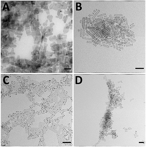
Figure 1. TEM images of (A) CdS NPLs, (B) CdS–Au, (C) CdS–Pt, and (D) CdS–PtNi HNSs. All scale bars are 50 nm.
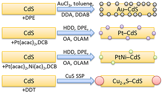
Scheme 1. General schematics of the synthetic methods used to grow the different described metal and Cu2−xS domains on CdS NPLs.
The XRD pattern of as-synthesized CdS shown in Figure 2A is slightly shifted to higher 2 theta values compared to the literature values of bulk, hexagonal CdS (JCPDS No. 41-1049) and agrees with the result published previously for such NPLs (Son et al., 2012). After the growth of Au on the NPLs, an additional weak diffraction is present around 38°, which corresponds to the (111) plane of cubic Au (JCPDS No. 04-0784). The presence of the cubic Au phase was further verified by FFT analysis, calculated from high-resolution TEM (HRTEM) images, with experimental d111 = 2.344 Å (Supplementary Figure 2). The XRD patterns of CdS–Pt and CdS–PtNi both have two additional peaks compared to pristine CdS. These peaks correspond to the literature values of fcc Pt diffractions around 40° and 46° (JCPDS No. 04-0802). However, the diffractions attributed to Pt in the CdS–PtNi alloy HNS are shifted compared to the CdS–Pt by 0.8°. Assuming Vegard's law validity and that both Pt and Ni are in their fcc crystal structure (dPt, 111 = 2.265 Å, dNi, 111 = 2.034 Å, JCPDS No. 04-0850), the alloy's calculated composition corresponds to an atomic Pt:Ni ratio of about 4.3:1.
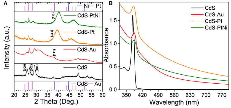
Figure 2. (A) XRD patterns and (B) UV-vis spectra of pristine CdS NPLs and CdS–M HNSs. JCPDS numbers of CdS, Au, Pt, and Ni literature patterns in panel A are 41-1049, 04-0784, 04-0802, and 04-0850, respectively. The broad peak around 30° in the CdS–Au diffraction pattern may be attributed to the presence of surfactants.
To confirm the presence of Au, Pt, and Ni in all M–SC HNS samples, EDS data was collected from a large quantity of the hybrid structures using an SEM instrument (Supplementary Figure 3). For the CdS–Au sample, the atomic ratio of Au:Cd:S was 1.8:1:3.5. The high S content compared to Cd may be due to partial overlap between the S-K and Au-M transitions at 2.3 and 2.1 kV, respectively. To minimize the quantitative error, the gold's L edge was used for the atomic ratio calculation, and yet the overlap is probably responsible for the overestimated S-to-Cd ratio. The atomic ratio of Pt:Cd:S in the CdS–Pt sample was 1.3:1:1.8, and the atomic ratio of Pt:Ni:Cd:S in the CdS–PtNi sample was 1.1:0.26:1:1.6. Again, the high S amount compared to Cd in both samples may stem from partial overlap between the strong S-K and Pt-M transitions at 2.3 and 2.05 kV, respectively, hence for the quantitative calculation Pt-L was used. From this EDS result, we may calculate an atomic ratio of Pt:Ni of 4.2:1 for the CdS–PtNi sample. This ratio agrees with the calculated ratio based on the shift of the PtNi (111) diffraction relative to the one of Pt in the XRD. The atomic ratio of Pt:Ni was further verified with EDS using a TEM instrument (Supplementary Figure 4), providing a ratio 3.3:1 between the two, and Pt:Ni:Cd:S atomic ratio of 1.4:0.42:1:1.3. Notably, both XRD and EDS data indicate that the Ni content in the NiPt product is lower than in the reacting precursors. This result most probably stems from the higher reactivity of Pt compared to Ni toward nucleation on the thin CdS NPLs. As was shown in the past by our group, the mechanism of PtCo alloy tips formation on CdS nanorods, involves first the nucleation of Pt, which is then alloyed with the other metal (Yuhas et al., 2009). When the final metal particle size is smaller than 7.2 nm, the relative alloying metal amount is low (3:1 Pt:Co for 3.6 ± 1.1 PtCo tips), and a 1:1 ratio can only be achieved for larger NPs (Habas et al., 2008; Yuhas et al., 2009). In the PtNi alloy tips, an average 25% Ni relative to Pt was measured for a diameter of 4.7 nm (Habas et al., 2008), which agrees with the findings from XRD and SEM-EDS for CdS NPL–NiPt HNS.
The UV-vis absorption of as-synthesized CdS together with the M–SC samples is presented in Figure 2B. All M–SC samples have increased absorbance in the visible region compared to CdS, in agreement with previously-published CdS–Pt and CdSe/CdS–Au systems (Chauhan et al., 2016; Li et al., 2018). The absence of a peak at the position of the Au plasmon in the CdS–Au sample also agrees with previously published data and is attributed to the small size of the decorating Au particles.
For the formation of SC–SC HNS, copper sulfide was chosen because the stoichiometric composition of Cu-S compounds can vary from copper-rich chalcocite (Cu2S) to copper-poor villamaninite (CuS2), which endows their variable electronic properties. For example, Cu2S–CdS HNS is considered a candidate material for applications requiring solar light harvesting as photovoltaic devices (Pan et al., 2012; Wong et al., 2015) since it combines the formation of a favorable band alignment (staggered type II band positions), which facilitates charge separation across the p-Cu2S–n-CdS SC–SC interface and two distinct optical band gaps, which increase light absorbance in different parts of the solar spectrum (Rivest et al., 2011; Jen-La Plante et al., 2014). As the synthetic route, we have chosen to work with single-source molecular precursors. Specifically, we demonstrate a Cu2−xS–CdS NPLs hybrid system in Figure 3A. The benefit of the SSP is the presence of both elemental ingredients of the final SC in stoichiometric ratios in the precursor (Volokh et al., 2018). Since there is no difference in the reactivity of the S-source and the Cu-source, we had expected the CdS in this synthetic path to be less prone to partial cationic exchange of the cadmium with copper. The result is decoration of the “tips” of the 2D CdS NPLs with copper sulfide NPs.
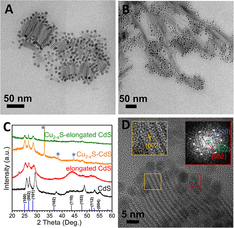
Figure 3. Growth of Cu2−xS on CdS NPLs. TEM images of (A) Cu2−xS–CdS NPLs and (B) Cu2−xS–elongated CdS NPLs, (C) XRD patterns, and (D) HRTEM image of Cu2−xS–CdS NPLs. The sharp peaks marked by asterisks in (C) originate from the substrate. The left inset in (D) is an enlargement of the area marked in yellow with hexagonal CdS (002) plane labeling. Right inset is an FFT analysis of the area marked in red of Cu2−xS, corresponding to a hexagonal symmetry, and (100), (002), and (102) planes of high chalcocite Cu2S.
The Cu2−xS NPs (d = 7.1 ± 0.8 nm, Supplementary Figure 5A) can be clearly seen at the tips of the CdS NPLs in the TEM images. Moreover, to demonstrate the scalability of this synthesis, we have used elongated CdS NPLs (which have a length of about 50–200 nm and a thickness of ~1 nm, Supplementary Figure 6) as the substrates for the growth of similar Cu2−xS NPs. Similarly, Cu2−xS NPs (d = 6.4 ± 1.0 nm, Supplementary Figure 5B) also grow successfully at the tips of the elongated CdS NPLs (Figure 3B). XRD of this hybrid system in Figure 3C shows the clear diffraction pattern of hexagonal CdS (wurtzite CdS, JCPDS No. 41-1049). Unfortunately, it is impossible to distinguish the diffraction of the copper sulfide (possibly, due to its small size and relative low amount) from the CdS diffraction at the same position. As the accuracy of EDS analysis for a colloidal copper sulfide system is limited due to one or more of the following: multiple Cu2−xS phases with x < 1, variable vacancies amount, partial surface oxidation, and possible elements detection due to remaining reaction byproducts and the use of DDT as the ligand, the EDS spectrum (Supplementary Figure 7) was used to qualitatively confirm the presence of Cu, Cd, and S in the product. The UV-vis absorption spectra are presented in Supplementary Figure 8. A main absorption peak at 378 nm along with a shoulder at 383 nm appeared in CdS NPLs, which originate from the electron-light hole and electron-heavy hole transitions, respectively, and indicate CdS thickness of about 5 molecular layers (Ithurria et al., 2011b). In the case of elongated 2D CdS NPLs, another peak at 414 nm was found. After deposition of Cu2−xS, in both cases, the CdS NPLs' peaks were blue-shifted and lowered in their relative intensity. Furthermore, a new peak around 500 nm appears in the hybrid system. Absorption about this wavelength was reported for hexagonal Cu2S (Mondal et al., 2014) and for several Cu2−xS phases such as Cu1.8S, Cu1.97S (Zhao et al., 2009), and Cu7S4 (Jiang et al., 2000; Behboudnia and Khanbabaee, 2007). From HRTEM image analysis (Figure 3D), the growth of the copper sulfide domain at the tips of the elongated CdS structure is evident. FFT analyses of the Cu2−xS NPs over the area indicated by the red square in Figure 3D show the crystal planes with distances of 0.3493, 0.3277, and 0.2469 nm. These lattice spacings and angles in the FFT correspond to the (100), (002), and (102) planes of hexagonal Cu2S [high chalcocite Cu2S, Pearson's crystal data, entry no. 1003706 (Will et al., 2002)], respectively. Additional analysis of other HNSs gives the same result, and an example HRTEM image is presented in Supplementary Figure 9. Moreover, the lattice distances of 15 different Cu2−xS NPs (Supplementary Figure 10) were measured, all of which are consistent with the above hexagonal Cu2S with mismatches <3% (Supplementary Table 1). Though it is challenging to unequivocally determine the crystal structure because the XRD diffractions of Cu2−xS are not obvious and several different Cu2−xS phases have lattice spacings close to our experimental measured values, the most probable phase is the hexagonal Cu2S as discussed above, and it matches with reported optical activity. In the case of the CdS NPL part of the hybrid, the measured plane seen in the yellow square of Figure 3D, has an experimental spacing of about 0.337 nm, which suits the (002) of hexagonal CdS, also present in the XRD. To check the stability of the Cu2−xS–CdS HNS, we have also measured the XRD of a sample 2 months after synthesis and no evident diffraction changes were seen (Supplementary Figure 11). Apart from stability, this measurement indicates that no significant cation exchange-induced phenomenon exists in the Cu2−xS–CdS hybrid, as copper can easily diffuse in the CdS lattice even at room temperature in nanostructures (Rivest et al., 2011).
Conclusions and Summary
In summary, we have developed a facile and scalable colloidal synthetic strategy to selectively grow metal (Au, Pt, PtNi alloy) and semiconductor (Cu2−xS, probably Cu2S) domains on CdS nanoplates. With significant similarity to CdS nanorods, metal reduction on high-energy locations of a nanostructured template results in the formation of metal–CdS heterostructure(s). The use of single-source molecular precursors allowed formation of SC–SC hybrid of two metal sulfides, where the CdS nanoplate remains relatively intact without significant cation exchange phenomena occurring, and Cu2−xS nanoparticles decorate its edges forming multiple interfaces. Due to the generality of this approach, other metals (and their alloys) as well as other semiconductor as metal sulfides can be prepared via this approach.
Data Availability Statement
All datasets generated for this study are included in the article/Supplementary Material.
Author Contributions
All authors contributed to the analysis, writing of the manuscript, and approved its final form.
Conflict of Interest
The authors declare that the research was conducted in the absence of any commercial or financial relationships that could be construed as a potential conflict of interest.
Acknowledgments
The authors thank the IKI electron microscopy unit staff: Dr. Volodia Ezersky for expert aid with analytical TEM and fruitful discussion and Dr. Alexander Upcher for HRTEM measurements. HF thanks the Arianne de Rothschild scholarship program for female Ph.D. students from the Rothschild Caesarea Foundation and the Chemo-Tech scholarship from the Ben-Gurion University of the Negev for financial support; LT thanks the Negev fellowship for financial support.
Supplementary Material
The Supplementary Material for this article can be found online at: https://www.frontiersin.org/article/10.3389/fmats.2019.00345/full#supplementary-material
References
Akkerman, Q. A., Martín-García, B., Buha, J., Almeida, G., Toso, S., Marras, S., et al. (2019). Ultrathin orthorhombic PbS nanosheets. Chem. Mater. 31, 8145–8153. doi: 10.1021/acs.chemmater.9b02914
Banin, U., Ben-Shahar, Y., and Vinokurov, K. (2014). Hybrid semiconductor–metal nanoparticles: from architecture to function. Chem. Mater. 26, 97–110. doi: 10.1021/cm402131n
Behboudnia, M., and Khanbabaee, B. (2007). Investigation of nanocrystalline copper sulfide Cu7S4 fabricated by ultrasonic radiation technique. J. Cryst. Growth 304, 158–162. doi: 10.1016/j.jcrysgro.2007.02.016
Berends, A. C., van der Stam, W., Akkerman, Q. A., Meeldijk, J. D., van der Lit, J., and de Mello Donega, C. (2018). Anisotropic 2D Cu2-xSe nanocrystals from dodecaneselenol and their conversion to CdSe and CuInSe2 nanoparticles. Chem. Mater. 30, 3836–3846. doi: 10.1021/acs.chemmater.8b01143
Brovelli, S., Schaller, R. D., Crooker, S. A., García-Santamaría, F., Chen, Y., Viswanatha, R., et al. (2011). Nano-engineered electron-hole exchange interaction controls exciton dynamics in core-shell semiconductor nanocrystals. Nat. Commun. 2:280. doi: 10.1038/ncomms1281
Carbone, L., and Cozzoli, P. D. (2010). Colloidal heterostructured nanocrystals: synthesis and growth mechanisms. Nano Today 5, 449–493. doi: 10.1016/j.nantod.2010.08.006
Carey, G. H., Abdelhady, A. L., Ning, Z., Thon, S. M., Bakr, O. M., and Sargent, E. H. (2015). Colloidal quantum dot solar cells. Chem. Rev. 115, 12732–12763. doi: 10.1021/acs.chemrev.5b00063
Chang, Y., Yu, K., Zhang, C., Yang, Z., Feng, Y., Hao, H., et al. (2017). Ternary CdS/Au/3DOM-SrTiO3 composites with synergistic enhancement for hydrogen production from visible-light photocatalytic water splitting. Appl. Catal. B Environ. 215, 74–84. doi: 10.1016/j.apcatb.2017.05.054
Chauhan, H., Kumar, Y., Dana, J., Satpati, B., Ghosh, H. N., and Deka, S. (2016). Photoinduced ultrafast charge separation in colloidal 2-dimensional CdSe/CdS-Au hybrid nanoplatelets and corresponding application in photocatalysis. Nanoscale 8, 15802–15812. doi: 10.1039/c6nr03610d
Cho, Y., Pak, S., An, G., Hou, B., and Cha, S. (2019). Quantum dots for hybrid energy harvesting: from integration to piezo-phototronics. Isr. J. Chem. 59, 747–761. doi: 10.1002/ijch.201900035
Chu, J., Han, X., Yu, Z., Du, Y., Song, B., and Xu, P. (2017). Fabrication of H-TiO2/CdS/Cu2-xS ternary heterostructures for enhanced photocatalytic hydrogen production. Chem. Select 2, 2681–2686. doi: 10.1002/slct.201700419
Costi, R., Saunders, A. E., and Banin, U. (2010). Colloidal hybrid nanostructures: a new type of functional materials. Angew. Chemie Int. Ed. 49, 4878–4897. doi: 10.1002/anie.200906010
Cozzoli, P. D., Pellegrino, T., and Manna, L. (2006). Synthesis, properties and perspectives of hybrid nanocrystal structures. Chem. Soc. Rev. 35, 1195. doi: 10.1039/b517790c
Cui, C., Gan, L., Li, H.-H., Yu, S.-H., Heggen, M., and Strasser, P. (2012). Octahedral PtNi nanoparticle catalysts: exceptional oxygen reduction activity by tuning the alloy particle surface composition. Nano Lett. 12, 5885–5889. doi: 10.1021/nl3032795
Das, S., Satpati, B., Chauhan, H., Deka, S., Ghosalya, M. K., Gopinath, C. S., et al. (2016). Seeding of Au on CdSe/CdS nanoplates using Langmuir-Blodgett technique. RSC Adv. 6, 14658–14665. doi: 10.1039/c5ra26018c
Davis, A. H., Hofman, E., Chen, K., Li, Z. J., Khammang, A., Zamani, H., et al. (2019). Exciton energy shifts and tunable dopant emission in manganese-doped two-dimensional CdS/ZnS core/shell nanoplatelets. Chem. Mater. 31, 2516–2523. doi: 10.1021/acs.chemmater.9b00006
Dufour, M., Izquierdo, E., Livache, C., Martinez, B., Silly, M. G., Pons, T., et al. (2019). Doping as a strategy to tune color of 2D colloidal nanoplatelets. ACS Appl. Mater. Interfaces 11, 10128–10134. doi: 10.1021/acsami.8b18650
Feng, F., Nguyen, L. T., Nasilowski, M., Nadal, B., Dubertret, B., Coolen, L., et al. (2018). Consequence of shape elongation on emission asymmetry for colloidal CdSe/CdS nanoplatelets. Nano Res. 11, 3593–3602. doi: 10.1007/s12274-017-1926-3
Flomin, K., Diab, M., and Mokari, T. (2017). Ternary hybrid nanostructures of Au–CdS–ZnO grown via a solution–liquid–solid route using Au–ZnO catalysts. Nanoscale 9, 16138–16142. doi: 10.1039/C7NR06382B
Ganguly, P., Harb, M., Cao, Z., Cavallo, L., Breen, A., Dervin, S., et al. (2019). 2D nanomaterials for photocatalytic hydrogen production. ACS Energy Lett. 4, 1687–1709. doi: 10.1021/acsenergylett.9b00940
Habas, S. E., Yang, P., and Mokari, T. (2008). Selective growth of metal and binary metal tips on CdS nanorods. J. Am. Chem. Soc. 130, 3294–3295. doi: 10.1021/ja800104w
Ithurria, S., Bousquet, G., and Dubertret, B. (2011a). Continuous transition from 3D to 1D confinement observed during the formation of CdSe nanoplatelets. J. Am. Chem. Soc. 133, 3070–3077. doi: 10.1021/ja110046d
Ithurria, S., Tessier, M. D., Mahler, B., Lobo, R. P. S. M., Dubertret, B., and Efros, A. L. (2011b). Colloidal nanoplatelets with two-dimensional electronic structure. Nat. Mater. 10, 936–941. doi: 10.1038/nmat3145
Jen-La Plante, I., Teitelboim, A., Pinkas, I., Oron, D., and Mokari, T. (2014). Exciton quenching due to copper diffusion limits the photocatalytic activity of CdS/Cu2S nanorod heterostructures. J. Phys. Chem. Lett. 5, 590–596. doi: 10.1021/jz500041g
Jen-La Plante, I., Zeid, T. W., Yang, P., and Mokari, T. (2010). Synthesis of metal sulfide nanomaterials via thermal decomposition of single-source precursors. J. Mater. Chem. 20, 6612–6617. doi: 10.1039/c0jm00439a
Jiang, X., Xie, Y., Lu, J., He, W., Zhu, L., and Qian, Y. (2000). Preparation and phase transformation of nanocrystalline copper sulfides (Cu9S8, Cu7S4 and CuS) at low temperature. J. Mater. Chem. 10, 2193–2196. doi: 10.1039/b002486o
Kaltwasser, M., Schmidt, U., Biswas, S., Reiprich, J., Schlag, L., Isaac, N. A., et al. (2018). Core–shell transformation-imprinted solder bumps enabling low-temperature fluidic self-assembly and self-alignment of chips and high melting point interconnects. ACS Appl. Mater. Interfaces 10, 40608–40613. doi: 10.1021/acsami.8b12390
Kelestemur, Y., Dede, D., Gungor, K., Usanmaz, C. F., Erdem, O., and Demir, H. V. (2017). Alloyed heterostructures of CdSexS1−xnanoplatelets with highly tunable optical gain performance. Chem. Mater. 29, 4857–4865. doi: 10.1021/acs.chemmater.7b00829
Khan, M. R., Chuan, T. W., Yousuf, A., Chowdhury, M. N. K., and Cheng, C. K. (2015). Schottky barrier and surface plasmonic resonance phenomena towards the photocatalytic reaction: study of their mechanisms to enhance photocatalytic activity. Catal. Sci. Technol. 5, 2522–2531. doi: 10.1039/C4CY01545B
Kim, Y., Park, K. Y., Jang, D. M., Song, Y. M., Kim, H. S., Cho, Y. J., et al. (2010). Synthesis of Au–Cu2S core–shell nanocrystals and their photocatalytic and electrocatalytic activity. J. Phys. Chem. C 114, 22141–22146. doi: 10.1021/jp109127m
Kormilina, T. K., Cherevkov, S. A., Fedorov, A. V., and Baranov, A. V. (2017). Cadmium chalcogenide nano-heteroplatelets: creating advanced nanostructured materials by shell growth, substitution, and attachment. Small 13:1702300. doi: 10.1002/smll.201702300
Kovalenko, M. V, Manna, L., Cabot, A., Hens, Z., Talapin, D. V, Kagan, C. R., et al. (2015). Prospects of nanoscience with nanocrystals. ACS Nano 9, 1012–1057. doi: 10.1021/nn506223h
Kudera, S., Carbone, L., Casula, M. F., Cingolani, R., Falqui, A., Snoeck, E., et al. (2005). Selective growth of PbSe on one or both tips of colloidal semiconductor nanorods. Nano Lett. 5, 445–449. doi: 10.1021/nl048060g
Lee, Y. K., Jung, C. H., Park, J., Seo, H., Somorjai, G. A., and Park, J. Y. (2011). Surface plasmon-driven hot electron flow probed with metal-semiconductor nanodiodes. Nano Lett. 11, 4251–4255. doi: 10.1021/nl2022459
Li, M., Chen, J.-S., and Cotlet, M. (2019). Light-induced interfacial phenomena in atomically thin 2D van der Waals material hybrids and heterojunctions. ACS Energy Lett. 4, 2323–2335. doi: 10.1021/acsenergylett.9b01399
Li, Q., and Lian, T. (2018). Exciton dissociation dynamics and light-driven H2 generation in colloidal 2D cadmium chalcogenide nanoplatelet heterostructures. Nano Res. 11, 3031–3049. doi: 10.1007/s12274-018-2024-x
Li, Q., Wu, K., Chen, J., Chen, Z., McBride, J. R., and Lian, T. (2016). Size-independent exciton localization efficiency in colloidal CdSe/CdS Core/Crown nanosheet type-I heterostructures. ACS Nano 10, 3843–3851. doi: 10.1021/acsnano.6b00787
Li, Q., Zhao, F., Qu, C., Shang, Q., Xu, Z., Yu, L., et al. (2018). Two-dimensional morphology enhances light-driven H2 generation efficiency in CdS nanoplatelet-Pt heterostructures. J. Am. Chem. Soc. 140, 11726–11734. doi: 10.1021/jacs.8b06100
Liu, R., Duay, J., and Lee, S. B. (2010). Redox exchange induced MnO2 nanoparticle enrichment in poly(3,4-ethylenedioxythiophene) nanowires for electrochemical energy storage. ACS Nano 4, 4299–4307. doi: 10.1021/nn1010182
Liu, Y., Yin, D., and Swihart, M. T. (2018). Ag + -induced shape and composition evolution of covellite CuS nanoplatelets to produce plate–satellite and biconcave–particle heterostructures. Chem. Mater. 30, 8089–8098. doi: 10.1021/acs.chemmater.8b04272
Loukrakpam, R., Luo, J., He, T., Chen, Y., Xu, Z., Njoki, P. N., et al. (2011). Nanoengineered PtCo and PtNi catalysts for oxygen reduction reaction: an assessment of the structural and electrocatalytic properties. J. Phys. Chem. C 115, 1682–1694. doi: 10.1021/jp109630n
Ma, S., Deng, Y., Xie, J., He, K., Liu, W., Chen, X., et al. (2018). Noble-metal-free Ni3C cocatalysts decorated CdS nanosheets for high-efficiency visible-light-driven photocatalytic H2 evolution. Appl. Catal. B Environ. 227, 218–228. doi: 10.1016/j.apcatb.2018.01.031
Ma, S., Xie, J., Wen, J., He, K., Li, X., Liu, W., et al. (2017). Constructing 2D layered hybrid CdS nanosheets/MoS2 heterojunctions for enhanced visible-light photocatalytic H2 generation. Appl. Surf. Sci. 391, 580–591. doi: 10.1016/j.apsusc.2016.07.067
Mahler, B., Guillemot, L., Bossard-Giannesini, L., Ithurria, S., Pierucci, D., Ouerghi, A., et al. (2016). Metallic functionalization of CdSe 2D nanoplatelets and its impact on electronic transport. J. Phys. Chem. C 120, 12351–12361. doi: 10.1021/acs.jpcc.6b02101
Marcovici, A., Le Saux, G., Bhingardive, V., Rukenstein, P., Flomin, K., Shreteh, K., et al. (2018). Directed assembly of Au-tipped 1D inorganic nanostructures via nanolithographic docking. ACS Nano 12, 10016–10023. doi: 10.1021/acsnano.8b04443
Maynadiø, J., Salant, A., Falqui, A., Respaud, M., Shaviv, E., Banin, U., et al. (2009). Cobalt growth on the tips of CdSe Nanorods. 1814–1817. doi: 10.1002/anie.200804798
Milliron, D., Hughes, S. M., Cui, Y., Manna, L., Li, J., Wang, L. W., et al. (2004). Colloidal nanocrystal heterostructures with linear and branched topology. Nature 430, 190–195. doi: 10.1038/nature02695
Min, Y., Im, E., Hwang, G.-T. T., Kim, J.-W. W., Ahn, C.-W. W., Choi, J.-J., et al. (2019). Heterostructures in two-dimensional colloidal metal chalcogenides: synthetic fundamentals and applications. Nano Res. 12, 1750–1769. doi: 10.1007/s12274-019-2432-6
Mirkovic, T., Rossouw, D., Botton, G. A., and Scholes, G. D. (2011). Broken band alignment in EuS-CdS nanoheterostructures. Chem. Mater. 23, 181–187. doi: 10.1021/cm102565y
Mishra, N., Lian, J., Chakrabortty, S., Lin, M., and Chan, Y. (2012). Unusual selectivity of metal deposition on tapered semiconductor nanostructures. Chem. Mater. 24, 2040–2046. doi: 10.1021/cm300161m
Mokari, T., Sztrum, C. G., Salant, A., Rabani, E., and Banin, U. (2005). Formation of asymmetric one-sided metal-tipped semiconductor nanocrystal dots and rods. Nat. Mater. 4, 855–863. doi: 10.1038/nmat1505
Mondal, G., Santra, A., Jana, S., Mandal, T. N., Mondal, A., and Seok, S., Il, et al. (2014). Precursor-driven selective synthesis of hexagonal chalcocite (Cu2S) nanocrystals: structural, optical, electrical and photocatalytic properties. New J. Chem. 38, 4774–4782. doi: 10.1039/c4nj00584h
Nasilowski, M., Mahler, B., Lhuillier, E., Ithurria, S., and Dubertret, B. (2016). Two-dimensional colloidal nanocrystals. Chem. Rev. 116, 10934–10982. doi: 10.1021/acs.chemrev.6b00164
Naskar, S., Lübkemann, F., Hamid, S., Freytag, A., Wolf, A., Koch, J., et al. (2017). Synthesis of ternary and quaternary Au and Pt decorated CdSe/CdS heteronanoplatelets with controllable morphology. Adv. Funct. Mater. 27:1604685. doi: 10.1002/adfm.201604685
Pan, C., Niu, S., Ding, Y., Dong, L., Yu, R., Liu, Y., et al. (2012). Enhanced Cu2S/CdS coaxial nanowire solar cells by piezo-phototronic effect. Nano Lett. 12, 3302–3307. doi: 10.1021/nl3014082
Paulus, U. A., Wokaun, A., Scherer, G. G., Schmidt, T. J., Stamenkovic, V., Radmilovic, V., et al. (2002). Oxygen reduction on carbon-supported Pt–Ni and Pt–Co alloy catalysts. J. Phys. Chem. B 106, 4181–4191. doi: 10.1021/jp013442l
Riedinger, A., Ott, F. D., Mule, A., Mazzotti, S., Knüsel, P. N., Kress, S. J. P., et al. (2017). An intrinsic growth instability in isotropic materials leads to quasi-two-dimensional nanoplatelets. Nat. Mater. 16, 743–748. doi: 10.1038/nmat4889
Rivest, J. B., Swisher, S. L., Fong, L. K., Zheng, H., and Paul Alivisatos, A. (2011). Assembled monolayer nanorod heterojunctions. ACS Nano 5, 3811–3816. doi: 10.1021/nn2001454
Rukenstein, P., Jen-La Plante, I., Diab, M., Chockler, E., Flomin, K., Moshofsky, B., et al. (2012). Selective growth of metal sulfide tips onto cadmium chalcogenide nanostructures. CrystEngComm 14:7590. doi: 10.1039/c2ce25795e
Saidzhonov, B. M., Kozlovsky, V. F., Zaytsev, V. B., and Vasiliev, R. B. (2019). Ultrathin CdSe/CdS and CdSe/ZnS core-shell nanoplatelets: the impact of the shell material on the structure and optical properties. J. Lumin. 209, 170–178. doi: 10.1016/j.jlumin.2019.01.052
Shaviv, E., and Banin, U. (2010). Synergistic effects on second harmonic generation of hybrid CdSe–Au nanoparticles. ACS Nano 4, 1529–1538. doi: 10.1021/nn901778k
Son, J. S., Park, K., Kwon, S. G., Yang, J., Choi, M. K., Kim, J., et al. (2012). Dimension-controlled synthesis of CdS nanocrystals: from 0D quantum dots to 2D nanoplates. Small 8, 2394–2402. doi: 10.1002/smll.201200506
Tan, C., Chen, J., Wu, X.-J., and Zhang, H. (2018). Epitaxial growth of hybrid nanostructures. Nat. Rev. Mater. 3:17089. doi: 10.1038/natrevmats.2017.89
Tongying, P., Plashnitsa, V. V., Petchsang, N., Vietmeyer, F., Ferraudi, G. J., Krylova, G., et al. (2012). Photocatalytic hydrogen generation efficiencies in one-dimensional CdSe heterostructures. J. Phys. Chem. Lett. 3, 3234–3240. doi: 10.1021/jz301628b
Urban, J. J., Talapin, D. V, Shevchenko, E. V, Kagan, C. R., and Murray, C. B. (2007). Synergism in binary nanocrystal superlattices leads to enhanced p-type conductivity in self-assembled PbTe/Ag2Te thin films. Nat. Mater. 6, 115–121. doi: 10.1038/nmat1826
Volokh, M., Diab, M., Flomin, K., and Mokari, T. (2018). Electrophoretic deposition of single-source precursors as a general approach for the formation of hybrid nanorod array heterostructures. J. Colloid Interface Sci. 515, 221–231. doi: 10.1016/j.jcis.2018.01.030
Volokh, M., Diab, M., Magen, O., Jen-La Plante, I., Flomin, K., Rukenstein, P., et al. (2014). Coating and enhanced photocurrent of vertically aligned zinc oxide nanowire arrays with metal sulfide materials. ACS Appl. Mater. Interfaces 6, 13594–13599. doi: 10.1021/am502976v
Volokh, M., Peng, G., Barrio, J., and Shalom, M. (2019). Carbon nitride materials for water splitting photoelectrochemical cells. Angew. Chemie Int. Ed. 58, 6138–6151. doi: 10.1002/anie.201806514
Waiskopf, N., Ben-Shahar, Y., and Banin, U. (2018). Photocatalytic hybrid semiconductor-metal nanoparticles; from synergistic properties to emerging applications. Adv. Mater. 30:1706697. doi: 10.1002/adma.201706697
Wang, Y., Zhukovskyi, M., Tongying, P., Tian, Y., and Kuno, M. (2014). Synthesis of ultrathin and thickness-controlled Cu2-xSe nanosheets via cation exchange. J. Phys. Chem. Lett. 5, 3608–3613. doi: 10.1021/jz5019288
Will, G., Hinze, E., and Abdelrahman, A. R. M. (2002). Crystal structure analysis and refinement of digenite, Cu1.8S, in the temperature range 20 to 500 C under controlled sulfur partial pressure. Eur. J. Mineral. 14, 591–598. doi: 10.1127/0935-1221/2002/0014-0591
Wong, A. B., Brittman, S., Yu, Y., Dasgupta, N. P., and Yang, P. (2015). Core–Shell CdS–Cu2S nanorod array solar cells. Nano Lett. 15, 4096–4101. doi: 10.1021/acs.nanolett.5b01203
Yu, Z., Quo, L., Du, H., Krauss, T., and Silcox, J. (2005). Shell distribution on colloidal CdSe/ZnS quantum dots. Nano Lett. 5, 565–570. doi: 10.1021/nl048245n
Yuhas, B. D., Habas, S. E., Fakra, S. C., and Mokari, T. (2009). Probing compositional variation within hybrid nanostructures. ACS Nano 3, 3369–3376. doi: 10.1021/nn901107p
Zhang, H., Savitzky, B. H., Yang, J., Newman, J. T., Perez, K. A., Hyun, B. R., et al. (2016). Colloidal synthesis of PbS and PbS/CdS nanosheets using acetate-free precursors. Chem. Mater. 28, 127–134. doi: 10.1021/acs.chemmater.5b03348
Zhang, L., Jean, S. R., Li, X., Sack, T., Wang, Z., Ahmed, S., et al. (2018). Programmable metal/semiconductor nanostructures for mRNA-modulated molecular delivery. Nano Lett. 18, 6222–6228. doi: 10.1021/acs.nanolett.8b02263
Zhao, Y., Pan, H., Lou, Y., Qiu, X., Zhu, J., and Burda, C. (2009). Plasmonic Cu2-xS nanocrystals: optical and structural properties of copper-deficient copper(I) sulfides. J. Am. Chem. Soc. 131, 4253–4261. doi: 10.1021/ja805655b
Zhi, L., Hu, Y., El Hamaoui, B., Wang, X., Lieberwirth, I., Kolb, U., et al. (2008). Precursor-controlled formation of novel carbon/metal and carbon/metal oxide nanocomposites. Adv. Mater. 20, 1727–1731. doi: 10.1002/adma.200702654
Keywords: hybrid nanoparticle, hybrid nanostructure, semiconductor–semiconductor, semiconductor–metal, two-dimensional CdS, nanoplate, interface
Citation: Fridman H, Tian L, Shreteh K, Volokh M and Mokari T (2020) Selective Growth of Metal Sulfide, Metal, and Metal-Alloy on 2D CdS Nanoplates. Front. Mater. 6:345. doi: 10.3389/fmats.2019.00345
Received: 06 October 2019; Accepted: 18 December 2019;
Published: 15 January 2020.
Edited by:
P. Davide Cozzoli, University of Salento, ItalyReviewed by:
Katerina Soulantica, UMR5215 Laboratoire de Physique et Chimie des Nano-Objets (LPCNO), FranceNarayan Pradhan, Indian Association for the Cultivation of Science, India
Marianna Casavola, University of Southampton, United Kingdom
Kwangyeol Lee, Korea University, South Korea
Copyright © 2020 Fridman, Tian, Shreteh, Volokh and Mokari. This is an open-access article distributed under the terms of the Creative Commons Attribution License (CC BY). The use, distribution or reproduction in other forums is permitted, provided the original author(s) and the copyright owner(s) are credited and that the original publication in this journal is cited, in accordance with accepted academic practice. No use, distribution or reproduction is permitted which does not comply with these terms.
*Correspondence: Taleb Mokari, bW9rYXJpQGJndS5hYy5pbA==
†These authors have contributed equally to this work