 Xueli Shen1
 Yandong Wang1Jianping Li1Yangkai Chen1Zhifang Wang2
 Wenchong Wang2*
 Lizhen Huang1*Lifeng Chi1*
- 1Jiangsu Key Laboratory for Carbon-Based Functional Materials & Devices, Institute of Functional Nano & Soft Materials, Joint International Research Laboratory of Carbon-Based Functional Materials and Devices, Soochow University, Suzhou, China
- 2Physikalisches Institut and Center for Nanotechnology, Universität Münster, Münster, Germany
A vacuum evaporator is widely used for generating atomic/molecular beams for thin film deposition, and conventionally must be mounted to a vacuum chamber with an upwards angle from the horizontal. In this article, we report a novel kind of evaporator that can be mounted at an arbitrary angle for organic materials. The crucible of the evaporator here is designed to keep the loaded organic materials from falling. The morphology and electrical characteristics of pentacene thin film organic field effect transistors on trichloro(octadecyl)silane modified SiO2 are characterized and compared for commercial and arbitrary mounting angle evaporators. Pentacene films deposited from both evaporators exhibit similar morphology and domain size characterized by atomic force microscope, as well as similar mobility, threshold voltage, and on/off ratio. The results can be used to develop a new configuration for an organic vacuum deposition system, which allows the positioning of shadow masks directly on substrates and thus avoids deformation, enabling fabrication of organic electronics for high resolution over large areas.
Introduction
Small molecule organic semiconductors have attracted much attention owing to their extensive applications in organic electronics and opto-electronics such as organic light emitting diodes (OLEDs), organic field effect transistors (OFETs), and organic photovoltaics (OPVs; Forrest, 2004; Dong et al., 2013). Since the reports of thin film organic electronic and opto-electronic devices in the 1980s, there has been exciting progress in material synthesis, film preparation, and device construction and processing (Tsumura et al., 1986; Tang and VanSlyke, 1987; Kelley et al., 2004; Kan et al., 2018). Typically, organic semiconductor devices are built on one or several thin functional layers fabricated by various techniques e.g., vacuum deposition and solution processable techniques such as spin-coating and ink-jet printing (Yuan et al., 2014; Matsui et al., 2019; Li et al., 2020). Vacuum deposition is one of the mainstream film preparation techniques for small molecular organic semiconductors because it provides high purity, precise layer thickness control, interface engineering, and uniformity over large areas. The vacuum deposition system consists of vacuum chambers with vacuum pumps and gauges, sample holders with heating and/or cooling elements for sample temperature control, evaporators for thin film deposition, and quartz balances for in situ thickness monitoring. The materials to be deposited are loaded into crucibles and require a low vapor pressure under vacuum conditions. Conventionally, the crucibles are bowl or tube shaped, with one closed end and another open end for the outlet of molecule vapor. Normally, the evaporators have to be mounted to the vacuum chamber with the opening facing upwards, to prevent the loaded materials from falling (Quiroga et al., 2011).
For organic electronic devices, such OFETs and OLEDs, patterning of thin functional layers such as active layers and electrodes are required for device arrays and integration (Ling and Bao, 2004; Zhu et al., 2019). Although various patterning techniques have been developed, fine metal mask (FMM) is still a widely used method, owing to its established procedure and high reliability (Kim et al., 2020). For the vacuum deposition system with conventional evaporators, samples are placed over the evaporators with FMM in-between, which presents challenges like deformation of FMM induced by gravity and hinders further applications in high resolution and large area patterning. An evaporator that could be mounted above the sample holder is much needed, as it would enable the FMM to be supported by the sample and avoids its deformation. In addition, for specific applications such as in situ analysis, the evaporator and analytic units have to be installed on the same side for real time measurements (Annese et al., 2018). Owing to the limited space in the bottom of the vacuum chamber, it would be beneficial to have an arbitrary mounting angle evaporator (AMAE), installed according to the position of analytic units.
In this article, we report on an evaporator for organic compounds, with a crucible designed to keep the loaded materials from falling at any mounting angle. The evaporator is further mounted in the top space of a high vacuum chamber and demonstrated using a classic p-type small molecular organic semiconductor pentacene. The morphologies of the organic films are viewed by the atomic force microscope (AFM) and electrical characteristics of OFETs are discussed and compared to those obtained by a conventional evaporator.
Materials and Methods
Figure 1A shows the schematic design of the AMAE. Similar to that of conventional ones, the AMAE consists of a set of tungsten filaments for resistance heating and a thermal couple for temperature measurement. The crucible has a U-shaped outside appearance and fits the inside of the heating filament. The crucible contains a raised inner wall to avoid loaded materials from falling at any mounting angle, as illustrated in Figure 1B. To avoid condensation of molecules, the heating filament around the closed end of the crucible is designed to have a high temperature with dense filament arrangement. We note that the crucibles can be re-used with a standard cleaning procedure in chloroform, acetone, ethanol, and de-ionized water under ultrasonication. The AMAE is powered by a supply united coupled with a PID controller which enables precise temperature control. The photos of the quartz crucible with loaded organic materials, assembled evaporator, and supply unit are shown in Figures 1C–E. Benefiting from this novel design, the evaporator can be mounted to the vacuum chamber at any angle while keeping the organic material inside the crucible.
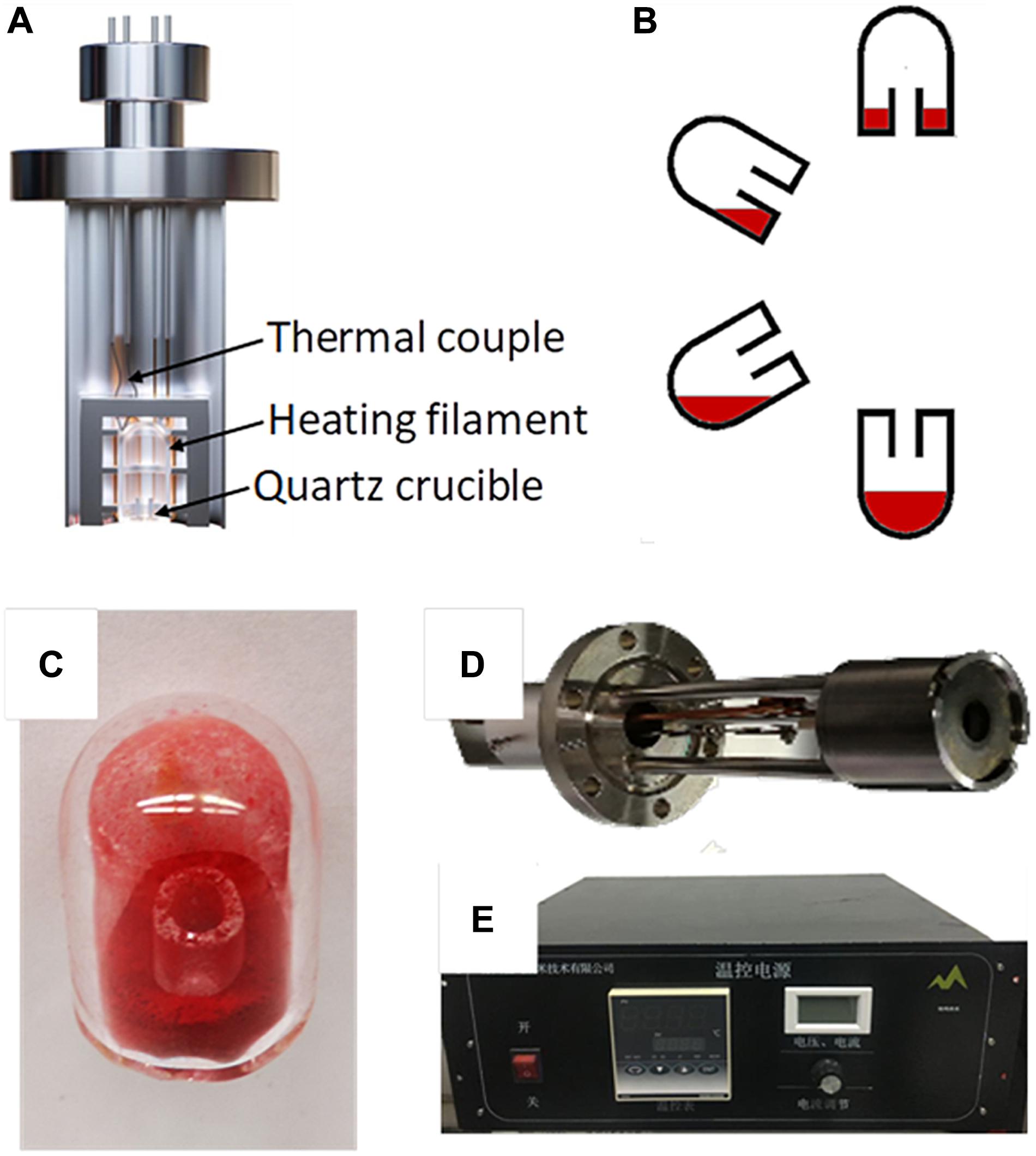
Figure 1. (A,B) Schematic of arbitrary mounting angle evaporator (AMAE) and loaded crucible at different angles and (C–E) photos of quartz crucible with loaded organic material, assembled AMAE, and supply unit, respectively.
Experimentally, we installed the AMAE in the top space of a home-made high vacuum deposition chamber, with the opening of the crucible facing down. The sample holder of the vacuum deposition system is attached to a manipulator which can rotate in 360°, enabling us to test and compare the results of AMAE with those of a commercial evaporator in the same chamber, as schematically shown in Figure 2A. Figure 2B shows the temperature curve measured by the thermal couple during the heating and cooling of the AMAE under a high vacuum of 10–5 Pa. For a setting from 100 to 400 °C that is the typical evaporation temperature for most functional organic molecules, the measured temperature was increased from room temperature to the target temperature in 3 min. Figure 2B further demonstrates excellent temperature control during the operation (variation less than ±0.2°C from 3 to 40 min) with target temperatures set at 100, 200, 300, and 400°C, respectively. The output, as described in the legend of the figure, is the setting limit of power during the operation for each setting temperature. After turning off the power supply, the temperature shows exponential decay with time and can reach below 75°C in 1 h without water cooling.
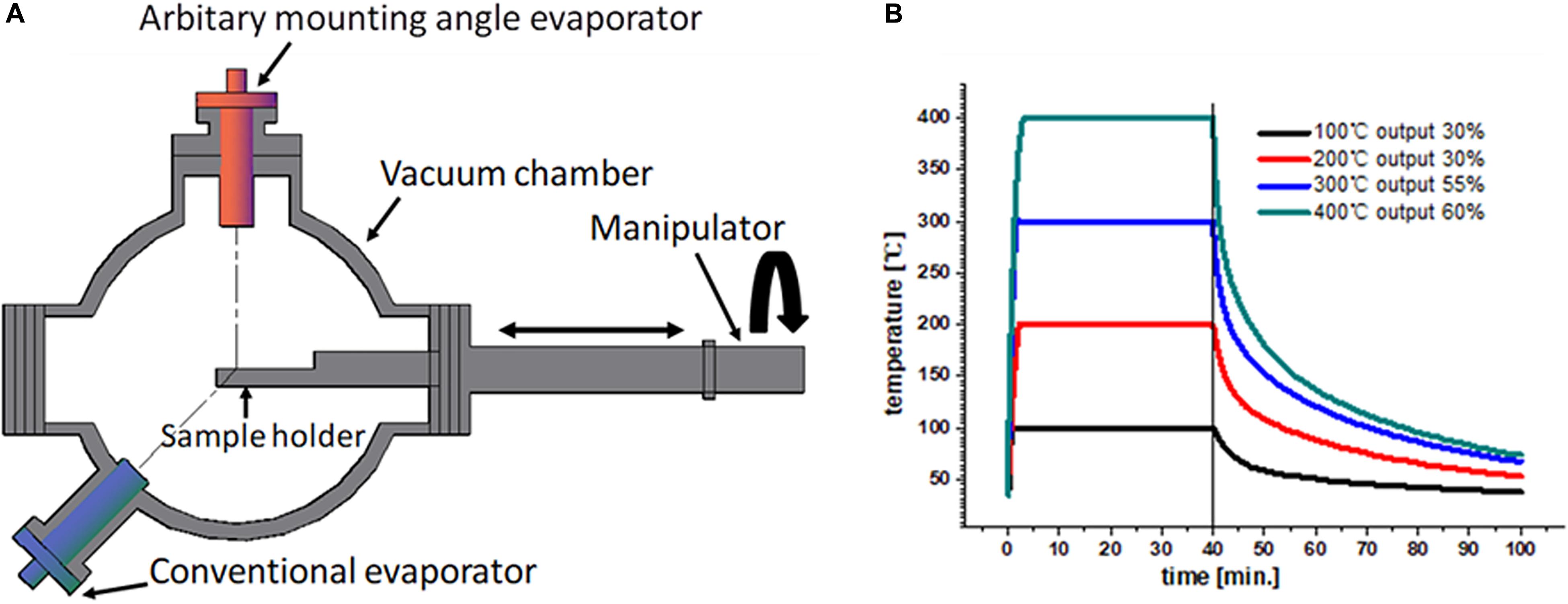
Figure 2. (A) Configuration of the testing vacuum chamber and (B) temperature curve of heating, operation, and cooling at different temperature settings.
Pentacene, a classic organic semiconductor extensively used for growth dynamics and OFET applications, was chosen for the demonstration of organic thin film deposition with AMAE (Heringdorf et al., 2001; Facchetti, 2007). The pentacene molecule was purchased from Aldrich and loaded to the crucibles of AMAE and conventional evaporator without further purification. The pentacene films were deposited onto 300 nm thermal oxidized SiO2 surfaces modified by trichloro(octadecyl)silane (OTS; Zhu et al., 2018). After deposition, the samples were taken out from the vacuum chamber for morphology characterization by AFM. Before field effect characterizations, the samples were transferred to another vacuum chamber to deposit Au source and drain electrodes through a shadow mask.
Results
Figures 3A,B show the typical AFM images of 30 nm Pentacene film deposited by the AMAE and conventional evaporator. The Pentacene films were deposited at a growth rate of 1 nm/min and substrate temperature of 60°C, which are optimized for OFET performances. Both films exhibit a typical dendrite structure that evolved from molecule absorption, diffusion, nucleation, and domain formation. The AFM images further show uniformly distributed and well connected molecule grains in the size of sub-micrometers to micrometers. The molecule grains, deposited either by AMAE or conventional evaporator, have a layered structure with a step height of 1.54 nm. Such a layered structure indicates that the Pentacene molecules are orientated with a standup configuration, which is consistent with those reported in the literature in studies that used similar deposition parameters (Du et al., 2012).
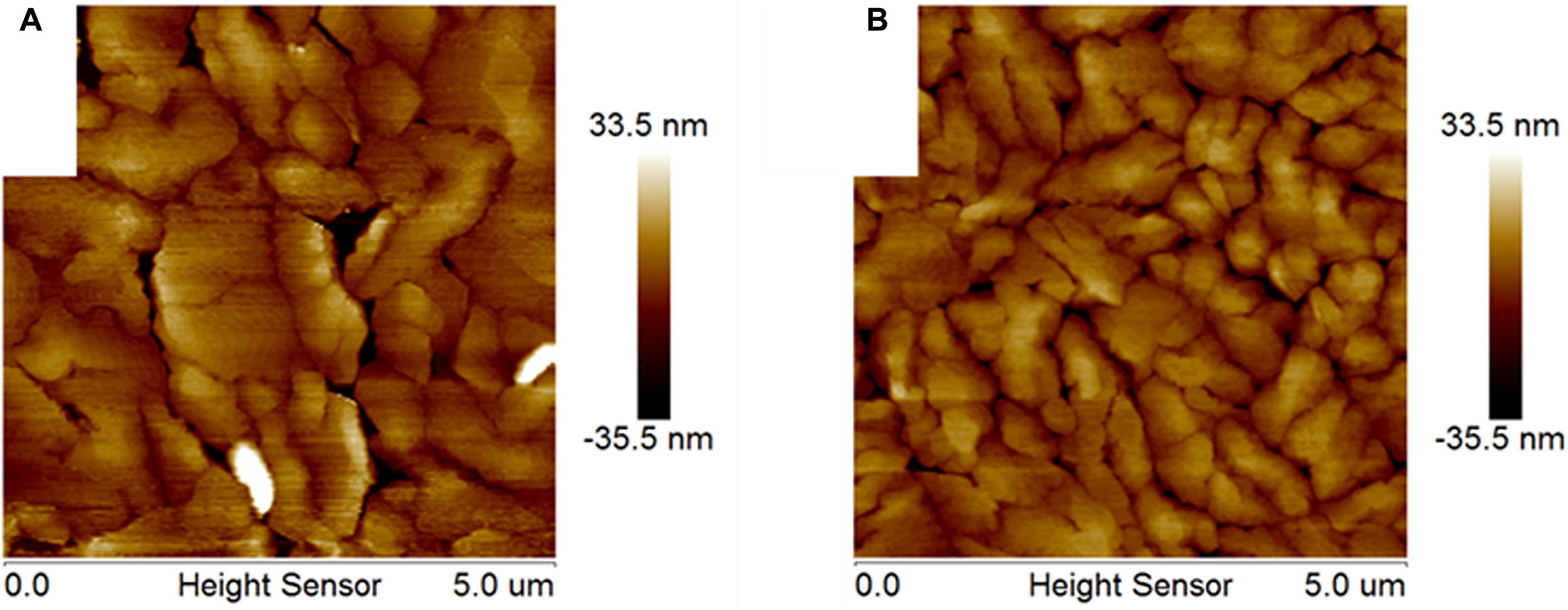
Figure 3. AFM images of 30 nm pentacene films on OTS modified SiO2 grown by; (A) AMAE and (B) conventional evaporator.
The electrical characteristics of the pentacene OFETs grown by AMAE and conventional evaporator were further characterized. After deposition of 30 nm pentacene films on OTS modified SiO2, Au source and drain electrodes were evaporated through a shadow mask, forming a bottom gate and top electrode OFET configuration. Figure 4 demonstrates the typical transfer and output curves of the OFETs with a channel length of 100 μm and channel width of 2000 μm. Figures 4A,B correspond to the performances of OFET deposited by AMAE, and Figures 4C,D show the device performance results by the conventional evaporator. As displayed from Figure 4, under the gate voltage of −50 V, AMAE transistor demonstrates an ON-state current of 63 μA, which is a little higher than that of a conventional device. The transistor parameters were further extracted using the following equation in the saturation region (Sharifi and Bazyar, 2011):
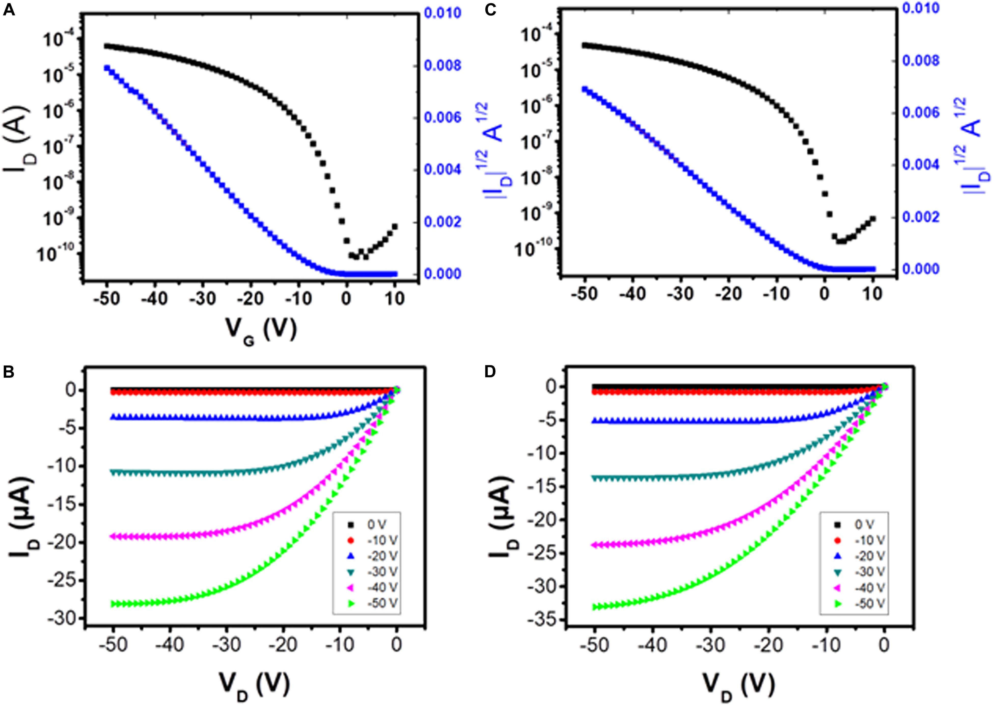
Figure 4. Transfer and output curves of the OFETs grown by (A,B) AMAE and (C,D) conventional evaporator.
Of which, Ci is the capacitance of 10 nf/cm2 for 300 nm SiO2, W is channel width, and L is channel length. The extracted charge mobility μ is about 0.38 cm2/Vs for the device grown by AMAE. In comparison, the device deposited by a conventional evaporator generates a charge mobility of 0.36 cm2/Vs. Both transistors present a similar threshold voltage around −10 V and Ion/off around 105–6.
For an organic vacuum evaporator, reproducibility is also a key aspect of its performace in thin film fabrication. We also performed 10 repeated experiments at the same deposition rate and substrate temperature on OTS modified 300 nm SiO2/Si for AMAE and conventional evaporator. The parameters of OFET deposited by AMAE show a narrower distribution range of mobility and threshold voltage than those by the conventional evaporator, as summarized in Table 1. Due to the crucible design of AMAE, molecules are firstly sublimated to the closed end of the crucible, which would rebound by the inner quartz wall back to the crucible or the outlet for film deposition. In this case, the molecules go through one or more reflections before depositing onto the substrate surface, which could lead to a more uniform distribution of a molecule beam and result in the narrow distribution range of transistor parameters. Owing to the high temperature of the closed end of the crucible, the rebounded molecule beam also bears high sublimation temperature and results in the relatively high mobility of OFETs fabricated by AMAE, as shown in Table 1.

Table 1. The transistor parameters of the films grown from AMAE and conventional evaporator.
Conclusion
In summary, we report an AMAE for organic semiconductor deposition, where the crucible is designed to prevent the loaded materials from falling. Thin film pentacene OFETs were deposited, fabricated, and characterized with AMAE and conventional evaporators, and exhibited comparable transistor performances, which demonstrates the feasibility of organic thin film growth from our AMAE technique. We present a new configuration and design, which allows the substrate to be put under the evaporator and to support shadow masking to avoid deformation. In addition, this technique will also enable the evaporator to be mounted at any specific angle for limited space.
Data Availability Statement
The raw data supporting the conclusions of this article will be made available by the authors, without undue reservation.
Author Contributions
WW and LC initiated the project. WW, LC, and LH designed and assembled the evporators. XS, YW, JL, and ZW performed the experiments. WW, LC, YW, and YC prepared the figures and manuscript. All authors contributed to the article and approved the submitted version.
Funding
This work was supported through the Transregional Collaborative Research Centre TRR 61/PAK943 by the DFG and by NSFC (21661132006 and 51821002), National Natural Science Foundation of China (21527805), as well as by the National Key R&D Program from MOST (2018YFE0200700).
Conflict of Interest
The authors declare that the research was conducted in the absence of any commercial or financial relationships that could be construed as a potential conflict of interest.
References
Annese, E., Santos, J. E. D., Rodrigues, G. L. M. P., Rocha, A. S., Moraesa, H. R. D., and Cezara, J. C. (2018). Ultrahigh-vacuum organic molecular-beam deposition system for in situ growth and characterization. J. Synchrotron Rad. 25, 1658–1663. doi: 10.1107/S1600577518011955
Dong, H., Fu, X., Liu, J., Wang, Z., and Hu, W. (2013). 25th Anniversary Article: Key points for high-mobility organic field-Effect transistors. Adv. Mater. 25, 6158–6183. doi: 10.1002/adma.201302514
Du, C., Li, L., Wang, W., Zhang, J., Yan, D., Hu, W., et al. (2012). Growth of large-size-two-dimensional crystalline pentacene grains for high performance organic thin film transistors. AIP Advances 2:022138. doi: 10.1063/1.4723851
Facchetti, A. (2007). Semiconductors for organic transistors. Mater. Today. 10, 28–37. doi: 10.1016/S1369-7021(07)70017-2
Forrest, S. R. (2004). The path to ubiquitous and low-cost organic electronic appliances on plastic. Nature 428, 911–918. doi: 10.1038/nature02498
Heringdorf, F.-J. M. Z., Reuter, M. C., and Tromp, R. M. (2001). Growth dynamics of pentacene thin films. Nature 412, 517–520. doi: 10.1038/35087532
Kan, J., Wang, S., Wang, Z., Guo, S., Wang, W., and Li, L. (2018). Fabrication of flexible thin organic transistors by trace water assisted transfer method. Chin. Chem. Lett. 29, 1681–1684. doi: 10.1016/j.cclet.2018.07.015
Kelley, T. W., Baude, P. F., Gerlach, C., Ender, D. E., Muyres, D., Haase, M. A., et al. (2004). Recent progress in organic electronics: materials, devices, and processes. Chem. Mater. 16, 4413–4422. doi: 10.1021/cm049614j
Kim, C., Kim, K., Kwon, O., Jung, J., Park, J. K., Kim, D. H., et al. (2020). Fine metal mask material and manufacturing process for high-resolution active-matrix organic light-emitting diode displays. J. Soc. Inf. Display. 28, 668–679. doi: 10.1002/jsid.901
Li, J., Hu, Y., Liang, X., Chen, J., Zhong, L., Liao, L., et al. (2020). Micro organic light emitting diode arrays by patterned growth on structured polypyrrole. Adv. Optical Mater 8:1902105. doi: 10.1002/adom.201902105
Ling, M. M., and Bao, Z. (2004). Thin Film Deposition, Patterning, and Printing in Organic Thin Film Transistors. Chem. Mater. 16, 4824–4840. doi: 10.1021/cm0496117
Matsui, H., Takeda, Y., and Tokito, S. (2019). Flexible and printed organic transistors: From materials to integrated circuits. Org. Electron. 75:105432. doi: 10.1016/j.orgel.2019.105432
Quiroga, S. D., Shehu, A., Albonetti, C., Murgia, M., Stoliar, P., Borgatti, F., et al. (2011). A high-vacuum deposition system for in situ and real-time electrical characterization of organic thin-film transistors. Rev. Sci. Instrum. 82:025110. doi: 10.1063/1.3534007
Sharifi, M. J., and Bazyar, A. (2011). Pentacene-based organic field-effect transistors: analytical model and simulation methods versus experiment data. ACEEE Int. J. Control Syst. Instrum. 02, 18–22.
Tang, C. W., and VanSlyke, S. A. (1987). Organic electroluminescent diodes. Appl. Phys. Lett. 51, 913–915. doi: 10.1063/1.98799
Tsumura, A., Koezuka, H., and Ando, T. (1986). Macromolecular electronic device: Field-effect transistor with a polythiophene thin film. Appl. Phys. Lett. 49, 1210–1212. doi: 10.1063/1.97417
Yuan, Y. B., Giri, G., Ayzner, A. L., Zoombelt, A. P., Mannsfeld, S. C. B., Chen, J. H., et al. (2014). Ultra-high mobility transparent organic thin film transistors grown by an off-centre spin-coating method. Nat. Commun. 5:3005. doi: 10.1038/ncomms4005
Zhu, J., Li, J., Zhong, Q., Wang, H., Huang, L., Fontein, F., et al. (2019). Lithography compatible, flexible micro-organic light-emitting diodes by template-directed growth. Small Method. 3:1800508. doi: 10.1002/smtd.201800508
Keywords: organic field effect transistors, vacuum deposition, evaporator, organic semiconductors, carrier mobility
Citation: Shen X, Wang Y, Li J, Chen Y, Wang Z, Wang W, Huang L and Chi L (2020) Performances of Pentacene OFETs Deposited by Arbitrary Mounting Angle Vacuum Evaporator. Front. Mater. 7:245. doi: 10.3389/fmats.2020.00245
Received: 03 June 2020; Accepted: 03 July 2020;
Published: 16 September 2020.
Edited by:
Deyang Ji, Tianjin University, ChinaCopyright © 2020 Shen, Wang, Li, Chen, Wang, Wang, Huang and Chi. This is an open-access article distributed under the terms of the Creative Commons Attribution License (CC BY). The use, distribution or reproduction in other forums is permitted, provided the original author(s) and the copyright owner(s) are credited and that the original publication in this journal is cited, in accordance with accepted academic practice. No use, distribution or reproduction is permitted which does not comply with these terms.
*Correspondence: Wenchong Wang, d2FuZ3dAdW5pLW11ZW5zdGVyLmRl; Lizhen Huang, bHpodWFuZ0BzdWRhLmVkdS5jbg==; Lifeng Chi, Y2hpbGZAc3VkYS5lZHUuY24=