 Partha Kumbhakar1
 Chinmayee Chowde Gowda
 Chandra Sekhar Tiwary
- 1Department of Metallurgical and Materials Engineering, Indian Institute of Technology Kharagpur, Kharagpur, India
- 2School of Nano Science and Technology, Indian Institute of Technology Kharagpur, Kharagpur, India
In the last several decades, significant efforts have been devoted to two-dimensional (2D) materials on account of their optical properties that have numerous applications in the optoelectronic world in the range of light-emitting diodes, optical sensors, solar energy conversion, photo-electrochemical cells, photovoltaic solar cells, and even the biomedical sector. First, we provide an outline of linear optical properties of 2D materials such as graphene, TMDs, h-BN, MXenes, perovskite oxide, and metal-organic framework. Then, we discuss the optoelectronic properties of the 2D materials. Along with these, we also highlight the important efforts in developing 2D optical materials with intensive emission properties at a broad wavelength from ultraviolet to near-infrared. The origin of this tunable emission has been discussed decoratively. Thickness and layer-dependent optical properties have been highlighted and are explained through surface defects, strain, vacancy, doping, and dangling bonds emerging due to structural change in the material. The linear and nonlinear optical properties in 2D MXene and perovskite oxides are also impressive due to their potential applications in next-generation devices with excellent optical sensitivity. Finally, technological innovations, challenges, and possible tuning of defects and imperfections in the 2D lattice are discussed.
Introduction
Optical properties have been one of the most fascinating and functional aspects of any nanomaterial. They are generally customized by altering parameters such as particle size, shape, surface characteristics, and various other variables (Xia et al., 2014; Sun et al., 2016). Major application fields based on optical properties include light emission and detection, solar cells, photocatalysis, photoelectronic and imaging, and biosensing. The basic understanding of the fundamental optical properties and related spectroscopic techniques can help distinguish the nanomaterial. For example, when the particle size reduces, shifting of absorption and photoluminescence (PL) emission spectra of semiconductor nanoparticles is observed, which is also conferred in other semiconductor and metal nanomaterials (Kelly et al., 2003; Zhang and Wang, 2017). The electronic transition between the conduction band (CB) and valence band (VB) results in optical properties such as PL emission and absorption. The reduced dimensionality of the material has a significant impact on the electronic structure of these bands. During PL emission, the incident light leads to absorption of electrons and then these excited electrons drop to a lower energy level from the excited energy states. Additionally, in a semiconductor nanomaterial, PL emission studies help determine the concentration of impurities, defects, energy levels, and fundamental emission processes. Impurities introduced in the semiconductors lead to several energy level formations within the bandgap of these materials. Unlike conventional semiconductor materials, the 2D semiconductor materials act as a good charge acceptor or donor, resulting in the attractive optical property of these materials. Similarly, change in dimensionality in 2D materials show enhanced electronic and optoelectronic properties and find applications in ultrafast carrier dynamics, varied bandgap energies, tunable emission properties, high carrier mobility, and confined electronic and magnetic effects (Wang et al., 2017; Tan et al., 2020). Unique properties such as ultrafast photonics, which are due to physical singularities occurring from heat transfer and charge, have also gained broad scope amongst 2D materials. Along with linear optical properties, nonlinear optical properties are also interesting in 2D materials. Due to the optical nonlinearity of these materials, the saturable absorbers can periodically modulate the circulating light field in the laser cavity (Liu et al., 2020).
Reviews exist on the discussion of linear optics, nonlinear optics, light-emitting, photodetection, and anisotropy in 2D materials, as shown in Figure 1 (Xia et al., 2014; Mak and Shan, 2016; Guo et al., 2019; Wang C. et al., 2020). A recent review was published discussing the tunable properties of 2D materials (Ma et al., 2021). We have focused our discussion on graphene-based optical device applications. Graphene’s optical properties are quite unique, with band structure having van Hove-like singularities. Chiral symmetry also exists for the quasiparticles, which helps fix the direction of pseudospin to be parallel for electrons or antiparallel for holes (Grigorenko et al., 2012), whereas in monolayer TMDCs, optical absorption is dominated by direct transitions between VB and CB states around the K and K′ points. Direct band-to-band transitions in 2D are characterized by a step function-like spectrum originated from the energy-independent joint-density-of-states and transition matrix elements near parabolic band edges (Mak and Shan, 2016). Later, hexagonal boron nitride (h-BN) was studied for light-matter interactions at the atomic scale (Latini et al., 2017). Device applications of black phosphorus (BP) were discussed in the later section. BP’s atomic structure is folded, resulting in high anisotropy of phonons, photons, and electrons (Qiao et al., 2014). Here, in this review, we have focused on the recent technological innovations in 2D materials such as h-BN, BP, MXenes, perovskite oxides, and metal-organic framework nanosheets (MONs). A wide variety of optical device applications, recent theoretical first-principle calculations, and future advancements in device applications have been discussed.
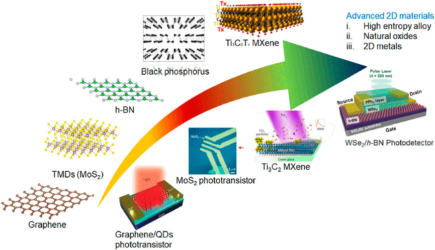
FIGURE 1. Overview of different types of 2D materials and their optoelectronic applications. [adapted and modified from (Konstantatos et al., 2012; Yin et al., 2012; Jo et al., 2016; Chertopalov and Mochalin, 2018)]
Results and Discussions
Advanced Optical Property and Photonic Applications of Graphene
Graphene is one of the pioneers in the field of 2D materials. Light-matter interaction in graphene gives rise to exciting optical properties and has impacted optoelectronics, nanoelectronics, and the nonlinear optics world, as depicted in Figure 2. The linear absorption of graphene shows an absorption band centered at ∼260 nm due to π-π* transition of electrons in π-conjugated sp2 carbon core (Pramanik et al., 2018; Zhu B. et al., 2018). Graphene does not show any visible luminescence. Previously, several researchers have studied the use of graphene in ultrafast and efficient optical switching, solar cell, optical modulators, plasmonic devices, transparent light emitters, displays with low operation voltage, ultrafast optical communications, and state-of-the-art photodetectors (Liu et al., 2011; Grigorenko et al., 2012; Gan et al., 2013; Kim et al., 2015), as shown in Figure 2. It is believed that absorption property in the UV region may have huge applications in solid-state lighting (Chen et al., 2018). Recently, optical switching gained massive attention as it overcame the limitations of electrical switching (Ono et al., 2020). Notami et al. greatly enhanced the nonlinear absorption of graphene loaded with plasmonic waveguides and achieved ultrafast optical switching with switching energy and time of 35 fJ and 260 fs, respectively, connected to conventional waveguides for use in integrated circuits (Ono et al., 2020). Studies exist in the field of biological molecule sensing of nucleic acids using deformed graphene by FET-based biosensors (Hwang et al., 2020). In another study, computational simulations revealed “electrical hot spots” in the sensing channel, which reduces the charge screening. Recently, meter-scale level optical fiber was demonstrated by a combination of graphene and photonic crystal fiber, and it shows broadband response and significant modulation depth under a low gate voltage (Chen et al., 2019). Recent studies of composite graphene and W- and Mo-based TMD heterostructures are reported to form electroluminescent systems with linewidths approaching homogeneous limits near the THz rate. The spatially localized hot electrons (∼2,800 K) resulted in a 1000-fold enhancement in thermal radiation efficiency (Kim et al., 2015; Lorchat et al., 2020). Distinct nonlinear nano-optical properties of graphene are also well-reported, with enhanced broadband four-wave mixing response in fs nano-imaging being revealed. The strong electron-electron interaction was also recently studied (Jiang et al., 2019). Other graphitic structures like reduced graphene oxide (rGO) infused nanofluid were also explored for their optical filtration of solar energy and thermal efficiencies reaching up to 30%. They influence the functionality of hybrid solar cells (Abdelrazik et al., 2020b). In UV-Vis absorption spectra measurements, the hydrophobic nature of rGO improved the dispersion stability. The nanoparticle concentration on the spectral transmittance effects decreased with the increase in the concentration. UV-Vis absorption also revealed that the water/rGO-Ag samples display consistency in α in the relatively higher value range of 1.5–4 eV and then gradually increase further as bandgap increases.
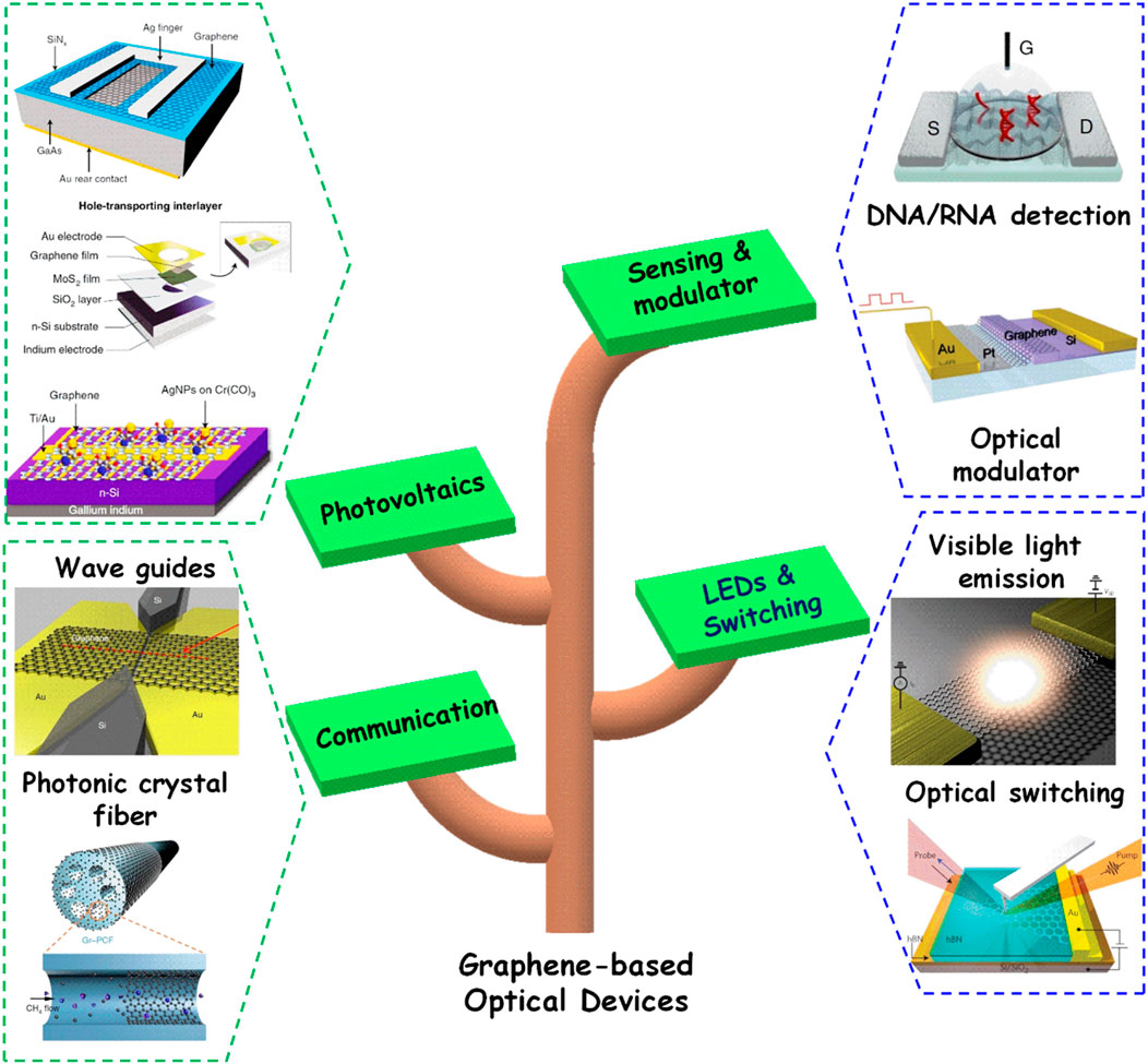
FIGURE 2. Schematic representation of graphene-based optical device applications [adapted and modified from (Kim et al., 2015; Ni et al., 2016; Chen et al., 2019; Behura et al., 2019; Ono et al., 2020; Hwang et al., 2020)].
Device Applications of Transition Metal Di-Chalcogenides
2D transition metal di-chalcogenides (TMDs) consist of over 40 compounds with the general formula of MX2 (X = S, Se, and Te). Primarily group VI TMDs are extensively studied, and their several optical applications have been obtained. Manipulation at the atomic scale, ultrathin thickness, and their band gaps enable TMD’s light-matter interaction study. Some of them include MoS2, WS2, MoSe2, ReS2, MoTe2, and WTe2, synthesized by various approaches (Chen et al., 2018). Their reduced dimensionality makes 2D TMDs fascinating with strong light-matter interaction and enhanced optical properties. Varied lateral sizes and the number of layers are observed in 2D TMDs. From the literature, the bandgap decreased by ∼0.3–0.35 eV as the layer number increased from monolayer to bulk in Mo- and W-based TMDs, showing weak dependence of optical band gap on layer number (Synnatschke et al., 2019).
Sulfides
The optical absorption of exfoliated molybdenum sulfide (MoS2) layer has been investigated by several researchers, and the major excitonic absorption peaks are observed at higher wavelength regions (Figure 3A) (Vikraman et al., 2017). MoS2 monolayer has a stable, gate tunable optical response at RT near excitonic transition (Kravets et al., 2019). It also shows strong excitonic PL emission in the higher wavelength region (Figure 3E). Hybrid nanostructures of MoS2 show enhancement in polarisation near exciton binding energies (Eda et al., 2011). Other TMD alloys of Mo-, like MoxW1−xSe2 and WS2ySe2(1−y), exhibit enhanced PL emission in the monolayers which is due to deep trap states produced by vacancies that promote the emission of excitons and trions (Sun et al., 2017). Theoretical calculations also confirmed the experimental results. MoS2 with four different morphology-controlled plasmonic nanoparticles was studied. Furthermore, the plasmonic strain blueshifts the bandgap by 32 times and enhanced photoresponse due to massive hot electron injection (Sriram et al., 2020). An asymmetric Fabry−Perot cavity was formed based on a hybrid structure of MoS2/hBN/Au/SiO2 by vertical stacking. PL intensity of monolayer MoS2 is enhanced over two orders. The strong absorption was justified from photonic localization on the top of the microcavity (Wang et al., 2017).
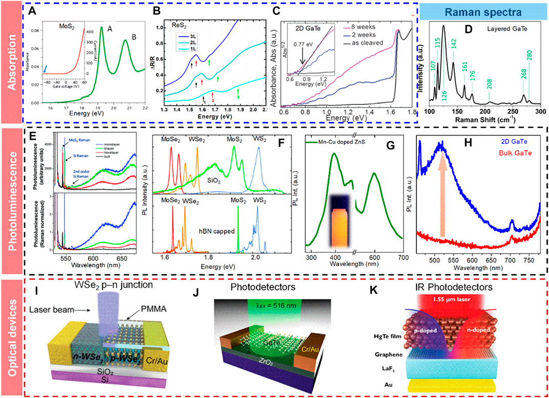
FIGURE 3. (A) Absorption spectra of monolayer MoS2 [adapted and modified from (Vikraman et al., 2017)]. (B) Layer-dependent reflectance spectra of ReS2 [adapted and modified from (Zhao K. et al., 2018)]. (C) Absorption spectra of layered GaTe with and without oxidation. Inset shows the change in bandgap due to oxidation [adapted and modified from Fonseca et al.,2016]. (D) Raman spectra of GaTe [adapted and modified from (Huang et al., 2016)]. (E) PL emission spectra of monolayer MoS2 with Raman signal [adapted and modified from (Eda et al., 2011)]. (F) PL emission spectra of MoS2, WS2, MoSe2, and WSe2 in the different substrates [adapted and modified from (Cadiz F. et al., 2017)]. (G) Yellow-orange emission of layered ZnS. Inset shows the digital photograph of the sample signal [adapted and modified from (Kumbhakar et al., 2019)]. (H) Comparison PL emission spectrum of bulk and 2D GaTe [adapted and modified from (Siddique et al., 2021)]. Schematic diagram of (I) WSe2 based p-n junction [adapted and modified from Sun et al., 2020], (J) GaTe photodetector [adapted and modified from (Kang J. et al., 2018)] , and (K) IR photodetector using HgTe [adapted and modified from (Noumbé U. N. et al., 2020)].
The layered dependent optical reflectance spectra ReS2 are presented in Figure 3B. It shows that the peak positions change with layer number. Temperature effects varied the optical bandgap of the ReS2 films (10 layers); the bandgap varied from 1.36 eV (303 K) to 1.38 eV (383 K). Theoretical predictions showed similar results where the bandgap increased from 1.32 to 1.40 eV. Energy level degeneracy was explained by coupling between the Re 5d orbital and S 3p orbital being weaker because of which the energy level splitting is smaller with increased temperature (Zhao K. et al., 2018).
Monolayer WS2 onto exfoliated graphite by high-temperature CVD showed a single excitonic PL peak with a Lorentzian profile at RT and 8 meV bandgap at 79 K. In a similar study, temperature-dependent PL spectra of WS2 on different substrates was analyzed (Kobayashi et al., 2015). Similarly, PL emission spectra of MoS2 and WS2 were also studied on two different substrates, and it is observed that with hBN, PL emission shows more narrowing behavior (Figure 3F Noumbé U. N. et al., 2020). Studies with multi-atom doped ZnS high fluorescence efficiency of ∼62% in the visible region. An intense stable yellow-orange emission was observed at RT for Mn Cu co-doped sample under UV-light as shown in Figure 3G (Kumbhakar et al., 2019).
Selenides
Some of the 2D selenides have applications in a wide range of optical devices. The bandgap transition from direct to indirect was noted when the thickness of the layers (L) is reduced to <6 nm. When L decreases below ∼10 nm, the PL intensity decreases by a factor >10. This value is significantly larger than that for any other luminescent material. At this thickness, the optical bandgap was found to be 1.44–1.47 eV (Mudd et al., 2013). An encapsulated InSe device offers high quality and ambient-stable mobility of 30–120 cm2 V−1 s−1 compared to ∼1 cm2 V−1 s−1 (un-encapsulated devices). For complete h-BN encapsulation to GaSe, PL with a photoresponsivity of 84.2 A W−1 (at 405 nm) was observed (Zhang et al., 2019). Based on the anisotropic nonlinear behavior of the material, a SnSe-based all-optical switch was proposed. The nonlinear optical response was polarization-dependent, and an unexpectedly high on/off ratio was achieved (Zhang et al., 2019). In another study, the SnSe-decorated nonlinear device in fiber lasers with ultrashort mode-locked pulses at 1.5 and 2.0 μm was fabricated. Additionally, studies indicated that the material could serve as a good saturable absorber for lasers in the broadband area (Wang Z. et al., 2020).
Tellurides
2D tellurides are seldom explored for their optical properties compared to other chalcogenides. Layered Si2Te3 and Mn-Si2Te3 have been studied for their high-pressure optical phonon behavior. Raman modes in Mn-Si2Te3 show phonon stiffening and softening, suggesting negative linear compressibility (Johnson et al., 2019). In-plane optical anisotropy and RT PL spectrum in the visible spectrum range were observed in the 2D GaTe sample (Figure 3H). A GaTe multilayer study showed weak anisotropy in the visible spectrum range, and the Raman intensity depended on crystalline orientation (Figure 3D). These results suggest high photoresponsivity and the possibility of the generation of a large number of dangling bonds providing recombination sites for carriers in low dimensional structures (Huang et al., 2016; Siddique et al., 2021). Monolayer GaTe based on DFT calculations gave unique optical properties because of the anisotropy layer affecting bandgap and absorption coefficient (Abed Al-Abbas et al., 2018). The optical absorption in the visible region with high electron and hole mobilities was observed for the monolayer of GeTe. It also shows a large bandgap which is strain-tunable compared to its bulk form (Qiao et al., 2018). GaTe nanoflakes also showed enhanced performance as photodetectors exhibiting better responsivity and illuminating properties, the device is as depicted in Figure 3J (Kang J. et al., 2018). An enhanced photo detection range and faster response time was noted with a combination of HgTe and graphene structure. The device structure is as shown in the Figure 3K. The structure constructed on LaF3 substrate offers high gate tunablity and possible charge carrier polarities in graphene and HgTe. (Noumbé U. N. et al., 2020)
Optical Properties and Emerging Applications of Hexagonal Boron Nitride
With highly dispersive surface phonon-polariton modes, hexagonal boron nitride (hBN) is a natural hyperbolic material. Raman spectra of mono-, bi-, and trilayer BN show a characteristic peak of E2g phonon mode, analogous to the G peak of graphene (Taylor, 1988). A progressive weaker peak is observed as layer number decreases which are ∼50 times smaller than for graphene’s G peak in monolayer BN, under the same measurement conditions as seen in Figure 4A. Strain effects on hBN are pretty interesting. The phonon frequency shifts are due to compressive strain in hBN contrast with near-field IR (Figure 4B). Figure 4E illustrates local strain measurement in annealed hBN flakes of ∼6 nm thickness on a SiO2/Si substrate. The first-principles calculation results under isotropic biaxial strain, hBN TO phonon frequency shift was also studied for the same material (Figure 4F) (Lyu et al., 2019). Theoretical and experimental optical properties of heterostructures of hBN with other 2D materials are also studied. Theoretically, studies of graphene-hBN heterostructure were studied by Kumar et al. Regarding the interaction of graphene plasmon and hBN phonon, its emission properties are studied in detail. Figure 4C depicts monolayer graphene on hBN film with the details mentioned in the figure. Also, Figure 4D shows the permittivity of hBN, and the result shows a possibility of hyperbolicity (Kumar et al., 2015). A Van der Waals (vdW) WS2/MoS2 heterostructure on hBN flake showed excitonic optical responses. This was mapped to the presence of several valleys in the electronic structure. At 1.3–1.7 eV (at RT), PL emission was observed, generally absent in WS2 or MoS2 monolayers alone. The theoretical analysis concluded that the PL peaks originated in monolayer hBN and were due to the following: (I) direct K−K interlayer excitons, (II) indirect Q−Γ interlayer excitons, and (III) indirect K−Γ interlayer excitons. The level alignment was also calculated and had good agreement with experimental PL spectra (Latini et al., 2017).
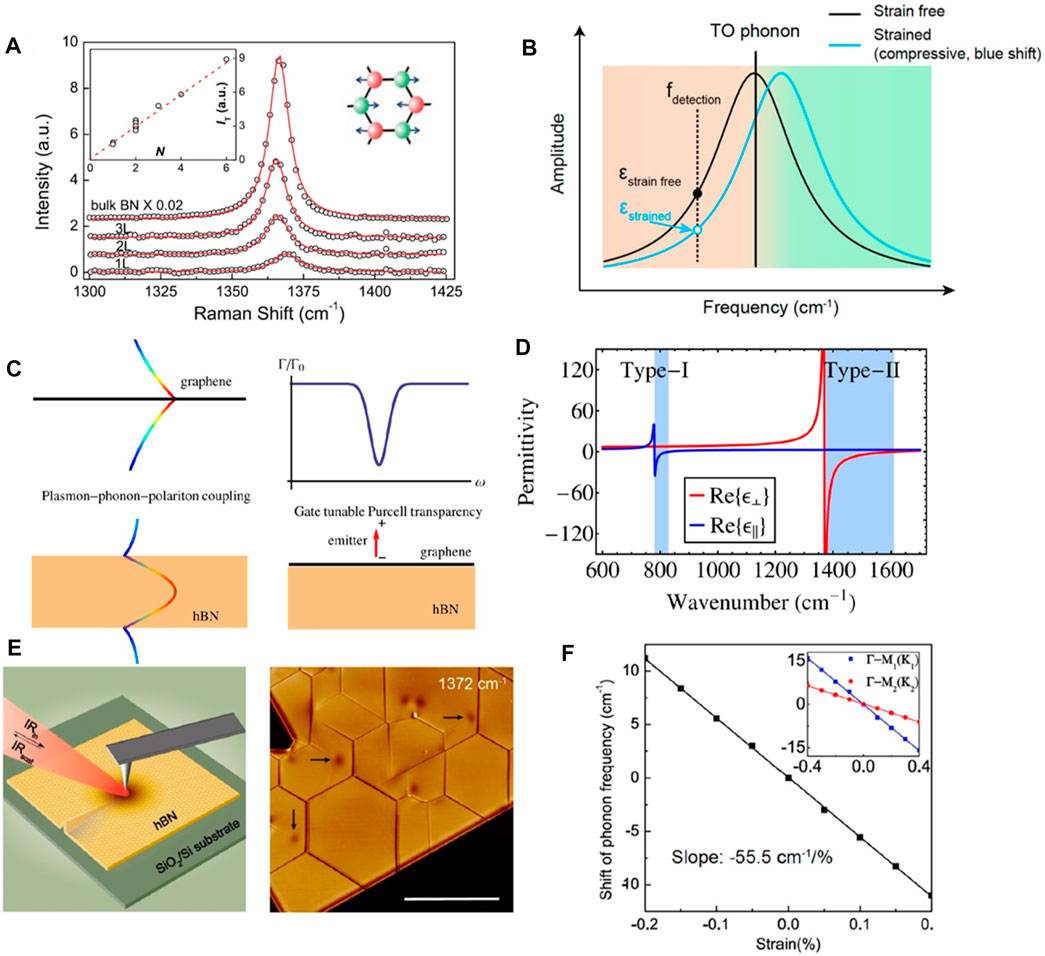
FIGURE 4. (A) Raman spectra of hBN. Inset shows the changes in integrated intensity with the layer number. The picture in the top right side shows phonon mode for Raman peak [adapted and modified from (Lyu et al., 2019)]. (B) Illustration of compressive strain induced phonon frequency shift and near-field IR contrast [adapted and modified from (Lyu et al., 2019)]. (C) The interaction of graphene plasmon with hBN phonon (left) and emission of a nearby dipole into hybrid modes (right) [adapted and modified from [(Kumar et al., 2015)]. (D) Permittivity of hBN [adapted and modified from (Kumar et al., 2015)]. (E) The near-field IR measurement technique using hBN [adapted and modified from (Lyu et al., 2019)]. (F) Theoretical results of phonon frequency as a function of isotropic strain [adapted and modified from (Lyu et al., 2019)].
In graphene-hBN heterostructures, we observed hybridization of plasmon and phonon, as well as the reduction of the group velocity of light in the IR region, and this was because of strong plasmon dipole−dipole coupling. Tuning the coupling strength can open a new area to control light and detection in the mid-IR window. Plasmon−phonon polaritons in these heterostructures were also studied (Jia et al., 2015).
Exciting Nonlinear Optical and Luminescence Properties of Layered Black Phosphorus
Black phosphorus (BP) was investigated as 2D material recently offering high mobility and thickness-dependent direct bandgap. Multilayer BP sheets on periodic stress modulate their optoelectronic properties. The material also offers a better strain tunability than TMDs offering low-temperature periodic stress modulation yielding quantum confinement. BP finds a wide range of application areas, including photovoltaics and optoelectronics (Quereda et al., 2016).
Optical conductivity was studied for a single layer and bulk BP at varied applied strain along zigzag (σZZ) and armchair (σAC) directions. Similarly, wavelength and pulse-dependent nonlinear optical properties of BP nanosheets have been studied by several researchers. The SA response in the visible range was better than the near-IR range. Figure 5A shows absorption spectra of the BP dispersed in ethanol (Huang et al., 2017). Reports of encapsulation technique usage showed reduced exciton binding energy by 70% in monolayer and elimination of the bound exciton in the four-layer BP structure. This changes the nature of the excited states and absorption spectrum (Qiu et al., 2017).
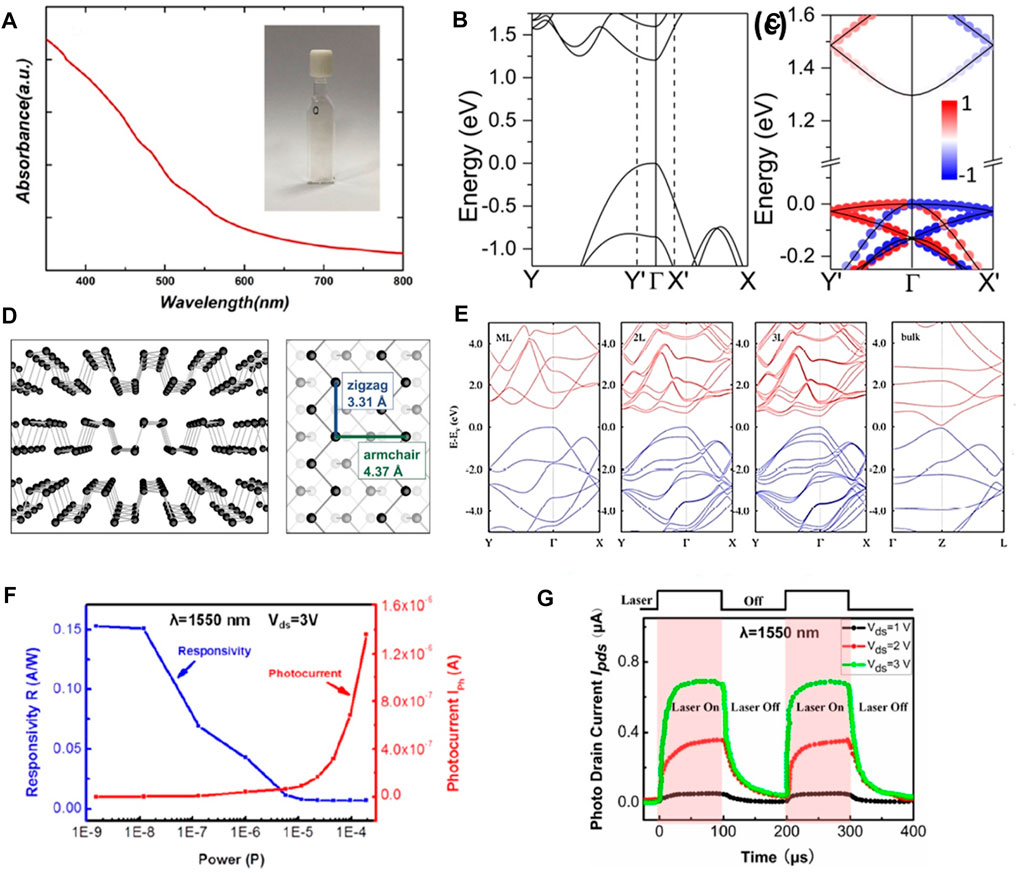
FIGURE 5. (A) UV-Vis absorption spectrum of the BP. Inset shows the digital photograph of the BP dispersion [adapted and modified from (Huang et al., 2017)]. (B) GW quasiparticle band structure of naturally stacked bilayer BP and (C) 90° twisted bilayer BP [adapted and modified from (Cao et al., 2016)]. (D) Crystal structure of BP [adapted and modified from Zahn et al., 2020)]. (E) Calculated electronic band structures of BP with different thicknesses [adapted and modified from (Lu et al., 2016)]. (F) The photocurrent (IPh) and photoresponsivity (R) of BP and (G) Time-resolved photoresponse of the junction photodiode [adapted and modified from (Ye et al., 2016)].
Size-dependent nonlinear optical response of BP nanosheets synthesized by LPE for nanosecond laser pulses was reported recently. Results showed that the nonlinear absorption coefficient of BP depended on laser intensity and lateral flake dimension (Szydłowska et al., 2018). Other major application areas of BP include switchable electronic circuits. A switchable gate voltage led to switchable optical linear dichroism. Figure 5B shows GW quasiparticle of stacked BP, and Figure 5C shows 90° twisted BP with a 2-fold degeneracy (Cao et al., 2016). Enhanced photoresponsivity of a BP-based photodetector with a high photocurrent ratio (∼8.7) was obtained. Thus, BP has potential applications in telecommunication, sensing, and IR polarimetry imaging (Venuthurumilli et al., 2018). The current-rectifying behavior can be in the heterojunction of BP/MoS2 photodetector by tuning the gate voltage and forward-to-reverse bias current ratio exceeding 103. Figure 5F shows photocurrent (IPh) and photoresponsivity (R) of the junction under the wavelength of 1.55 μm, at Vds = 3 V. Figure 5G shows the photoresponse of the junction at a different voltage (Ye et al., 2016).
Theoretical and experimental anisotropic studies of the material also exist due to atomic vibrations at increased temperatures as well as in RT. Figure 5D illustrates the anisotropic crystal structure of BP (Villegas et al., 2016; Zahn et al., 2020). Strain-induced anisotropy resulted in electron−phonon interaction behavior in strained BP (Zhu W. et al., 2018), and a high PL lifetime of BP as suitable candidates for live-cell imaging has been studied (Meng et al., 2018). Figure 5E shows a representation of electronic band structures of BP with different thicknesses (Lu et al., 2016).
Optoelectronic Properties of Carbonitride MXene
2D transition metal carbides and nitrides (MXenes) have gained massive attention for optoelectronic applications. Higher conductivity, tunable electronic structure, optical nonlinearity, and ease of fabrication make MXenes interesting 2D material to work with. Application areas include optoelectronic devices as well as energy storage, electromagnetic shielding, etc. 2D titanium carbide is the most explored MXene, with the highest value of electronic conductivity (10,000 S cm−1). A study on partially oxidized MXene (titanium oxide) showed photoresponse in the UV spectrum region (Figure 6A) (Chertopalov and Mochalin, 2018).
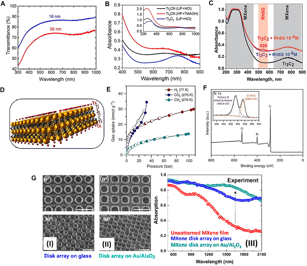
FIGURE 6. UV-Vis absorption spectra of (A) Ti3C2Tx films with a thickness of 16 and 38 nm [adapted and modified from (Chertopalov and Mochalin, 2018)], (B) d-Ti3CNTx [adapted and modified from (Hantanasirisakul et al., 2019)], and (C) pristine Ti3C2Tx in water and mixed with Rh6G dye [adapted and modified from (Sarycheva et al., 2017)]. (D) Structure of a single layer of Ti3C2Tx [adapted and modified from (Chaudhuri et al., 2018)]. (E) High-pressure gas (H2, CO2, and CH4) sorption isotherms of the V2D-BBL structure. (F) XPS survey of the V2D-BBL sample (inset: deconvoluted N1s spectrum) [adapted and modified from (Noh et al., 2020]. (G) SEM images collected from 0° (top) and 30° inclined angles (bottom) [adapted and modified from (Chaudhuri et al., 2018)].
Studies on 2D titanium carbonitride (Ti3CNTx) showed that the material possesses lower electronic conductivity and a blue shift is observed in the UV-Vis absorption spectra compared to Ti3C2Tx. Reports exist on intercalants (water and tetra-alkylammonium hydroxides) decreasing the electronic conductivity because of resistance between the flakes with varied temperatures giving rise to tunable electronic properties. The UV-Vis absorption spectra of Ti3CNTx solutions are shown in Figure 6B (Hantanasirisakul et al., 2019). The structures also showed enhanced dye degradation properties, as shown in Figure 6C (Sarycheva et al., 2017). A report on 2D Ti3C2Tx, enhancing Raman intensity from the dyes on a substrate and in solution was experimentally observed. The study suggested that MXene can increase the positively charged molecules and their potential biomedical/environmental applications. In another study, microcapsules for drug delivery assembled with a layer-by-layer strategy were explored (Stanciu et al., 2020). High-efficiency of optical absorption up to ∼90% for ∼1.55 μm wavelength window has been achieved in arrays of nanodisks made of Ti3C2Tx showing strongly localized SPR behavior at near-IR region. Figure 6D depicts the single-layer structure of Ti3C2Tx. Figure 6G shows SEM images of disk array (I) on glass and (II) on Au/alumina and (III) absorption spectra comparison for the two types of disk arrays and unpatterned MXene film (Chaudhuri et al., 2018). Figure 6E shows high-pressure gas (H2, CO2, and CH4) sorption isotherms of the vertical 2D layered benzimidazobenzophenanthroline structure at varying temperatures (Noh et al., 2020). Figure 6F depicts the XPS survey spectra of the unfolded peaks pertaining to the same structure. Ti3C2Tx combined with polyvinyl alcohol (PVA) nanocomposites were analyzed for their possible applications in the field of optoelectronics, conductive filler, and electromagnetic absorbers (Tan K. H. et al., 2021). PVA improved the electrical performance of the material up to ∼3,000 times as compared to pure PVA, with the highest σ value of 7.25 × 10⁻³ Sm−1. Furthermore, plasmon resonance in MXenes causes absorption in the visible light region. Ranging from the lowest Eg of 3.3 eV to the highest 4.2 eV was obtained in the PVA-MXene mixture due to modified energy states between the conduction and valence bands. In another interesting composite study, thermal and physical management were observed for MXene with palm oil nanofluid, and enhancement in these properties and the electrical efficiency increased to 13.8% and thermal efficiency by ∼11.2% of the solar PV/T system was studied (Samylingam et al., 2020). A similar study was also conducted with MXene based silicone oil nanofluids in increasing thermoelectric efficiency in solar cells (Aslfattahi et al., 2020b). Their optical properties and stability are also exciting to explore because of the wide range of optical absorption spectra offered by the material and the optical filtration of the composite materials (Abdelrazik et al., 2020a). Studies on organic phase change material and MXene structures are novel materials explored for their energy storage and conductivity enhancements (Aslfattahi et al., 2020a). The usage of MXene nanoparticles as additives showed variation in intermolecular dynamics of the paraffin wax in this particular study.
2D Perovskite Oxides and Organic-Inorganic Structures for Solar Cell Device Fabrication
Perovskites are high entropy oxides with multiple cation Wyckoff positions and find a wide range of applications in optical and electronic devices. The freestanding 2D monolayers of perovskites offer a tunable wide bandgap semiconducting material. Theoretical studies on some important perovskite oxides (ABO3), SrTiO3, LaAlO3, and KTaO3 were compared with graphene and MoS2 monolayer for their optical properties. Organic light-emitting diodes were also fabricated using calcium niobate (CaNbO3) nanosheets. With a wide bandgap of ∼3.5 eV, CaNbO3 has been used as electron transport layers (ETLs) and electron injection layers (EILs). The operational lifetime of the devices was exceptional, with high luminance. Figure 7D shows the tandem solar cell device structure (Li et al., 2010; Chang et al., 2012). The bandgap change was not observed for [TBAxH1−x] + [Ca2Nb3O10]− nanosheets obtained through intercalation−exfoliation of KCa2Nb3O10. The structure was preserved after delamination, and the bandgap values helped analyze the electronic structure. And the intensity of the plasmon excitation increased, for which the basis was increased thickness (Virdi et al., 2016). Many studies on perovskite structures aiding other applications such as photocatalysis and visible photoelectrochemical oxidation due to the varied optical bandgap and accelerating the interfacial charge transfer process have been explored in recent years. Figure 7C shows band structures of restacked KCa2Nb3O10, KCaSrNb3O10, and KSr2Nb3O10 with conduction band energies of −0.5, −0.4, and −0.3 eV, respectively (Oshima et al., 2016; Opoku et al., 2017). 2D perovskite solar cell estimates that the charge recombination rate constants are larger than the 3D compound. The charge-carrier recombination in the planar device architecture was particularly noted for (BA)2 (MA)4Pb5I16. Figure 7A shows the UV-Vis absorption spectra of the films on the glass substrate, and Figure 7B depicts the J-V characteristics (Liu et al., 2017). 2D CsPb2Br5 exhibits enhanced performance in optoelectronic devices such as white LEDs. The packaged WLED is (0.33, 0.33), indicating that it emits white light with high color rendering index of ∼94% far superior compared to other reports (Huang et al., 2020). 2D perovskites have also found applications as photodetectors. An optimized photodetector CsPbBr3/Au exhibited photoresponsivity of 41.0 AW−1 with a specific detectivity of 1.67 × 10¹² Jones under an incident of 232 μW/cm2 (Perumal Veeramalai et al., 2020). Figure 7E shows the UV-Vis absorption spectrum of CH3NH3PbI3 with interband optical transitions between VB and CB (Li et al., 2017). The bandgap of similar structures of the layered perovskite material obtained by various other synthesis methods were found to be ∼3.53 eV (Compton et al., 2007). Complex halide structures like (CH3(CH2)3NH3)2(CH3NH3)4Pb5I16 have been reported as exciting materials for the fabrication of solar cells. The band structure of BA2MA4Pb5I16 with and without SOC is shown in Figure 7F calculated from the experimental atomic positions and lattice parameters (Stoumpos et al., 2017). Other layered perovskites were used as LEDs. Figure 7G shows the UV-Vis absorption spectra of PCPbB film with peaks at a wavelength of 427 and 455 nm corresponding to its excitonic absorption (Cheng et al., 2017). The large bandgap and reduced reflectivity of ∼0.014, 0.013, and 0.013 for SrTiO3, LaAlO3, and KTaO3 at zero frequency were estimated. This implies that zero absorption is responsible for the transparency of the materials in the low-frequency region. The peak reflectivity value is larger than <0.001 (0.5–1.2 eV) of graphene and equivalent to those of MoS2 value 0.09 (2.8 eV). Figure 7H shows the band structure of STO-monolayer, LAO-monolayer, and KTO-monolayer (SrTiO3, LaAlO3, and KTaO3) (Xiao and Liu, 2021).
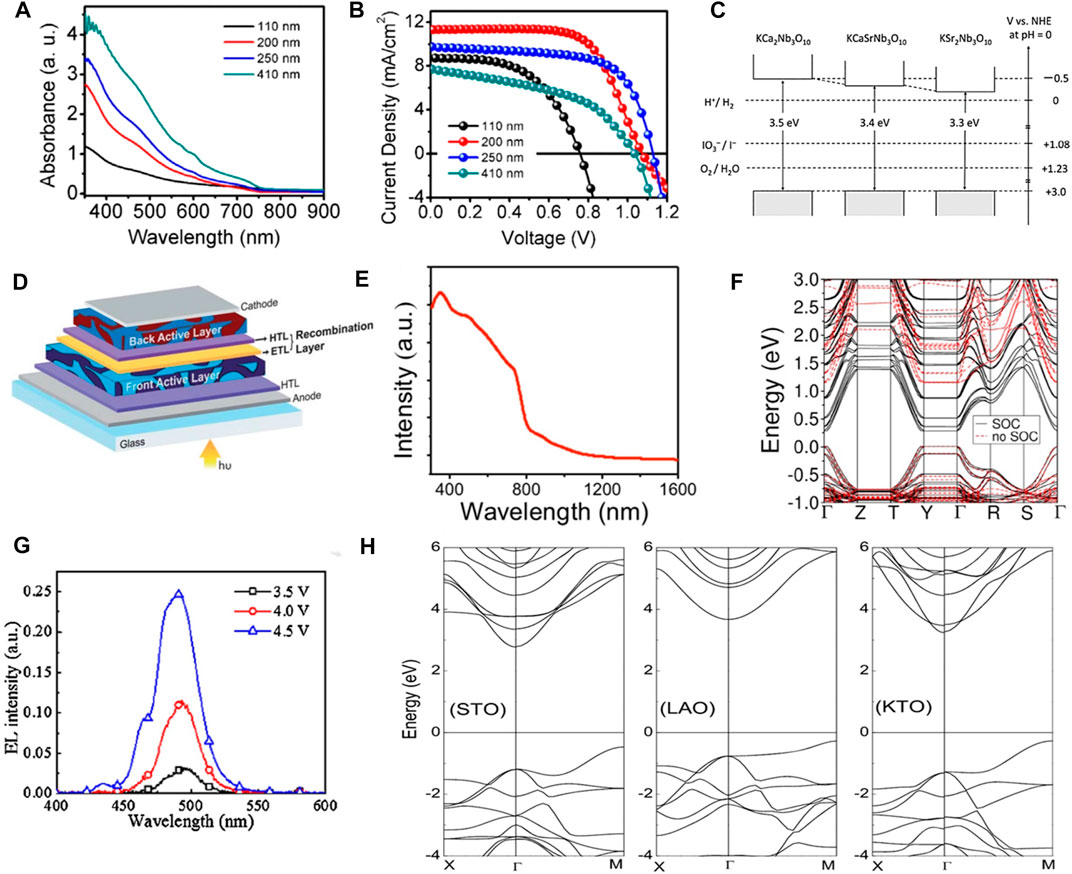
FIGURE 7. (A) UV-Vis absorption spectra of 2D Pb5 perovskite films. (B) J-V curves of Pb5 devices [adapted and modified from (Liu et al., 2017)]. (C) Schematic illustration of the band structures of restacked KCa2Nb3O10, KCaSrNb3O10, and KSr2Nb3O10 [adapted and modified from (Oshima et al., 2016]. (D) Device structure of tandem polymer solar cell [adapted and modified from Chang et al., 2012)]. (E) UV-Vis near-IR absorption spectrum of the 2D CH3NH3PbI3 perovskite nanosheets [adapted and modified from (Li et al., 2017)]. (F) Band structure of BA2MA4Pb5I16 with and without SOC [adapted and modified from (Stoumpos et al., 2017)]. (G) Electroluminescent spectra of PCPbB device at different applied voltages [adapted and modified from Cheng et al., 2017)]. (H) Band structures of STO-ML, LAO-ML, and KTO-ML [adapted and modified from (Xiao and Liu, 2021)].
The most recent advances in the 2D organic-inorganic halide perovskites have become competitive materials in providing efficient solar energy. The stability and optimization of recent research in improvising the PSCs involves tuning of structures, composition, and defect passivation in perovskite absorbers, the device structure, and also the interface modifications (Tormann et al., 2016; Correa-Baena et al., 2017; Zheng et al., 2017, 2019; Zhang et al., 2020). After the first report of 2D perovskites as absorbers, the recent advancements have reached achieving ∼18% efficiency (Luo et al., 2019). One of the most recent studies of organic-inorganic hybrid perovskite was done with 2D hybrid lead bromides, (C7H18N2)PbBr4, and (C9H22N2)PbBr4; their possible use in the optoelectronic field was discussed briefly. Their optical bandgap lies in between 2.76 and 2.78 eV, respectively, for (C7H18N2)PbBr4 and (C9H22N2)PbBr4. Along with it, we observe broad photoluminescent spectra that originate from free and self-trapped excitons (Deng et al., 2020). The exciton energy levels were controlled through chain length variations which influenced the optical properties in the material. In another study, the high tunability in the state-of-the-art hybrid Ruddlesden-Popper perovskites (RPPs) was discussed (Gan et al., 2021). As compared to their bulk counterpart, the 2D layered RPPs showed improved environmental stability on external factors affecting the device like light, stress, and humidity (Tsai et al., 2016). This was attributed to the absence of ion migration in 2D RPPs and hence improving the retention capacity and better performance in optical devices.
2D Metal-Organic Framework Nanosheets
Metal-organic frameworks (MOFs) are multifunctional materials that can be structurally designed. Fabricated 2D MOFs offer a large number of applications in the field of sensing, energy storage, electronic device fabrication, and many more. Materials inducing photochromism have been widely used in optoelectronics, data storage, transmission materials, and many more (Natali and Giordani, 2012; Irie et al., 2014). Photochromism allows the modulation in materials with light as an external stimulus. Studies of exfoliated MONs have been thoroughly explored for this property recently. Figure 8A depicts UV-Vis absorption spectra of Cd-DP, Zn-DA, and Cd-TA with a peak at 605 nm, and for Cd-TP, it is 615 nm. Figure 8B shows an SEM image of CdCl2 treated with pyridyl (Cd-DP) (Mukhopadhyay et al., 2018). Luminescence property was studied for free-standing flakes of [Cu (µ-pym2S2) (µ-Cl)]n, and bands were observed at 580, 615, and 650 nm (Figure 8C); the similarities and differences between the flakes and bulk samples are observed. A slightly larger intensity was observed in the spectrum of free-standing flakes, and they do not arise from flake–substrate interactions concerning Si/SiO2 substrates sample deposition (Hermosa et al., 2015). Ordered networks of chromophores achieved artificial and natural light-harvesting arrays for energy transfer. Some MOFs mimic this property in order to provide efficient light to electrical conversion. Figure 8D shows excitation resulting in emission at 596 nm for bodipy-porphyrin-based MOF (BOB) and bodipy and a dibrominated strut (BOP) showed no emission at 596 nm but at 667 nm. For the same samples, efficient energy transfer was observed in BOP MOF (Figure 8E) (Lee et al., 2011). Tetrakis (4-carboxyphenyl)porphyrin (TCPP) based MONs have been used as light-harvesting functional materials (Zhang and Lin, 2014). 2D MOFs have also been used as fluorescent biosensors in order to detect DNA, m-RNA, and other optical and electrochemical sensing units (Zhao et al., 2015; Zhao et al., 2018 M.).
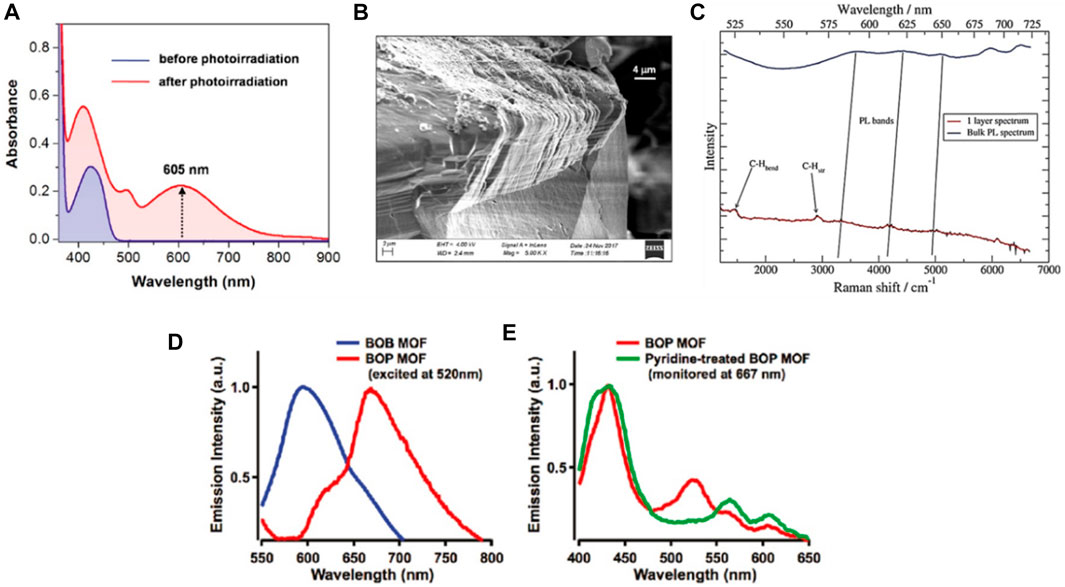
FIGURE 8. (A) UV-visible absorption spectra of Cd-DP. (B) SEM images of Cd-DP [adapted and modified from (Mukhopadhyay et al., 2018)]. (C) Raman and photoluminescence spectra of [Cu(μ-pym2S2) (μ-Cl)]n nMeOH [adapted and modified from (Hermosa et al., 2015)]. (D) PL spectra of BOB and BOP MOFs and (E) PLE spectra of BOP and pyridine-treated BOP MOF [adapted and modified from (Lee et al., 2011)].
2D Heterostructures for Optical Devices
The interfaces of the 2D material and other 2D-2D heterostructures play an important role in optical device fabrication. A few of the important studies pertaining to the same have been discussed in this section. 2D materials with heterostructure interfaces have been quite popular as they dominate by surface chemistry. They offer a wide range of tunability and unique properties to work with. Most 2D materials are integral parts of bulk layered vdW crystals. This atomically thin nature of 2D materials offers opportunities for building functional heterostructures, making it ideal for wearable electronics and other optoelectronic devices (Liu and Hersam, 2018). Studies on geometrical distortions and other surface mechanisms in 2D materials have a direct impact on the heterostructure composite formations and the 2D material offers better performance than those compared to its bulk. These 2D heterostructures find wide applications in optical based electronic systems because of generated interlayer excitons and flexible band tuning. They also offer a wide range of spectrum of operation from UV to near-infrared (NIR). These multi-structures alter the device performances to a great extent (Deng et al., 2019). There also exist studies on 2D metal-semiconductor heterostructure interfaces as 2D metallic materials have a wider range of work functions (Tan J. et al., 2021). A photodetector achieved ultrahigh responses up to 2600 AW−1 and specific detectivity up to 1.1 × 10⁻¹³ Jones over a wide spectrum (Li et al., 2019).
Future Perspectives and Conclusion
The optical properties of 2D material have been discussed here. In this review, we have discussed the advancements in the optical field. Graphene shows excellent optoelectronic properties in various areas. The review shows that while the 2D TMDs, MO, and MXens can be a part of the endless amount of work in optics, several modifications are needed for the enhancement of optoelectronics applications in modern electronics.
Making heterojunctions is another way that can be explored with 2D materials. To fine-tune the optical properties of the 2D materials, the formation of heterojunction provides excellent flexibility. Several methods have been used to make heterojunctions. For enhancing the device performance, making an interface with continuous band alignment, optimizing the carrier numbers, etc., can be employed. The 3D printing technology can be utilized to build 2D materials optoelectronics circuits to tune the properties of the device. The heterojunction of 2D materials will be formed layer by layer using 3D printing. For fabrication of stacked heterostructure of few atomic thicknesses of each layer, 3D printing method, CVD, epitaxial growth technique, and so forth can be done. These kinds of vertically stacked heterostructure can be a potential candidate for functional integrated optical devices such as photovoltaic cells, phototransistors, photodetector, LEDs, and optical sensors. Also, the high sensitivity to the environmental changes of 2D materials makes them promising candidates for biosensing applications. Modification of electronic structure is a useful technique that can improve the optoelectronic properties of the 2D materials. To improve the performance of the 2D-2D heterojunction in optoelectronic devices, electron-hole transport phenomena will be control by engineering the interfacial band structure. The interfacial charge and energy transfer play an essential role for optoelectronic devices. Therefore, optimization of several parameters, such as bandgap offset at the interface, thickness of spacer, laser excitation power, charge separation, and transport rate, is very important for future optoelectronics devices using 2D materials. Generally, 2D materials also show high electron mobility which increases the efficiency of the photo carriers. Therefore, during the fabrication of heterojunction devices, the selection of appropriate 2D materials is very important. Additionally, to modify the device structures, 3D printing technology is one of the promising approaches. In the case of 3D printed based hybrid optical devices, tuning the layer number, charge transport modification, alloying, and so forth of these 2D materials, we will improve the efficiency of the fabricated heterojunction. We hope the present work will contribute to further works on these exciting materials.
In this review, we have summarized the optical properties of 2D layered materials. We have discussed the optical properties and optoelectronic applications of several 2D materials like graphene, h-BN, TMDs, BP, MXens, and perovskites. In addition to these, we have also summarized the emission properties under different environmental conditions in the long-wavelength range. The origin of this tunable emission property of these atomically thin materials has been discussed thoroughly. Additionally, technological advancement with different innovations, such as generation and tuning of surface defects in a 2D lattice and making of heterostructures with 2D material, are discussed. The nonlinear optical properties of these 2D materials are also discussed in detail due to their potential applications for next-generation devices with excellent optical sensitivity, optical switching, and so forth. The optimization of device parameters is also discussed elaborately in this review. Along with experimental results, theoretical modeling of various 2D materials is also summarized. Therefore, this review presents the different methodological basis for developing 2D optical materials and a wide range of fabricating technologies. It will expand the optical application of these materials in the technology and production of optoelectronic devices. This greatly increases the ability of scientists to investigate the relationship between structural characteristics and physical properties of 2D optical materials.
Author Contributions
PK: visualization, investigation, formal analysis, and writing—original draft; CG: visualization, resources, software, data curation, and repetition writing—review and editing; CST: supervision, project administration, and funding acquisition.
Conflict of Interest
The authors declare that the research was conducted in the absence of any commercial or financial relationships that could be construed as a potential conflict of interest.
Publisher’s Note
All claims expressed in this article are solely those of the authors and do not necessarily represent those of their affiliated organizations, or those of the publisher, the editors and the reviewers. Any product that may be evaluated in this article, or claim that may be made by its manufacturer, is not guaranteed or endorsed by the publisher.
Acknowledgments
PK and CST acknowledge AOARD (Asian Office of Aerospace Research and Development) grant no. FA2386-19-1-4039. CST acknowledges Ramanujan fellowship and core research grant of SERB, India. CST acknowledges the funding received from STARS project by MHRD, India.
References
Abdelrazik, A. S., Tan, K. H., Aslfattahi, N., Arifutzzaman, A., Saidur, R., and Al-Sulaiman, F. A. (2020a). Optical, Stability and Energy Performance of Water-Based MXene Nanofluids in Hybrid PV/thermal Solar Systems. Solar Energy 204, 32–47. doi:10.1016/j.solener.2020.04.063
Abdelrazik, A. S., Tan, K. H., Aslfattahi, N., Saidur, R., and Al‐Sulaiman, F. A. (2020b). Optical Properties and Stability of Water‐based Nanofluids Mixed with Reduced Graphene Oxide Decorated with Silver and Energy Performance Investigation in Hybrid Photovoltaic/thermal Solar Systems. Int. J. Energ. Res. 44, 11487–11508. doi:10.1002/er.5770
Abed Al- Abbas, S. S., Muhsin, M. K., and Jappor, H. R. (2018). Tunable Optical and Electronic Properties of Gallium telluride Monolayer for Photovoltaic Absorbers and Ultraviolet Detectors. Chem. Phys. Lett. 713, 46–51. doi:10.1016/j.cplett.2018.10.020
Aslfattahi, N., Saidur, R., Arifutzzaman, A., Sadri, R., Bimbo, N., Sabri, M. F. M., et al. (2020a). Experimental Investigation of Energy Storage Properties and thermal Conductivity of a Novel Organic Phase Change material/MXene as A New Class of Nanocomposites. J. Energ. Storage 27, 101115. doi:10.1016/j.est.2019.101115
Aslfattahi, N., Samylingam, L., Abdelrazik, A. S., Arifutzzaman, A., and Saidur, R. (2020b). MXene Based New Class of Silicone Oil Nanofluids for the Performance Improvement of Concentrated Photovoltaic thermal Collector. Solar Energ. Mater. Solar Cell 211, 110526. doi:10.1016/j.solmat.2020.110526
Behura, S. K., Wang, C., Wen, Y., and Berry, V. (2019). Graphene‐Semiconductor Heterojunction Sheds Light on Emerging Photovoltaics. Nature Photonics 13, 312–318.
Cadiz, F., Courtade, E., Robert, C., Wang, G., Shen, Y., Cai, H., et al. (2017). Excitonic Linewidth Approaching the Homogeneous Limit in MoS2-Based van der Waals Heterostructures. Physical Review X 7, 021026. doi:10.1103/PhysRevX.7.021026
Cao, T., Li, Z., Qiu, D. Y., and Louie, S. G. (2016). Gate Switchable Transport and Optical Anisotropy in 90° Twisted Bilayer Black Phosphorus. Nano Lett. 16, 5542–5546. doi:10.1021/acs.nanolett.6b02084
Chang, L., Holmes, M. A., Waller, M., Osterloh, F. E., and Moulé, A. J. (2012). Calcium Niobate Nanosheets as a Novel Electron Transport Material for Solution-Processed Multi-junction Polymer Solar Cells. J. Mater. Chem. 22, 20443–20450. doi:10.1039/c2jm33351a
Chaudhuri, K., Alhabeb, M., Wang, Z., Shalaev, V. M., Gogotsi, Y., and Boltasseva, A. (2018). Highly Broadband Absorber Using Plasmonic Titanium Carbide (MXene). ACS Photon. 5, 1115–1122. doi:10.1021/acsphotonics.7b01439
Chen, H., Liu, T., Su, Z., Shang, L., and Wei, G. (2018). 2D Transition Metal Dichalcogenide Nanosheets for Photo/thermo-Based Tumor Imaging and Therapy. Nanoscale Horiz. 3, 74–89. doi:10.1039/c7nh00158d
Chen, K., Zhou, X., Cheng, X., Qiao, R., Cheng, Y., Liu, C., et al. (2019). Graphene Photonic crystal Fibre with strong and Tunable Light-Matter Interaction. Nat. Photon. 13, 754–759. doi:10.1038/s41566-019-0492-5
Cheng, L., Cao, Y., Ge, R., Wei, Y.-Q., Wang, N.-N., Wang, J.-P., et al. (2017). Sky-blue Perovskite Light-Emitting Diodes Based on Quasi-Two-Dimensional Layered Perovskites. Chin. Chem. Lett. 28, 29–31. doi:10.1016/j.cclet.2016.07.001
Chertopalov, S., and Mochalin, V. N. (2018). Environment-Sensitive Photoresponse of Spontaneously Partially Oxidized Ti3C2 MXene Thin Films. ACS Nano 12, 6109–6116. doi:10.1021/acsnano.8b02379
Compton, O. C., Carroll, E. C., Kim, J. Y., Larsen, D. S., and Osterloh, F. E. (2007). Calcium Niobate Semiconductor Nanosheets as Catalysts for Photochemical Hydrogen Evolution from Water. J. Phys. Chem. C 111, 14589–14592. doi:10.1021/jp0751155
Correa-Baena, J.-P., Saliba, M., Buonassisi, T., Grätzel, M., Abate, A., Tress, W., et al. (2017). Promises and Challenges of Perovskite Solar Cells. Science 358, 739–744. doi:10.1126/science.aam6323
Deng, C., Zhou, G., Chen, D., Zhao, J., Wang, Y., and Liu, Q. (2020). Broadband Photoluminescence in 2D Organic-Inorganic Hybrid Perovskites: (C7H18N2)PbBr4 and (C9H22N2)PbBr4. J. Phys. Chem. Lett. 11, 2934–2940. doi:10.1021/acs.jpclett.0c00578
Deng, P., Yang, J., Li, S., Fan, T.-E., Wu, H.-H., Mou, Y., et al. (2019). High Initial Reversible Capacity and Long Life of Ternary SnO2-Co-Carbon Nanocomposite Anodes for Lithium-Ion Batteries. Nano-micro Lett. 11, 1–13. doi:10.1007/s40820-019-0246-4
Eda, G., Yamaguchi, H., Voiry, D., Fujita, T., Chen, M., and Chhowalla, M. (2011). Photoluminescence from Chemically Exfoliated MoS2. Nano Lett. 11, 5111–5116. doi:10.1021/nl201874w
Fonseca, J. I., Tongay, S., Tongay, M., Tongay, A. R., Lin, A. J., Ko, C., et al. (2016). Bandgap Restructuring of the Layered Semiconductor Gallium Telluride in Air. Adv. Materials 28, 6465–6470. doi:10.1002/adma.201601151
Gan, X., Shiue, R.-J., Gao, Y., Meric, I., Heinz, T. F., Shepard, K., et al. (2013). Chip-integrated Ultrafast Graphene Photodetector with High Responsivity. Nat. Photon 7, 883–887. doi:10.1038/nphoton.2013.253
Gan, Z., Cheng, Y., Chen, W., Loh, K. P., Jia, B., and Wen, X. (2021). Photophysics of 2D Organic-Inorganic Hybrid Lead Halide Perovskites: Progress, Debates, and Challenges. Adv. Sci. 8, 2001843–2001918. doi:10.1002/advs.202001843
Grigorenko, A. N., Polini, M., and Novoselov, K. S. (2012). Graphene Plasmonics. Nat. Photon 6, 749–758. doi:10.1038/nphoton.2012.262
Guo, B., Xiao, Q. L., Wang, S. H., and Zhang, H. (2019). 2D Layered Materials: Synthesis, Nonlinear Optical Properties, and Device Applications. Laser Photon. Rev. 13, 1800327–1800346. doi:10.1002/lpor.201800327
Hantanasirisakul, K., Alhabeb, M., Lipatov, A., Maleski, K., Anasori, B., Salles, P., et al. (2019). Effects of Synthesis and Processing on Optoelectronic Properties of Titanium Carbonitride MXene. Chem. Mater. 31, 2941–2951. doi:10.1021/acs.chemmater.9b00401
Hermosa, C., Horrocks, B. R., Martínez, J. I., Liscio, F., Gómez-Herrero, J., and Zamora, F. (2015). Mechanical and Optical Properties of Ultralarge Flakes of a Metal-Organic Framework with Molecular Thickness. Chem. Sci. 6, 2553–2558. doi:10.1039/c4sc03115f
Huang, J., Dong, N., Zhang, S., Sun, Z., Zhang, W., and Wang, J. (2017). Nonlinear Absorption Induced Transparency and Optical Limiting of Black Phosphorus Nanosheets. ACS Photon. 4, 3063–3070. doi:10.1021/acsphotonics.7b00598
Huang, S., Tatsumi, Y., Ling, X., Guo, H., Wang, Z., Watson, G., et al. (2016). In-Plane Optical Anisotropy of Layered Gallium Telluride. ACS Nano 10, 8964–8972. doi:10.1021/acsnano.6b05002
Huang, Z.-P., Ma, B., Wang, H., Li, N., Liu, R.-T., Zhang, Z.-Q., et al. (2020). In Situ Growth of 3D/2D (CsPbBr3/CsPb2Br5) Perovskite Heterojunctions toward Optoelectronic Devices. J. Phys. Chem. Lett. 11, 6007–6015. doi:10.1021/acs.jpclett.0c01757
Hwang, M. T., Heiranian, M., Kim, Y., You, S., Leem, J., Taqieddin, A., et al. (2020). Ultrasensitive Detection of Nucleic Acids Using Deformed Graphene Channel Field Effect Biosensors. Nat. Commun. 11. doi:10.1038/s41467-020-15330-9
Irie, M., Fukaminato, T., Matsuda, K., and Kobatake, S. (2014). Photochromism of Diarylethene Molecules and Crystals: Memories, Switches, and Actuators. Chem. Rev. 114, 12174–12277. doi:10.1021/cr500249p
Jia, Y., Zhao, H., Guo, Q., Wang, X., Wang, H., and Xia, F. (2015). Tunable Plasmon-Phonon Polaritons in Layered Graphene-Hexagonal Boron Nitride Heterostructures. ACS Photon. 2, 907–912. doi:10.1021/acsphotonics.5b00099
Jiang, T., Kravtsov, V., Tokman, M., Belyanin, A., and Raschke, M. B. (2019). Ultrafast Coherent Nonlinear Nanooptics and Nanoimaging of Graphene. Nat. Nanotechnol. 14, 838–843. doi:10.1038/s41565-019-0515-x
Jo, S.-H., Kang, D.-H., Shim, J., Jeon, J., and Jeon, M. B. (2016). A High-Performance WSe2/h-BN Photodetector Using a Triphenylphosphine (PPh3)-Based n-Doping Technique. Adv. Materials 28, 4824–4831. doi:10.1002/adma.201600032
Johnson, V. L., Anilao, A., and Koski, K. J. (2019). Pressure-dependent Phase Transition of 2D Layered Silicon telluride (Si2Te3) and Manganese Intercalated Silicon telluride. Nano Res. 12, 2373–2377. doi:10.1007/s12274-019-2387-7
Kang, J., Sangwan, V. K., Lee, H. S., Liu, X., and Hersam, M. C. (2018). Solution-Processed Layered Gallium Telluride Thin-Film Photodetectors. ACS Photonics 5, 3996–4002. doi:10.1021/acsphotonics.8b01066
Kelly, K. L., Coronado, E., Zhao, L. L., and Schatz, G. C. (2003). The Optical Properties of Metal Nanoparticles: The Influence of Size, Shape, and Dielectric Environment. J. Phys. Chem. B 107, 668–677. doi:10.1021/jp026731y
Kim, Y. D., Kim, H., Cho, Y., Ryoo, J. H., Park, C.-H., Kim, P., et al. (2015). Bright Visible Light Emission from Graphene. Nat. Nanotech. 10, 676–681. doi:10.1038/nnano.2015.118
Kobayashi, Y., Sasaki, S., Mori, S., Hibino, H., Liu, Z., Watanabe, K., et al. (2015). Growth and Optical Properties of High-Quality Monolayer WS2 on Graphite. ACS Nano 9, 4056–4063. doi:10.1021/acsnano.5b00103
Konstantatos, G., Badioli, M., Gaudreau, L., Osmond, J., Bernechea, M., Garcia de Arquer, F. P., et al. (2012). Hybrid Graphene‐Quantum Dot Phototransistors With Ultrahigh Gain. Nat. Nanotechnol. 7, 363–368. doi:10.1038/nnano.2012.60
Kravets, V. G., Wu, F., Auton, G. H., Yu, T., Imaizumi, S., and Grigorenko, A. N. (2019). Measurements of Electrically Tunable Refractive index of MoS2 Monolayer and its Usage in Optical Modulators. Npj 2d Mater. Appl. 3, 1–10. doi:10.1038/s41699-019-0119-1
Kumar, A., Low, T., Fung, K. H., Avouris, P., and Fang, N. X. (2015). Tunable Light-Matter Interaction and the Role of Hyperbolicity in Graphene-Hbn System. Nano Lett. 15, 3172–3180. doi:10.1021/acs.nanolett.5b01191
Kumbhakar, P., Biswas, S., Pandey, P., Tiwary, C. S., and Kumbhakar, P. (2019). Tailoring of Structural and Photoluminescence Emissions by Mn and Cu Co-doping in 2D Nanostructures of ZnS for the Visualization of Latent Fingerprints and Generation of white Light. Nanoscale 11, 2017–2026. doi:10.1039/c8nr09074b
Latini, S., Winther, K. T., Olsen, T., and Thygesen, K. S. (2017). Interlayer Excitons and Band Alignment in MoS2/hBN/WSe2 van der Waals Heterostructures. Nano Lett. 17, 938–945. doi:10.1021/acs.nanolett.6b04275
Lee, C. Y., Farha, O. K., Hong, B. J., Sarjeant, A. A., Nguyen, S. T., and Hupp, J. T. (2011). Light-harvesting Metal-Organic Frameworks (MOFs): Efficient Strut-To-Strut Energy Transfer in Bodipy and Porphyrin-Based MOFs. J. Am. Chem. Soc. 133, 15858–15861. doi:10.1021/ja206029a
Li, A., Chen, Q., Wang, P., Gan, Y., Qi, T., Wang, P., et al. (2019). Ultrahigh‐Sensitive Broadband Photodetectors Based on Dielectric Shielded MoTe 2/Graphene/SnS 2 P-G-N Junctions. Adv. Mater. 31, 1805656–1805659. doi:10.1002/adma.201805656
Li, B.-W., Osada, M., Ozawa, T. C., Ebina, Y., Akatsuka, K., Ma, R., et al. (2010). Engineered Interfaces of Artificial Perovskite Oxide Superlattices via Nanosheet Deposition Process. ACS Nano 4, 6673–6680. doi:10.1021/nn102144s
Li, P., Chen, Y., Yang, T., Wang, Z., Lin, H., Xu, Y., et al. (2017). Two-Dimensional CH3NH3PbI3 Perovskite Nanosheets for Ultrafast Pulsed Fiber Lasers. ACS Appl. Mater. Inter. 9, 12759–12765. doi:10.1021/acsami.7b01709
Liu, B., Soe, C. M. M., Stoumpos, C. C., Nie, W., Tsai, H., Lim, K., et al. (2017). Optical Properties and Modeling of 2D Perovskite Solar Cells. Sol. RRL 1, 1700062–1700068. doi:10.1002/solr.201700062
Liu, M., Yin, X., Ulin-Avila, E., Geng, B., Zentgraf, T., Ju, L., et al. (2011). A Graphene-Based Broadband Optical Modulator. Nature 474, 64–67. doi:10.1038/nature10067
Liu, W., Liu, M., Liu, X., Wang, X., Deng, H. X., Lei, M., et al. (2020). Recent Advances of 2D Materials in Nonlinear Photonics and Fiber Lasers. Adv. Opt. Mater. 8, 1901631. doi:10.1002/adom.201901631
Liu, X., and Hersam, M. C. (2018). Interface Characterization and Control of 2D Materials and Heterostructures. Adv. Mater. 30, 1801586. doi:10.1002/adma.201801586
Lorchat, E., López, L. E. P., Robert, C., Lagarde, D., Froehlicher, G., Taniguchi, T., et al. (2020). Filtering the Photoluminescence Spectra of Atomically Thin Semiconductors with Graphene. Nat. Nanotechnol. 15, 283–288. doi:10.1038/s41565-020-0644-2
Lu, J., Yang, J., Carvalho, A., Liu, H., Lu, Y., and Sow, C. H. (2016). Light-Matter Interactions in Phosphorene. Acc. Chem. Res. 49, 1806–1815. doi:10.1021/acs.accounts.6b00266
Luo, T., Zhang, Y., Xu, Z., Niu, T., Wen, J., Lu, J., et al. (2019). Compositional Control in 2D Perovskites with Alternating Cations in the Interlayer Space for Photovoltaics with Efficiency over 18. Adv. Mater. 31, e1903848–8. doi:10.1002/adma.201903848
Lyu, B., Li, H., Jiang, L., Shan, W., Hu, C., Deng, A., et al. (2019). Phonon Polariton-Assisted Infrared Nanoimaging of Local Strain in Hexagonal Boron Nitride. Nano Lett. 19, 1982–1989. doi:10.1021/acs.nanolett.8b05166
Ma, Q., Ren, G., Xu, K., and Ou, J. Z. (2021). Tunable Optical Properties of 2D Materials and Their Applications. Adv. Opt. Mater. 9, 2001313–2001326. doi:10.1002/adom.202001313
Mak, K. F., and Shan, J. (2016). Photonics and Optoelectronics of 2D Semiconductor Transition Metal Dichalcogenides. Nat. Photon 10, 216–226. doi:10.1038/nphoton.2015.282
Meng, X., Wang, X., Cheng, Z., Tian, N., Lang, M. C., Yan, W., et al. (2018). Photoluminescence Lifetime of Black Phosphorus Nanoparticles and Their Applications in Live Cell Imaging. ACS Appl. Mater. Inter. 10, 31136–31145. doi:10.1021/acsami.8b11648
Mudd, G. W., Svatek, S. A., Ren, T., Patanè, A., Makarovsky, O., Eaves, L., et al. (2013). Tuning the Bandgap of Exfoliated InSe Nanosheets by Quantum Confinement. Adv. Mater. 25, 5714–5718. doi:10.1002/adma.201302616
Mukhopadhyay, A., Maka, V. K., Savitha, G., and Moorthy, J. N. (2018). Photochromic 2D Metal-Organic Framework Nanosheets (MONs): Design, Synthesis, and Functional Mon-Ormosil Composite. Chem 4, 1059–1079. doi:10.1016/j.chempr.2018.03.013
Natali, M., and Giordani, S. (2012). Molecular Switches as Photocontrollable “Smart” Receptors. Chem. Soc. Rev. 41, 4010–4029. doi:10.1039/c2cs35015g
Ni, G. X., Wang, L., Goldflam, M. D., Wagner, M., Fei, Z., McLeod, A. S., et al. (2016). Ultrafast Optical Switching of Infrared Plasmon Polaritons in High-Mobility Graphene. Nat. Photon. 10, 244–247. doi:10.1038/nphoton.2016.45
Noh, H.-J., Im, Y.-K., Yu, S.-Y., Seo, J.-M., Mahmood, J., Yildirim, T., et al. (2020). Vertical Two-Dimensional Layered Fused Aromatic Ladder Structure. Nat. Commun. 11, 1–8. doi:10.1038/s41467-020-16006-0
Noumbé, U. N., Noumbé, C., Livache, C., Chu, A., and Majjad, H. (2020). Reconfigurable 2D/0D p–n Graphene/HgTe Nanocrystal Heterostructure for Infrared Detection. ACS Nano 14, 4567–4576. doi:10.1021/acsnano.0c00103
Ono, M., Hata, M., Tsunekawa, M., Nozaki, K., Sumikura, H., Chiba, H., et al. (2020). Ultrafast and Energy-Efficient All-Optical Switching with Graphene-Loaded Deep-Subwavelength Plasmonic Waveguides. Nat. Photon. 14, 37–43. doi:10.1038/s41566-019-0547-7
Opoku, F., Govender, K. K., van Sittert, C. G. C. E., and Govender, P. P. (2017). Enhancing Charge Separation and Photocatalytic Activity of Cubic SrTiO3with Perovskite-type Materials MTaO3(M=Na, K) for Environmental Remediation: A First-Principles Study. ChemistrySelect 2, 6304–6316. doi:10.1002/slct.201700886
Oshima, T., Eguchi, M., and Maeda, K. (2016). Photocatalytic Water Oxidation over Metal Oxide Nanosheets Having a Three-Layer Perovskite Structure. ChemSusChem 9, 396–402. doi:10.1002/cssc.201501237
Perumal Veeramalai, C., Yang, S., Wei, J., Sulaman, M., Zhi, R., Saleem, M. I., et al. (2020). Porous Single-Wall Carbon Nanotube Templates Decorated with All-Inorganic Perovskite Nanocrystals for Ultraflexible Photodetectors. ACS Appl. Nano Mater. 3, 459–467. doi:10.1021/acsanm.9b02051
Pramanik, A., Biswas, S., Tiwary, C. S., Sarkar, R., and Kumbhakar, P. (2018). Colloidal N-Doped Graphene Quantum Dots with Tailored Luminescent Downshifting and Detection of UVA Radiation with Enhanced Responsivity. ACS Omega 3, 16260–16270. doi:10.1021/acsomega.8b02473
Qiao, J., Kong, X., Hu, Z.-X., Yang, F., and Ji, W. (2014). High-mobility Transport Anisotropy and Linear Dichroism in Few-Layer Black Phosphorus. Nat. Commun. 5, 1–7. doi:10.1038/ncomms5475
Qiao, M., Chen, Y., Wang, Y., and Li, Y. (2018). The Germanium telluride Monolayer: A Two Dimensional Semiconductor with High Carrier Mobility for Photocatalytic Water Splitting. J. Mater. Chem. A. 6, 4119–4125. doi:10.1039/c7ta10360c
Qiu, D. Y., Da Jornada, F. H., and Louie, S. G. (2017). Environmental Screening Effects in 2D Materials: Renormalization of the Bandgap, Electronic Structure, and Optical Spectra of Few-Layer Black Phosphorus. Nano Lett. 17, 4706–4712. doi:10.1021/acs.nanolett.7b01365
Quereda, J., San-Jose, P., Parente, V., Vaquero-Garzon, L., Molina-Mendoza, A. J., Agraït, N., et al. (2016). Strong Modulation of Optical Properties in Black Phosphorus through Strain-Engineered Rippling. Nano Lett. 16, 2931–2937. doi:10.1021/acs.nanolett.5b04670
Samylingam, L., Aslfattahi, N., Saidur, R., Yahya, S. M., Afzal, A., Arifutzzaman, A., et al. (2020). Thermal and Energy Performance Improvement of Hybrid PV/T System by Using Olein palm Oil with MXene as a New Class of Heat Transfer Fluid. Solar Energ. Mater. Solar Cell 218, 110754. doi:10.1016/j.solmat.2020.110754
Sarycheva, A., Makaryan, T., Maleski, K., Satheeshkumar, E., Melikyan, A., Minassian, H., et al. (2017). Two-Dimensional Titanium Carbide (MXene) as Surface-Enhanced Raman Scattering Substrate. J. Phys. Chem. C 121, 19983–19988. doi:10.1021/acs.jpcc.7b08180
Siddique, S., Gowda, C. C., Tromer, R., Demiss, S., Gautam, A. R. S., Femi, O. E., et al. (2021). Scalable Synthesis of Atomically Thin Gallium Telluride Nanosheets for Supercapacitor Applications. ACS Appl. Nano Mater. 4, 4829–4838. doi:10.1021/acsanm.1c00428
Sriram, P., Wen, Y.-P., Manikandan, A., Hsu, K.-C., Tang, S.-Y., Hsu, B.-W., et al. (2020). Enhancing Quantum Yield in Strained MoS2 Bilayers by Morphology-Controlled Plasmonic Nanostructures toward Superior Photodetectors. Chem. Mater. 32, 2242–2252. doi:10.1021/acs.chemmater.9b02886
Stanciu, S. G., Tranca, D. E., Pastorino, L., Boi, S., Song, Y. M., Yoo, Y. J., et al. (2020). Characterization of Nanomaterials by Locally Determining Their Complex Permittivity with Scattering-type Scanning Near-Field Optical Microscopy. ACS Appl. Nano Mater. 3, 1250–1262. doi:10.1021/acsanm.9b02019
Stoumpos, C. C., Soe, C. M. M., Tsai, H., Nie, W., Blancon, J.-C., Cao, D. H., et al. (2017). High Members of the 2D Ruddlesden-Popper Halide Perovskites: Synthesis, Optical Properties, and Solar Cells of (CH3(CH2)3NH3)2(CH3NH3)4Pb5I16. Chem 2, 427–440. doi:10.1016/j.chempr.2017.02.004
Sun, J., Wang, Y., Guo, S., Wan, B., Dong, L., Gu, Y., et al. (2020). Lateral 2D WSe2 p–n Homojunction Formed by Efficient Charge-Carrier-Type Modulation for High-Performance Optoelectronics. Adv. Materials 32, 1906499. doi:10.1002/adma.201906499
Sun, Y., Fujisawa, K., Lin, Z., Lei, Y., Mondschein, J. S., Terrones, M., et al. (2017). Low-Temperature Solution Synthesis of Transition Metal Dichalcogenide Alloys with Tunable Optical Properties. J. Am. Chem. Soc. 139, 11096–11105. doi:10.1021/jacs.7b04443
Sun, Z., Martinez, A., and Wang, F. (2016). Optical Modulators with 2D Layered Materials. Nat. Photon 10, 227–238. doi:10.1038/nphoton.2016.15
Synnatschke, K., Cieslik, P. A., Harvey, A., Castellanos-Gomez, A., Tian, T., Shih, C.-J., et al. (2019). Length- and Thickness-Dependent Optical Response of Liquid-Exfoliated Transition Metal Dichalcogenides. Chem. Mater. 31, 10049–10062. doi:10.1021/acs.chemmater.9b02905
Szydłowska, B. M., Tywoniuk, B., and Blau, W. J. (2018). Size-Dependent Nonlinear Optical Response of Black Phosphorus Liquid Phase Exfoliated Nanosheets in Nanosecond Regime. ACS Photon. 5, 3608–3612. doi:10.1021/acsphotonics.8b00469
Tan, J., Li, S., Liu, B., and Cheng, H.-M. (2021a). Structure, Preparation, and Applications of 2D Material‐Based Metal-Semiconductor Heterostructures. Small Structures 2, 2000093. doi:10.1002/sstr.202000093
Tan, K. H., Samylingam, L., Aslfattahi, N., Saidur, R., and Kadirgama, K. (2021b). Optical and Conductivity Studies of Polyvinyl Alcohol-MXene (PVA-MXene) Nanocomposite Thin Films for Electronic Applications. Opt. Laser Technol. 136, 106772. doi:10.1016/j.optlastec.2020.106772
Tan, T., Jiang, X., Wang, C., Yao, B., and Zhang, H. (2020). 2D Material Optoelectronics for Information Functional Device Applications: Status and Challenges. Adv. Sci. 7, 2000058. doi:10.1002/advs.202000058
Tormann, T., Wiemer, S., Enescu, B., Hiramatsu, Y., Obara, K., Hardebeck, J. L., et al. (2016). That Generally Depends on the Asperity Size and Stress Drop and on the Resistance of the Matrix. This effective Radius R. Sci. 354, 92–96.
Tsai, H., Nie, W., Blancon, J.-C., Stoumpos, C. C., Asadpour, R., Harutyunyan, B., et al. (2016). High-efficiency Two-Dimensional Ruddlesden-Popper Perovskite Solar Cells. Nature 536, 312–316. doi:10.1038/nature18306
Venuthurumilli, P. K., Ye, P. D., and Xu, X. (2018). Plasmonic Resonance Enhanced Polarization-Sensitive Photodetection by Black Phosphorus in Near Infrared. ACS Nano 12, 4861–4867. doi:10.1021/acsnano.8b01660
Vikraman, D., Akbar, K., Hussain, S., Yoo, G., Jang, J.-Y., Chun, S.-H., et al. (2017). Direct Synthesis of Thickness-Tunable MoS2 Quantum Dot Thin Layers: Optical, Structural and Electrical Properties and Their Application to Hydrogen Evolution. Nano Energy 35, 101–114. doi:10.1016/j.nanoen.2017.03.031
Villegas, C. E. P., Rocha, A. R., and Marini, A. (2016). Anomalous Temperature Dependence of the Band Gap in Black Phosphorus. Nano Lett. 16, 5095–5101. doi:10.1021/acs.nanolett.6b02035
Virdi, K. S., Kauffmann, Y., Ziegler, C., Ganter, P., Blaha, P., Lotsch, B. V., et al. (2016). Band Gap Extraction from Individual Two-Dimensional Perovskite Nanosheets Using Valence Electron Energy Loss Spectroscopy. J. Phys. Chem. C 120, 11170–11179. doi:10.1021/acs.jpcc.6b00142
Wang, C., Zhang, G., Huang, S., Xie, Y., and Yan, H. (2020a). The Optical Properties and Plasmonics of Anisotropic 2D Materials. Adv. Opt. Mater. 8, 1900996. doi:10.1002/adom.201900996
Wang, Q., Guo, J., Ding, Z., Qi, D., Jiang, J., Wang, Z., et al. (2017). Fabry-Perot Cavity-Enhanced Optical Absorption in Ultrasensitive Tunable Photodiodes Based on Hybrid 2D Materials. Nano Lett. 17, 7593–7598. doi:10.1021/acs.nanolett.7b03579
Wang, Z., Li, F., Guo, J., Ma, C., Song, Y., He, Z., et al. (2020b). Facile Synthesis of 2D Tin Selenide for Near‐ and Mid‐Infrared Ultrafast Photonics Applications. Adv. Opt. Mater. 8, 1902183–1902211. doi:10.1002/adom.201902183
Xia, F., Wang, H., Xiao, D., Dubey, M., and Ramasubramaniam, A. (2014). Two-dimensional Material Nanophotonics. Nat. Photon 8, 899–907. doi:10.1038/nphoton.2014.271
Xiao, X., and Liu, B. (2021). Freestanding Perovskite Oxide Monolayers as Two-Dimensional Semiconductors. Nanotechnology 32, 145705. doi:10.1088/1361-6528/abd4a0
Ye, L., Li, H., Chen, Z., and Xu, J. (2016). Near-Infrared Photodetector Based on MoS2/Black Phosphorus Heterojunction. ACS Photon. 3, 692–699. doi:10.1021/acsphotonics.6b00079
Yin, Z., Li, H., Li, H., and Jiang, L. (2012). Single-Layer MoS2 Phototransistors. ACS Nano. 6, 74–80. doi:10.1021/nn2024557
Zahn, D., Hildebrandt, P.-N., Vasileiadis, T., Windsor, Y. W., Qi, Y., Seiler, H., et al. (2020). Anisotropic Nonequilibrium Lattice Dynamics of Black Phosphorus. Nano Lett. 20, 3728–3733. doi:10.1021/acs.nanolett.0c00734
Zhang, C., Ouyang, H., Miao, R., Sui, Y., Hao, H., Tang, Y., et al. (2019). Anisotropic Nonlinear Optical Properties of a SnSe Flake and a Novel Perspective for the Application of All‐Optical Switching. Adv. Opt. Mater. 7, 1900631–1900710. doi:10.1002/adom.201900631
Zhang, F., Lu, H., Tong, J., Berry, J. J., Beard, M. C., and Zhu, K. (2020). Advances in Two-Dimensional Organic-Inorganic Hybrid Perovskites. Energy Environ. Sci. 13, 1154–1186. doi:10.1039/c9ee03757h
Zhang, T., and Lin, W. (2014). Metal-organic Frameworks for Artificial Photosynthesis and Photocatalysis. Chem. Soc. Rev. 43, 5982–5993. doi:10.1039/c4cs00103f
Zhang, Y.-x., and Wang, Y.-h. (2017). Nonlinear Optical Properties of Metal Nanoparticles: A Review. RSC Adv. 7, 45129–45144. doi:10.1039/c7ra07551k
Zhao, K., Huang, F., Dai, C.-M., Li, W., Chen, S.-Y., Jiang, K., et al. (2018a). Temperature Dependence of Phonon Modes, Optical Constants, and Optical Band Gap in Two-Dimensional ReS2 Films. J. Phys. Chem. C 122, 29464–29469. doi:10.1021/acs.jpcc.8b08693
Zhao, M., Huang, Y., Peng, Y., Huang, Z., Ma, Q., and Zhang, H. (2018b). Two-dimensional Metal-Organic Framework Nanosheets: Synthesis and Applications. Chem. Soc. Rev. 47, 6267–6295. doi:10.1039/c8cs00268a
Zhao, M., Wang, Y., Ma, Q., Huang, Y., Zhang, X., Ping, J., et al. (2015). Ultrathin 2D Metal-Organic Framework Nanosheets. Adv. Mater. 27, 7372–7378. doi:10.1002/adma.201503648
Zheng, X., Chen, B., Dai, J., Fang, Y., Bai, Y., Lin, Y., et al. (2017). Defect Passivation in Hybrid Perovskite Solar Cells Using Quaternary Ammonium Halide Anions and Cations. Nat. Energ. 2, 1–9. doi:10.1038/nenergy.2017.102
Zheng, X., Troughton, J., Gasparini, N., Lin, Y., Wei, M., Hou, Y., et al. (2019). Quantum Dots Supply Bulk- and Surface-Passivation Agents for Efficient and Stable Perovskite Solar Cells. Joule 3, 1963–1976. doi:10.1016/j.joule.2019.05.005
Zhu, B., Wang, F., Li, P., Wang, C., and Gu, Y. (2018a). Surface Oxygen-Containing Defects of Graphene Nanosheets with Tunable Nonlinear Optical Absorption and Refraction. Phys. Chem. Chem. Phys. 20, 27105–27114. doi:10.1039/c8cp04940h
Keywords: 2D materials, optical property, nonlinear optical property, optoelectronic devices, absorption property
Citation: Kumbhakar P, Chowde Gowda C and Tiwary CS (2021) Advance Optical Properties and Emerging Applications of 2D Materials. Front. Mater. 8:721514. doi: 10.3389/fmats.2021.721514
Received: 07 June 2021; Accepted: 12 July 2021;
Published: 16 August 2021.
Edited by:
Weiliang Wang, Sun Yat-sen University, ChinaReviewed by:
Wanda Ziemkowska, Warsaw University of Technology, PolandHui Pan, University of Macau, China
Copyright © 2021 Kumbhakar, Chowde Gowda and Tiwary. This is an open-access article distributed under the terms of the Creative Commons Attribution License (CC BY). The use, distribution or reproduction in other forums is permitted, provided the original author(s) and the copyright owner(s) are credited and that the original publication in this journal is cited, in accordance with accepted academic practice. No use, distribution or reproduction is permitted which does not comply with these terms.
*Correspondence: Chandra Sekhar Tiwary, Y3N0Lmlpc2NAZ21haWwuY29t