 Meihong Huang1
 Pinghui Wu
 Yan Xu
- 1College of Transportation and Navigation, Quanzhou Normal University, Quanzhou, China
- 2School of Automation, Hangzhou Dianzi University, Hangzhou, China
- 3Fujian Provincial Key Laboratory for Advanced Micro-nano Photonics Technology and Devices, Quanzhou Normal University, Quanzhou, China
- 4College of Science, Zhejiang University of Technology, Hangzhou, China
- 5School of Science, Huzhou University, Huzhou, China
In recent years, as a renewable clean energy with many excellent characteristics, solar energy has been widely concerned. In this paper, we propose an ultra-broadband solar absorber based on metal tungsten and semiconductor GaAs structure. A multilayer metal semiconductor composite structure composed of W-Ti-GaAs three-layer films and GaAs gratings is proposed. The finite difference time domain method is used to simulate the performance of the proposed model. High efficiency surface plasmon resonance is excited by adjusting the geometric parameters, and the broadband absorption of up to 2,350 nm in 500–2850 nm is realized. The spectrum of the structure can be changed by adjusting the geometric parameters to meet different needs. The proposed absorber has good oblique incidence characteristics (0–60°) and high short-circuit current characteristics. The geometry of the absorber is clear, easy to manufacture, and has good photoelectric performance. It can realize solar energy collection, light heat conversion, high sensitive sensing and other functions.
Introduction
From the beginning of the 21st century, with the improvement of people’s living standards, there are more and more kinds of household appliances, and the demand for traditional fossil energy is also increasing, which is in contradiction with the characteristics of non-renewable resources. According to the existing data, if energy consumption can not be controlled before the end of this century, oil and natural gas energy will be exhausted, and coal reserves will be exhausted. With the decrease of these conventional non-renewable resources, how to effectively and reasonably use conventional energy, and develop and utilize new energy, especially renewable energy, is a major event in front of all mankind (Xiao et al., 2017; Tang et al., 2018; Cai et al., 2019; Sivák et al., 2020; Xie et al., 2020; Zhao et al., 2021).
Among all kinds of energy, as a renewable energy, solar energy is considered to be the most potential energy, because it is inexhaustible, reliable, less pollution and so on. As an important energy collection device, solar absorber has attracted more and more attention in recent years (Li et al., 2016; Chen et al., 2019a; Xiao et al., 2019; Li et al., 2020a; Roostaei et al., 2021). For an ideal absorber, it must have high efficiency light absorption and many other excellent physical properties, such as polarization stability and tunability (Li et al., 2020b; Wu et al., 2020; Yi et al., 2020; Chen et al., 2021a; Jiang et al., 2021a; Li et al., 2021a; Li et al., 2021b; Li-Ying et al., 2021; Zhou et al., 2021). However, the existing absorbers are generally limited by low temperature tolerance, low light absorption efficiency and materials (Chen et al., 2020; Chen et al., 2021b; Jiang et al., 2021b; Wang et al., 2021; Zhang et al., 2021). Therefore, a new type of broadband solar energy which can solve the above problems needs to be proposed. According to the actual situation of solar radiation in the range of 295–2,500 nm, the key to realize the efficient utilization of solar energy is to design a solar device which can match the band perfectly.
The research on broadband absorber has been carried out for many years in the world, and it has been used in solar cells, solar heating devices and photothermal converters (Liu et al., 2017; Keshavarz and Vafapour, 2019; Yu et al., 2020; Chen et al., 2021c; Su et al., 2021). For the design and improvement of broadband absorber, we should pay attention to the following aspects: the first is to select the appropriate material. Traditional precious metal materials such as gold and silver were used in the original broadband absorbers. However, due to its high cost and poor high temperature resistance, people began to pay attention to high melting point materials such as titanium nitride. They not only have high melting point, but also can excite effective plasmon. Secondly, the nanostructure design of broadband absorber is also very important. The multi-layer metal-insulator structure was first used, and then turned to simpler MIM or IMI nanostructures. Finally, the working area of broadband absorber, especially from ultraviolet to near-infrared, has been studied and improved. Efforts in these directions are to obtain ideal broadband absorbers for practical applications. For instance, Lei proposed an ultra-broadband absorber based on a thin metamaterial nanostructure composed of Ti-SiO2 cubes and Al bottom film. The proposed structure can achieve nearly perfect absorption with an average absorbance of 97% from 354 to 1,066 nm (Lei et al., 2018). Huang proposed a broadband absorber with near-unity absorption in the terahertz regime based on a target-patterned graphene sheet, the absorption bandwidth (more than 90%) is 1.57 THz with a central frequency of 1.83 THz under normal incidence (Huang et al., 2018). Although the characteristics of these absorbers are superior enough, their complex nanostructures and a variety of complex materials make the proposed absorbers difficult to apply. Therefore, an absorber with simple structure and excellent high absorptivity should be proposed.
In this paper, we propose a broadband solar absorber composed of W-Ti-GaAs three-layer thin film and GaAs grating, as shown in Figure 1. The proposed structure uses W metal as the substrate and GaAs semiconductor grating as the auxiliary structure. There is a layer of metal Ti between the w base and the GaAs film, and the top layer is a layer of ITO (refractive index is 2.0) film to reduce the reflection of the whole structure and improve the overall absorptivity. The electromagnetic field in different wavebands, the influence of structure parameters on the overall absorptivity and the distribution of solar absorption characteristics are simulated. The results show that its high absorptivity band width (>90%) can reach 2,350 nm, which matches the solar radiation range on the earth (about 295–2,500 nm), and can perfectly meet the actual work requirements.

FIGURE 1. (A) Schematic diagram of multilayer metal semiconductor structure (B) Side view.
Materials and Methods
In the simulation process, we define the grating period as p and its width as t. The thickness from ITO layer to GaAs layer is defined as h1-h4. The thickness of W base is much larger than the penetration depth of light, so that the light transmittance T of the whole structure is approximately zero. The TM polarized plane wave is used as the light source to project vertically into the structure. The periodic boundary condition is set in the x direction and the perfectly matched layer is set in the z direction. The specific parameters of all materials are from the material library of FDTD solution software (Cao et al., 2014; Deng et al., 2015; Deng et al., 2018; Xu et al., 2021). The light absorption is still calculated by the formula A = 1-T-R, where T represents transmission rate and R represents reflection (Zhang et al., 2015; Long et al., 2016; Lv et al., 2018).
The simulation results are shown in Figure 2. In order to verify the rationality of our proposed five-layer structure, we also calculate the absorption without top layer ITO (shown by the red line in the figure) and the absorption with only three layers of Ti-GaAs-W (shown by the blue line in the figure). It can be seen from the figure that when there are only three layers of film structure, the overall absorptivity is very low, and the highest absorptivity in the whole band is less than 70%. For the case of adding GaAs grating without ITO film, the absorption rate has been greatly improved compared with the three-layer film structure, but the absorptivity is less than 90% in 1,030–1,410 nm and 2000–2,450 nm, which is still unsatisfactory. In our final five-layer structure, the absorption is more than 90% in the wavelength range of about 500–2,850 nm, which is up to 2,350 nm. Through calculation, the average absorption is 95% in the bandwidth of 2,350 nm, which meets the requirements of practical application perfectly.
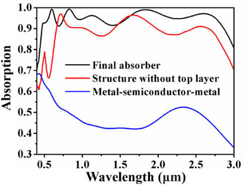
FIGURE 2. Absorption spectra of multilayer broadband absorber with different configurations.
Results and Discussion
First, we explore the influence of the main geometric parameters of the structure on the overall absorption, and the results are shown in Figure 3 Figure (a) shows the influence of the thickness of the top ITO film on the overall absorption. In the short wavelength range, the absorption changes greatly with the increase of the thickness, but at the long wavelength, it will gradually become better with the increase of the thickness and finally tend to remain unchanged. Considering the absorption of the whole band, we choose h1 = 80 nm as the optimal parameter. Figure (c) shows the effect of Ti film thickness on the structural absorptivity. When the thickness of Ti film is low, the absorptivity of the whole structure is poor, but with the increase of the thickness, it has a significant increase, and has a good absorption effect at h3 = 70–90 nm. The main reason is that the better impedance matching condition is met at this time. Figures (b) and (d) show the effects of the thickness of the two layers on the overall absorption. In figure (b), with the increase of h2, the long band absorption has been significantly improved. This is because the guided mode resonance of the grating layer is mainly related to its effective refractive index (Chen et al., 2013; Cai et al., 2014; Long et al., 2015), and the change of h2 will significantly change the effective refractive index of the waveguide layer. In figure (d), with the increase of the thickness, the absorption in the long band decreases gradually, while the absorption in the short band is almost unchanged. This is because the change of the film thickness will cause a weak change in the number of dielectric cavities.
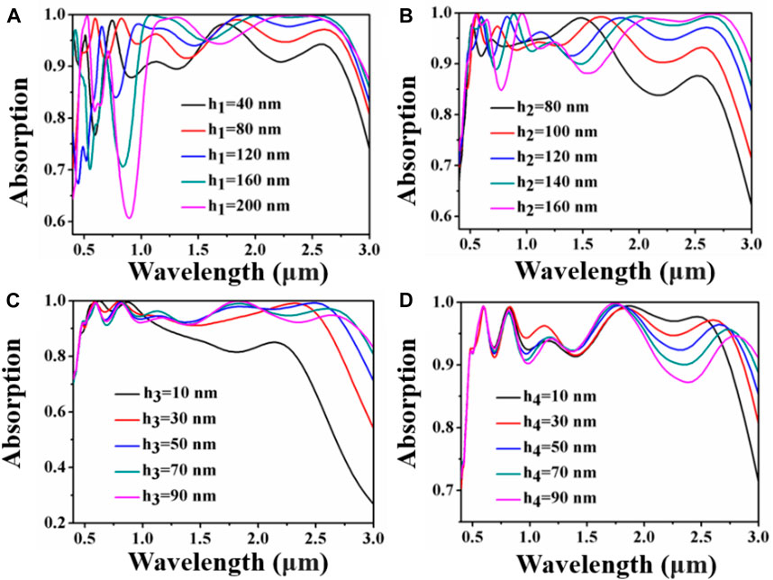
FIGURE 3. (A–D) Absorption spectra corresponding to different geometric parameters.
Next, in order to more clearly and deeply explore the specific physical mechanism behind the broadband absorption phenomenon, we made a detailed analysis of its electromagnetic field distribution, and the results are shown in the Figure 4. The distribution of electric field and magnetic field at the wavelength of 500 nm, 1,500 nm and 2,500 nm of the incident light are plotted with the interval of 1,000 nm. The selected plane is xoz plane, and the top layer of ITO antireflection layer and GaAs grating layer are indicated with black dotted line. When the incident light wavelength is 500 nm, it can be seen from figures (a) and (d) that the electric field is mainly concentrated on both sides of the top structure and the interface with the air, and the magnetic field is distributed in the top two-layer structure, which indicates that in this case, the cavity film and GMRs mode are excited, and the joint effect of the two greatly enhances the overall absorptivity of the structure (Xu et al., 2020). Furthermore, it can be seen from figures (c) and (f) that the light penetrates further to the bottom layer and stronger SPPs are excited. From the corresponding electromagnetic fields of these three bands, we can draw the following conclusion: it is the coupling effect of GMRs, cavity film and SPPs that makes the broadband absorption possible.

FIGURE 4. (A-F) Electromagnetic field distribution of structures at incident wavelengths of 500 nm, 1,500 nm and 2,500 nm (xoz plane).
After the mechanism of broadband absorption of the proposed absorber has been proved, we have further analyzed its other photoelectric characteristics. Similar to the three-layer absorber mentioned above, we simulate the absorption spectrum when the incident angle is 0°–60° and the polarization angle changes from 0° to 90° as shown in the Figure 5. It can be seen from the figure that the designed absorbers have high absorptivity in the range of 0–60° and can withstand large incident angle changes, so the effect is very ideal; For the polarization angle, because the structure is not highly geometrically symmetric, the absorptivity inevitably decreases in the wavelength range of 1,000 nm–1500 nm, but it still maintains a high absorption in the whole wavelength range, and the effect is acceptable. In general, the absorption effect of the proposed absorber is much better than that of the previous absorber, which has better oblique incidence and polarization insensitive characteristics (Cheng et al., 2015; Callewaert et al., 2016; Vafapour, 2019).
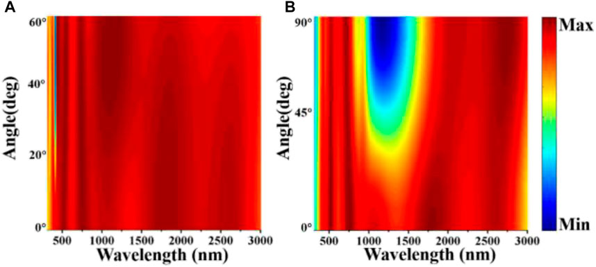
FIGURE 5. (A) Absorption spectra at different oblique incidence angle. (B) Absorption spectra at different polarization angles.
Subsequently, as a solar absorber, the absorption capacity of the actual solar radiation is a very important index (Elshorbagy et al., 2017; Li et al., 2018; Nie et al., 2021; Xie et al., 2021). In order to explore its solar absorption in real situation, we selected AM1.5 spectrum to test its performance, and the results are shown in the Figure 6. In Figure 6A, the black line represents the solar spectrum at AM 1.5, and the red line represents the absorption of the proposed absorber under this solar radiation. It can be clearly seen that the red line and the black line coincide approximately in the whole 400–3000 nm band, which indicates that the efficiency of the absorber is very high and the absorption effect is very ideal. Figure 6B illustrates the previous conclusion more intuitively from the angle of how much energy is absorbed and lost. In the figure, the gray part represents the absorbed energy, and the red part represents the lost part. We can see that there is only a little energy loss in the short band, and it is insignificant compared with the area of the absorbed part. From these two aspects, it is easy to see that the proposed absorber has good practical effect.
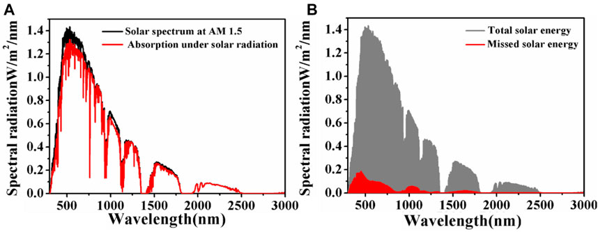
FIGURE 6. (A) Solar energy absorption spectrum (B) Comparison of energy absorption and loss.
We also explore the ideal short-circuit current of the multilayer structure, and the results are shown in Figure 7. It can be seen that the short circuit current of the structure is high. When h2 = 200 nm, the short-circuit current is up to 684.851 A/m2. It can be predicted that the absorber will have a high photoelectric conversion efficiency, making the solar cell have more excellent performance (Mason et al., 2011; El-Gohary et al., 2014; Chen et al., 2019b).
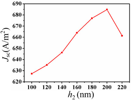
FIGURE 7. Influence of different grating layer thickness on short circuit current.
Conclusion
In this paper, we propose a solar absorber composed of three-layer W-Ti-GaAs films and multi-layer metal semiconductor composite structure of GaAs grating. By adjusting the geometric parameters for many times, the broadband absorption at 500–2,850 nm, up to 2,350 nm, is realized, which greatly broadens the absorption bandwidth of the original simple structure. At the same time, the electromagnetic field distribution of the structure is given, which explains the reason of broadband absorption in physical essence. The spectrum, solar absorption and loss spectrum, ideal short circuit current and other parameters of oblique incidence and polarization angle change are studied, respectively. The results show that our solar absorber can meet the requirements of practical application. The proposed absorber provides theoretical basis for the design of perfect broadband solar absorber.
Data Availability Statement
The original contributions presented in the study are included in the article/Supplementary Material, further inquiries can be directed to the corresponding author.
Author Contributions
MH: Conceptualization, Formal analysis, Investigation, Data curation, Writing - original draft, Writing - review & editing. KW: Conceptualization, Formal analysis, Investigation, Data curation, Funding acquisition. PW: Conceptualization, Formal analysis, Investigation, Data curation, Writing - original draft, Writing - review & editing. DX: Conceptualization, Formal analysis, Revision. YX: Conceptualization, Formal analysis, Revision.
Funding
This work was supported by the National Natural Science Foundation of China (NSFC) (11704223 and 61705056), Zhejiang Provincial Natural Science Foundation of China (LGF20F050004), Research Project of Zhejiang Provincial Department of Education (Y202146019), Research Project of Fujian Provincial Department of Education (JAT190534), Science and Technology Project of Zhejiang University of Technology (KYY-HX-20210657).
Conflict of Interest
The authors declare that the research was conducted in the absence of any commercial or financial relationships that could be construed as a potential conflict of interest.
Publisher’s Note
All claims expressed in this article are solely those of the authors and do not necessarily represent those of their affiliated organizations, or those of the publisher, the editors and the reviewers. Any product that may be evaluated in this article, or claim that may be made by its manufacturer, is not guaranteed or endorsed by the publisher.
References
Cai, R., Rao, W., Zhang, Z., Long, F., and Yin, Y. (2014). An Imprinted Electrochemical Sensor for Bisphenol A Determination Based on Electrodeposition of a Graphene and Ag Nanoparticle Modified Carbon Electrode. Anal. Methods 6, 1590–1597. doi:10.1039/c3ay42125b
Cai, Y., Huang, D., Ma, Z., Wang, H., Huang, Y., Wu, X., et al. (2019). Construction of Highly Conductive Network for Improving Electrochemical Performance of Lithium Iron Phosphate. Electrochimica Acta 305, 563–570. doi:10.1016/j.electacta.2019.02.114
Callewaert, F., Chen, S., Butun, S., and Aydin, K. (2016). Narrow Band Absorber Based on a Dielectric Nanodisk Array on Silver Film. J. Opt. 18 (7), 075006. doi:10.1088/2040-8978/18/7/075006
Cao, G., Li, H., Deng, Y., Zhan, S., He, Z., and Li, B. (2014). Systematic Theoretical Analysis of Selective-Mode Plasmonic Filter Based on Aperture-Side-Coupled Slot Cavity. Plasmonics 9, 1163–1169. doi:10.1007/s11468-014-9727-y
Chen, H.-J., Zhang, Z.-H., Cai, R., Kong, X.-Q., Chen, X., Liu, Y.-N., et al. (2013). Molecularly Imprinted Electrochemical Sensor Based on a Reduced Graphene Modified Carbon Electrode for Tetrabromobisphenol A Detection. Analyst 138, 2769–2776. doi:10.1039/c3an00146f
Chen, P., Liu, F., Ding, H., Chen, S., Chen, L., Li, Y.-J., et al. (2019). Porous Double-Shell CdS@C3N4 Octahedron Derived by In Situ Supramolecular Self-Assembly for Enhanced Photocatalytic Activity. Appl. Catal. B: Environ. 252, 33–40. doi:10.1016/j.apcatb.2019.04.006
Chen, X., Zhou, Y., Han, H., Wang, X., Zhou, L., Yi, Z., et al. (2021). Optical and Magnetic Properties of Small-Size Core-Shell Fe3O4@C Nanoparticles. Mater. Today Chem. 22, 100556. doi:10.1016/j.mtchem.2021.100556
Chen, Z., Chen, H., Jile, H., Xu, D., Yi, Z., Lei, Y., et al. (2021). Multi-band Multi-Tunable Perfect Plasmon Absorber Based on L-Shaped and Double-Elliptical Graphene Stacks. Diamond Relat. Mater. 115, 108374. doi:10.1016/j.diamond.2021.108374
Chen, Z., Chen, H., Yin, J., Zhang, R., Jile, H., Xu, D., et al. (2021). Multi-band, Tunable, High Figure of merit, High Sensitivity Single-Layer Patterned Graphene-Perfect Absorber Based on Surface Plasmon Resonance. Diamond Relat. Mater. 116, 108393. doi:10.1016/j.diamond.2021.108393
Chen, Z., Li, P., Zhang, S., Chen, Y., Liu, P., and Duan, H. (2019). Enhanced Extraordinary Optical Transmission and Refractive-index Sensing Sensitivity in Tapered Plasmonic Nanohole Arrays. Nanotechnology 30, 335201. doi:10.1088/1361-6528/ab1b89
Chen, Z., Zhang, S., Chen, Y., Liu, Y., Li, P., Wang, Z., et al. (2020). Double Fano Resonances in Hybrid Disk/rod Artificial Plasmonic Molecules Based on Dipole-Quadrupole Coupling. Nanoscale 12 (17), 9776–9785. doi:10.1039/d0nr00461h
Cheng, Z., Liao, J., He, B., Zhang, F., Zhang, F., Huang, X., et al. (2015). One-Step Fabrication of Graphene Oxide Enhanced Magnetic Composite Gel for Highly Efficient Dye Adsorption and Catalysis. ACS Sustainable Chem. Eng. 3, 1677–1685. doi:10.1021/acssuschemeng.5b00383
Deng, Y., Cao, G., Wu, Y., Zhou, X., and Liao, W. (2015). Theoretical Description of Dynamic Transmission Characteristics in MDM Waveguide Aperture-Side-Coupled with Ring Cavity. Plasmonics 10, 1537–1543. doi:10.1007/s11468-015-9971-9
Deng, Y., Cao, G., Yang, H., Zhou, X., and Wu, Y. (2018). Dynamic Control of Double Plasmon-Induced Transparencies in Aperture-Coupled Waveguide-Cavity System. Plasmonics 13, 345–352. doi:10.1007/s11468-017-0519-z
El-Gohary, S. H., Choi, J. M., Kim, N.-H., and Byun, K. M. (2014). Plasmonic Metal-Dielectric-Metal Stack Structure with Subwavelength Metallic Gratings for Improving Sensor Sensitivity and Signal Quality. Appl. Opt. 53, 2152–2157. doi:10.1364/AO.53.002152
Elshorbagy, M. H., Cuadrado, A., and Alda, J. (2017). High-sensitivity Integrated Devices Based on Surface Plasmon Resonance for Sensing Applications. Photon. Res. 5, 654–661. doi:10.1364/PRJ.5.000654
Huang, X., He, W., Yang, F., Ran, J., Gao, B., and Zhang, W.-L. (2018). Polarization-independent and Angle-Insensitive Broadband Absorber with a Target-Patterned Graphene Layer in the Terahertz Regime. Opt. Express 26 (20), 25558–25566. doi:10.1364/OE.26.025558
Jiang, L., Yi, Y., Tang, Y., Li, Z., Yi, Z., Liu, L., et al. (2021). A High Quality Factor Ultra-narrow Band Perfect Metamaterial Absorber for Monolayer Molybdenum Disulfide. Chin. Phys. B 19, 103415. doi:10.1088/1674-1056/ac1e11
Jiang, L., Yuan, C., Li, Z., Su, J., Yi, Z., Yao, W., et al. (2021). Multi-band and High-Sensitivity Perfect Absorber Based on Monolayer Graphene Metamaterial. Diamond Relat. Mater. 111, 108227. doi:10.1016/j.diamond.2020.108227
Keshavarz, A., and Vafapour, Z. (2019). Thermo-optical Applications of a Novel Terahertz Semiconductor Metamaterial Design. J. Opt. Soc. Am. B 36, 35–41. doi:10.1364/JOSAB.36.000035
Lei, L., Li, S., Huang, H., Tao, K., and Xu, P. (2018). Ultra-broadband Absorber from Visible to Near-Infrared Using Plasmonic Metamaterial. Opt. Express 26 (5), 5686. doi:10.1364/OE.26.005686
Li, J., Chen, X., Yi, Z., Yang, H., Tang, Y., Yi, Y., et al. (2020). Broadband Solar Energy Absorber Based on Monolayer Molybdenum Disulfide Using Tungsten Elliptical Arrays. Mater. Today Energ. 16, 100390. doi:10.1016/j.mtener.2020.100390
Li, J., Jiang, J., Xu, Z., Liu, M., Tang, S., Yang, C., et al. (2018). Facile Synthesis of Ag@Cu2O Heterogeneous Nanocrystals Decorated N-Doped Reduced Graphene Oxide with Enhanced Electrocatalytic Activity for Ultrasensitive Detection of H2O2. Sensors Actuators B: Chem. 260, 529–540. doi:10.1016/j.snb.2018.01.068
Li, J., Jiang, J., Zhao, D., Xu, Z., Liu, M., Liu, X., et al. (2020). Novel Hierarchical Sea Urchin-like Prussian Blue@palladium Core-Shell Heterostructures Supported on Nitrogen-Doped Reduced Graphene Oxide: Facile Synthesis and Excellent Guanine Sensing Performance. Electrochimica Acta 330, 135196. doi:10.1016/j.electacta.2019.135196
Li, Y., Li, M., Xu, P., Tang, S., and Liu, C. (2016). Efficient Photocatalytic Degradation of Acid orange 7 over N-Doped Ordered Mesoporous Titania on Carbon Fibers under Visible-Light Irradiation Based on Three Synergistic Effects. Appl. Catal. A: Gen. 524, 163–172. doi:10.1016/j.apcata.2015.01.050
Li, Z., Yi, Y., Xu, D., Yang, H., Yi, Z., Chen, X., et al. (2021). A Multi-Band and Polarization-independent Perfect Absorber Based on Dirac Semimetals Circles and Semi-ellipses Array*. Chin. Phys. B 30, 098102. doi:10.1088/1674-1056/abfb57
Li, Z., Yi, Z., Liu, T., Liu, L., Chen, X., Zheng, F., et al. (2021). Three-band Perfect Absorber with High Refractive index Sensing Based on an Active Tunable Dirac Semimetal. Phys. Chem. Chem. Phys. 23 (32), 17374–17381. doi:10.1039/D1CP01375K
Li-Ying, J., Yi, Y. T., Ying-Ting, Y., Zao, Y., Hua, Y., Zhi-You, L., et al. (2021). A Four-Band Perfect Absorber Based on High Quality Factor and High Quality Factor of Monolayer Molybdenum Disulfide. Acta Physica Sinica 70, 128101. doi:10.7498/aps.70.20202163
Liu, Y., Bo, M., Yang, X., Zhang, P., Sun, C. Q., and Huang, Y. (2017). Size Modulation Electronic and Optical Properties of Phosphorene Nanoribbons: DFT-BOLS Approximation. Phys. Chem. Chem. Phys. 19, 5304–5309. doi:10.1039/c6cp08011a
Long, F., Zhang, Z. H., Wang, J., Yan, L., Lu, P. P., and Yang, Z. X. (2016). Magnetic Graphene Modified Imprinted Electrochemical Sensor for Detection of 4-Octylphenol. Chin. J. Anal. Chem. 44, 908–914. doi:10.11895/j.issn.0253.3820.160016
Long, F., Zhang, Z., Wang, J., Yan, L., and Zhou, B. (2015). Cobalt-nickel Bimetallic Nanoparticles Decorated Graphene Sensitized Imprinted Electrochemical Sensor for Determination of Octylphenol. Electrochimica Acta 168, 337–345. doi:10.1016/j.electacta.2015.04.054
Lv, P., Xie, D., and Zhang, Z. (2018). Magnetic Carbon Dots Based Molecularly Imprinted Polymers for Fluorescent Detection of Bovine Hemoglobin. Talanta 188, 145–151. doi:10.1016/j.talanta.2018.05.068
Mason, J. A., Smith, S., and Wasserman, D. (2011). Strong Absorption and Selective thermal Emission from a Midinfrared Metamaterial. Appl. Phys. Lett. 98, 241105. doi:10.1063/1.3600779
Nie, Y., Xie, Y., Zheng, Y., Luo, Y., Zhang, J., Yi, Z., et al. (2021). Preparation of ZnO/Bi2O3 Composites as Heterogeneous Thin Film Materials with High Photoelectric Performance on FTO Base. Coatings 11, 1140. doi:10.3390/coatings11091140
Roostaei, N., Mbarak, H., Monfared, S. A., and Hamidi, S. M. (2021). Plasmonic Wideband and Tunable Absorber Based on Semi Etalon Nano Structure in the Visible Region. Phys. Scr. 96 (3), 035805. doi:10.1088/1402-4896/abdbf6
Sivák, P., Tauš, P., Rybár, R., Beer, M., Šimková, Z., Baník, F., et al. (2020). Analysis of the Combined Ice Storage (PCM) Heating System Installation with Special Kind of Solar Absorber in an Older House. Energies 13 (15), 3878. doi:10.3390/en13153878
Su, J., Yang, H., Xu, Y., Tang, Y., Yi, Z., Zheng, F., et al. (2021). Based on Ultrathin PEDOT:PSS/c-Ge Solar Cells Design and Their Photoelectric Performance. Coatings 11 (7), 748. doi:10.3390/coatings11070748
Tang, N., Li, Y., Chen, F., and Han, Z. (2018). In Situ fabrication of a Direct Z-Scheme Photocatalyst by Immobilizing CdS Quantum Dots in the Channels of Graphene-Hybridized and Supported Mesoporous Titanium Nanocrystals for High Photocatalytic Performance under Visible Light. RSC Adv. 8, 42233–42245. doi:10.1039/c8ra08008a
Vafapour, Z. (2019). Polarization-independent Perfect Optical Metamaterial Absorber as a Glucose Sensor in Food Industry Applications. IEEE Trans.on Nanobioscience 18, 622–627. doi:10.1109/TNB.2019.2929802
Wang, Y., Yi, Y., Xu, D., Yi, Z., Li, Z., Chen, X., et al. (2021). Terahertz Tunable Three Band Narrowband Perfect Absorber Based on Dirac Semimetal. Physica E: Low-dimensional Syst. Nanostructures 131, 114750. doi:10.1016/j.physe.2021.114750
Wu, P., Zhang, C., Tang, Y., Liu, B., and Lv, L. (2020). A Perfect Absorber Based on Similar Fabry-Perot Four-Band in the Visible Range. Nanomaterials 10 (3), 488. doi:10.3390/nano10030488
Xiao, L., Youji, L., Feitai, C., Peng, X., and Ming, L. (2017). Facile Synthesis of Mesoporous Titanium Dioxide Doped by Ag-Coated Graphene with Enhanced Visible-Light Photocatalytic Performance for Methylene Blue Degradation. RSC Adv. 7, 25314–25324. doi:10.1039/c7ra02198d
Xiao, L., Zhang, Q., Chen, P., Chen, L., Ding, F., Tang, J., et al. (2019). Copper-mediated Metal-Organic Framework as Efficient Photocatalyst for the Partial Oxidation of Aromatic Alcohols under Visible-Light Irradiation: Synergism of Plasmonic Effect and Schottky junction. Appl. Catal. B: Environ. 248, 380–387. doi:10.1016/j.apcatb.2019.02.012
Xie, X., Liang, S., Gao, J., Guo, S., Guo, J., Wang, C., et al. (2020). Manipulating the Ion-Transfer Kinetics and Interface Stability for High-Performance Zinc Metal Anodes. Energy Environ. Sci. 13 (2), 503–510. doi:10.1039/c9ee03545a
Xie, Y., Nie, Y., Zheng, Y., Luo, Y., Zhang, J., Yi, Z., et al. (2021). The Influence of β-Ga2O3 Film Thickness on the Optoelectronic Properties of β-Ga2O3@ZnO Nanocomposite Heterogeneous Materials. Mater. Today Commun. 29, 102873. doi:10.1016/j.mtcomm.2021.102873
Xu, F., Lin, L., Wei, D., Xu, J., and Fang, J. (2021). An Asymmetric Silicon Grating Dual-Narrow-Band Perfect Absorber Based on Dielectric-Metal-Dielectric Structure. Front. Mater. 8, 752745. doi:10.3389/fmats.2021.752745
Xu, H., Chen, Z., He, Z., Nie, G., and Li, D. (2020). Terahertz Tunable Optical Dual-Functional Slow Light Reflector Based on Gold-Graphene Metamaterials. New J. Phys. 22 (12), 123009. doi:10.1088/1367-2630/abcc1c
Yi, Z., Li, J., Lin, J., Qin, F., Chen, X., Yao, W., et al. (2020). Broadband Polarization-Insensitive and Wide-Angle Solar Energy Absorber Based on Tungsten Ring-Disc Array. Nanoscale 12, 23077–23083. doi:10.1039/d0nr04502k
Yu, P., Yang, H., Chen, X., Yi, Z., Yao, W., Chen, J., et al. (2020). Ultra-wideband Solar Absorber Based on Refractory Titanium Metal. Renew. Energ. 158, 227–235. doi:10.1016/j.renene.2020.05.142
Zhang, Y., Yi, Z., Wang, X., Chu, P., Yao, W., Zhou, Z., et al. (2021). Dual Band Visible Metamaterial Absorbers Based on Four Identical Ring Patches. Physica E: Low-dimensional Syst. Nanostructures 127, 114526. doi:10.1016/j.physe.2020.114526
Zhang, Z., Cai, R., Long, F., and Wang, J. (2015). Development and Application of Tetrabromobisphenol A Imprinted Electrochemical Sensor Based on Graphene/carbon Nanotubes Three-Dimensional Nanocomposites Modified Carbon Electrode. Talanta 134, 435–442. doi:10.1016/j.talanta.2014.11.040
Zhao, F., Yi, Y., Lin, J., Yi, Z., Qin, F., Zheng, Y., et al. (2021). The Better Photoelectric Performance of Thin-Film TiO2/c-Si Heterojunction Solar Cells Based on Surface Plasmon Resonance. Results Phys. 28, 104628. doi:10.1016/j.rinp.2021.104628
Keywords: solar absorber, finite difference time domain method, broadband absorption, GaAs gratings, photoelectric characteristics
Citation: Huang M, Wei K, Wu P, Xu D and Xu Y (2021) Design of Grating Type GaAs Solar Absorber and Investigation of Its Photoelectric Characteristics. Front. Mater. 8:781803. doi: 10.3389/fmats.2021.781803
Received: 23 September 2021; Accepted: 11 October 2021;
Published: 25 October 2021.
Edited by:
Shifa Wang, Chongqing Three Gorges University, ChinaReviewed by:
Yougen Yi, Central South University, ChinaChao Liu, Northeast Petroleum University, China
Chen Zhiquan, Hunan University, China
Copyright © 2021 Huang, Wei, Wu, Xu and Xu. This is an open-access article distributed under the terms of the Creative Commons Attribution License (CC BY). The use, distribution or reproduction in other forums is permitted, provided the original author(s) and the copyright owner(s) are credited and that the original publication in this journal is cited, in accordance with accepted academic practice. No use, distribution or reproduction is permitted which does not comply with these terms.
*Correspondence: Yan Xu, eHV5YW5oenVAMTI2LmNvbQ==