 Chandan Kumar
 Sanjeev Kumar Raghuwanshi
 Vikram Kumar
- 1Department of Electronics Engineering, Indian Institute of Technology (Indian School of Mines) Dhanbad, Dhanbad, Jharkhand, India
- 2Department of Electronics & Communication Engineering, I.T.S Engineering College, Greater Noida, UP, India
- 3Department of Electronics Science, Delhi University, New Delhi, India
One of the strongest and thinnest substances known to exist is graphene. It can be efficiently used for antenna fabrication and significant benefits can be analyzed such as size miniaturization, gain and return loss enhancement, flexibility and increase in bandwidth, etc. In this paper, a graphene patch antenna has been designed and fabricated for 5G applications at 28.3 GHz. Different 5G frequency allocation throughout the world is shown in tabular form. Photonic crystal substrate is used to reduce surface wave loss which in turn, increases the radiation efficiency of the antenna. The ground plane is made up of copper, treated as a Perfect Electric Conductor Several unique properties of graphene are analyzed and shown. Then, a thin graphene sheet is used as a patch and an antenna is designed and fabricated. The patch has dimensions of 3.4 mm by 2.38 mm. The simulated return loss is maximum at −33.69 dB at 28.3 GHz, whereas for the measured design it is −26.31 dB at 28.04 GHz. It is observed that graphene can be a good alternative to existing conductors, especially at higher frequencies. The proposed antenna is designed and simulated using HFSS software.
Introduction
Massive advancement in the field of communication leads towards the fifth-generation technology commonly known as 5G. It is the wireless communication standard after the fourth generation (4G/IMT). The standard document of 5G had been published by 3GPP and officially approved in the Plenary Meeting in June 2018. It has been developed to provide next-generation user experiences, enable new deployment patterns, and deliver new services. 5G will push the mobile environment into new worlds with its fast speeds, greater reliability, and low latency.
Various countries have different frequency spectrum allocations for mobile communication. Millimeter wave bands (26, 28, 38, and 60 GHz) will be used for 5G communication in general (IMT-2020, 2020; Shimodaira et al., 2015; Marcus, 2016) as shown in Table 1. It is 24.5–29.5 GHz for India, while the FCC has allotted an extraordinary 7 GHz of un-channelized spectrum for license-free operation between 57 and 64 GHz (Kao et al., 2013; Wang et al., 2016). This makes it possible for anyone to create apps that operate in this frequency range in order to fully utilize this spectrum for their needs.
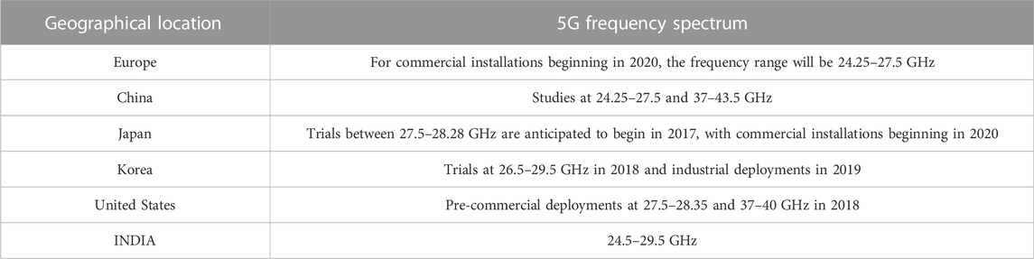
TABLE 1. 5G frequency band spectrum of different geographical areas.
Designing an antenna at such a high frequency band is a real challenge due to its compact size and wide band requirement to incorporate the entire accessible band. The microstrip patch antenna is one of the most useful antennae due to its several advantages such as low weight, compact size, conformal to planer and non-planer surfaces and ease of fabrication and lower fabrication cost etc. It has various shapes e.g., rectangular, square, circle and can be easily etched on any PCB (Balanis, 2005).
The low efficiency, narrow bandwidth, and lower gain of microstrip antennas is a major operational drawback. To boost the bandwidth and gain of the microstrip patch antenna, some strategies such as raising the substrate thickness or patch size were used. However, a thicker substrate reduces radiation efficiency due to greater surface wave losses. Because it can limit surface wave propagation and improve the electrical performance of the micro-strip patch antenna, photonic crystal substrate is a superior answer to this problem. The photonic crystal is a non-natural material made of periodic implant structure within the surrounding medium, which might be dielectric or conductor. Scattering and diffraction properties of periodic structures greatly affect the electromagnetic wave propagation through them. So, antennas with photonic crystals have many unique characteristics (Ozbay et al., 2003; Gonzalo et al., 1999; Meade et al., 1993; Gonzalo et al., 21312138).
Graphene has recently attracted tremendous interest in various research areas due to its exceptional electrical and mechanical properties (Geim and Novoselov, 2007). Graphene is a hexagonally organized honeycomb lattice material with great mobility (8000 cm2/V), 5000 W/m/K thermal conductivity, and observable flexibility (Novoselov et al., 2004; Geim and Novoselov, 2007; Song et al., 2018). In general, the conductivity of graphene is very frequency-dependent and can have completed different behaviour e.g., at microwave and THz. Recently, graphene has gained a lot of attention as a material and has various uses in the microwave to the mm-wave range (Warner et al., 2013; Bozzi et al., 2015). But, the application of graphene in passive guided devices and antennas from microwaves to THz has been by far less exploited.
The use of graphene material as conducting substance for the patch is speculated to enhance the bandwidth and radiation efficiency of the antenna due to its stand-out functionalities and electromagnetic properties. So, several works have been published using graphene as antennas, couplers, filters, amplifiers and other telecommunication devices.
Wang et al. (2015) presented the concept of the graphene-based two-dimensional leaky-wave antenna (LWA), allowing both frequency tuning and beam steering in the terahertz (THz) band. Goyal and Vishwakarma (Goyal and Kumar Vishwakarma, 2018) investigated the effect of graphene’s chemical potential on return loss and resonant frequency of the antenna; Mojtaba and Carey (Dashti and David Carey, 2018) show a graphene antenna with dynamic conductivity to produce a surface impedance microstrip antenna with a bandwidth of hundreds of GHz. In Qu et al. (2018) proposed a frequency-selective surface (FSS) with tunable band stop performance.
The choice of substrate is also very important for obtaining efficient antennas. Photonic band gaps (PBGs) have been increasingly used in order to improve the performance and characteristics of antenna designs (Choudhury et al., 2016).
Conventional metallic patch antennas suffer from high propagation and scattering losses in the environment. So, graphene-based antennas can be used as an alternative. Azizi et al. (2017) compared the different characteristics of a graphene-patch antenna with the conventional copper-patch antenna in the THz frequency band. It shows the return loss increases from −15 to −29 dB and gain improves to 7.16 dB when graphene is used as patch material while it was 5.63 dB when the conventional copper patch was used.
This paper presents a microstrip antenna on a photonic crystal substrate in which graphene may be used as patch material. But due to fabrication limitations, copper is used instead of graphene. The rest of this paper is organized as follows: Section 2 describes graphene and its properties. Antenna design on photonic crystal substrate is discussed in Section 3. Simulated and measured results are discussed in Section 4. Section 5 concludes the paper.
Graphene and its properties
Graphene is used as conducting patch material which is the two-dimensional version of graphite. In graphene, the energy-momentum relationship for electrons is linear over a wide range of energies, rather than quadratic, so electrons in graphene behave as massless relativistic particles “Dirac fermions” with an energy-independent velocity (Wallace, 1947; Geim and Novoselov, 2007; Charlier et al., 2008). It is a zero-overlap semimetal (with both holes and electrons as charge carriers) with very high electrical conductivity as shown in Figure 2. High charge carrier mobility, for which values of 10,000 cm2/Vs., in some cases even 200,000 cm2/Vs were reported. Its surface conductivity is frequency dependent and can be described using Kubo’s formula approximation (Gusynin et al., 2007) in its most simplified form given by
where -e is the electronic charge, ℏ = ℎ/2Π is the reduced Planck’s constant.
fd (ε) = [e kBT+ 1 ]−1 is the Fermi-Dirac distribution and kB is the Boltzmann’s constant
ω is radian frequency, μc is chemical potential, Γ is a phenomenological scattering rate, that is, assumed to be independent of energy ε and T is temperature. The first term in Eq. 1 is due to intraband contributions, and the second term to interband contributions. Surface conductivity dependency on frequency is shown in graphical form, which is achieved using MATLAB simulation. Here, μc is taken as 0ev which represents the worst case (Hanson, 2008).
Figure 1 shows conductivity plot with frequency, keeping the chemical potential as zero for a graphene flake within the GHz-THz band. Because of its two-dimensional crystalline structure and exceedingly thin layer height, graphene is thought of as having a lattice structure. The minimal thickness is considered from the perspective of electromagnetic simulation so that the EM field distribution may observe the thickness of the graphene and wave propagation can happen.
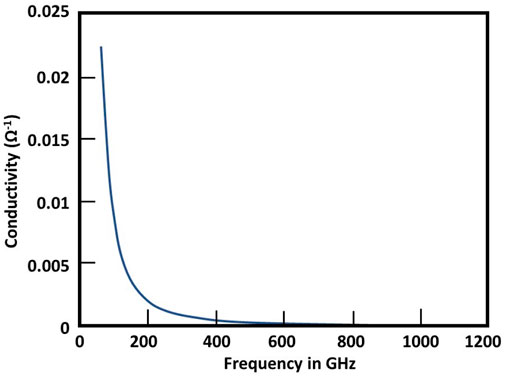
FIGURE 1. Graphene’s Conductivity vs. Frequency graph represented as by Kubo’s formula (Gusynin et al., 2007).
From the figure, it can be seen that the conductivity of graphene shows inductive nature and it allows infinite graphene sheet to support Transverse Magnetic surface waves, which is referred to as Surface Plasmon Polariton (SPP), since the conductivity results from the plasma-like behaviour of electrons [ 25].
An electron attached to an atom in an insulator or semiconductor can only break free if it receives enough energy from heat or a passing photon to cross the “band gap”. However, with graphene, the gap is infinitesimally small, as illustrated in Figure 2A. This is the primary reason why graphene electrons flow so readily and quickly. Figure 2B depicts a freestanding graphene with the valence and conduction energy bands, denoted by Π and Π∗ bands, exhibiting a linear (conical) relationship between electron energy and momentum and intersecting at particular momentum positions K and K′ (left). Conrad and colleagues (Geim and Novoselov, 2007; Nevius et al., 2015) demonstrated that, while the first carbon layer of samples grown epitaxially on a silicon carbide substrate at around 1340°C is electronically inert and thus lacks a band structure (middle), at growth temperatures 20°C higher, the layer becomes active and demonstrates and Π and Π∗ bands separated by a gap of 0.5 electron volts around the K and K′. Because of this peculiar dispersion relationship, graphene is a zero-gap substance that conducts electrons like a metal.
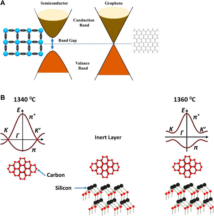
FIGURE 2. Energy band diagram of Graphene. (A) Shows zero bandgap between Conduction and Valance band. (B) Shows the temperature dependency of the energy band of graphene.
The particles in each valley can formally be described by Dirac-like Hamiltonian (Geim and Novoselov, 2007)
where K is the quasiparticle momentum, σ is the 2D Pauli matrix and k-independent Fermi velocity vF plays the role of the speed of light.
Graphene fabrication
A unique process for fabricating patch antenna with graphene is presented by (Sajal and Braaten, 2015) at the resonant frequency of 2.6 GHz. In this paper, a thin graphene sheet is pated on 100 µm thick paper and cut in the shape of a patch using g commercially available micro-cutter. Another fabrication approach is given by Zhou et al. (2020) in which a conductive ink was made by mixing graphene flakes with N-Methyl-pyrrolidone (NMP) then, the desired pattern was printed on a paper substrate using screen-printing technology. The operating frequency is 5.8 GHz for wireless communication applications. A graphene-based bow-tie antenna is designed by (Avsar Aydin, 2021) for biomedical applications using 3-D printing technology. Conductive Graphene PLA filament for the core of the antenna and standard PLA for the dielectric substrate parts is used in this design. It provides an ultra-wide bandwidth of 18 GHz in the frequency range of 2–20 GHz for ultra-wideband applications.
4 Antenna design and fabrication
A microstrip antenna is made up of a metallic patch on top of a dielectric substrate with a metallic conductor beneath it to serve as a ground plane. Different characteristics of antenna such as resonant frequency, bandwidth, gain, return loss, radiation pattern etc. depends on the substrate, patch dimension and feed type. This proposed antenna is designed on a photonic crystal using FR4 material (ɛr = 4.4 and loss tangent tan δ = 0.002) which acts as a substrate as shown in Figure 3.
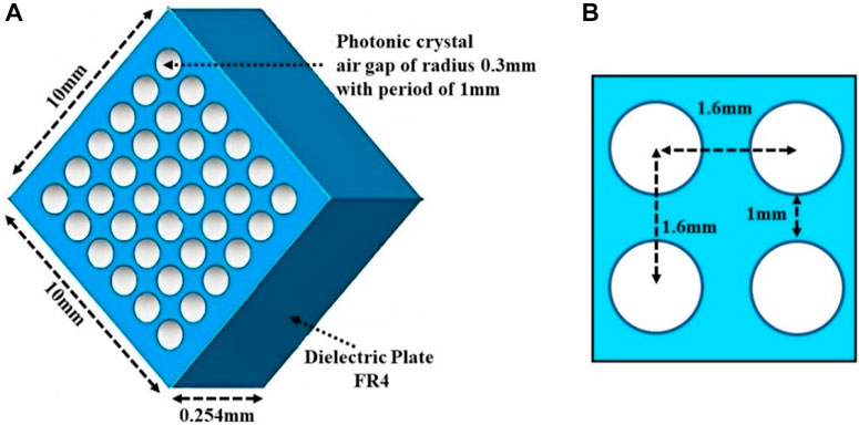
FIGURE 3. (A) Schematic of Photonic crystal with cylindrical air gap used for antenna designing (B) Primitive cell structure showing periodic gap between air cylinders.
Figure 3 shows the proposed photonic crystal with an air gap in the dielectric slab. FR4 (relative permittivity of 4.4 and dielectric loss tangent of 0.002) is used as a substrate. An air gap hole of radius 0.3 mm with a period of 1 mm is taken and embedded in the pattern of six rows along length and six columns along the width, i.e., a total number of 36 cylindrical air holes are created as shown in figure. A much closer view of the photonic band gap crystal is shown in Figure 3B where cylindrical radius and periods are mentioned. The proposed substrate has length, width, and height of 10 mm, 10 mm and 0.254 mm respectively. As shown in Figure 4 & Figure 5.
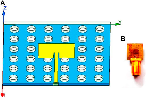
FIGURE 4. (A) Simulated antenna structure (B) fabricated patch antenna.
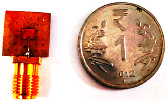
FIGURE 5. Size approximation of fabricated Patch Antenna and compare with rupee coin.
The performance of the microstrip antenna is dependent on its size, operating frequency, radiation efficiency, directivity, and other criteria (Balanis, 2005). For effective radiation, the following equations are utilized in calculations:
The practical width of the patch is calculated using equation (Gonzalo et al., 21312138)
Where v0 is the free space velocity of light.
The effective dielectric constant,
Where ɛr is the dielectric constant of the material, w is the width of the patch, and h is the height of the substrate.
Prolonged electrical length, ΔL of the patch due to the fringing effect can be calculated using (Balanis, 2005)
The effective length, Leff is given (Balanis, 2005)
The proposed antenna has a rectangular radiating patch excited with strip line feeding for 50 Ω characteristic impedance. Conducting patch has a dimension of 3.4 mm × 2.38 mm and a thin copper sheet of thickness 0.01 mm is used for it. FR4 is used as the substrate (dielectric constant
Fabrication steps
Due to fabrication limitations, FR4 with copper coating is used instead of graphene. This antenna was fabricated using photolithographic process. Table 2 shows the dimensions of the proposed antenna. This process constitutes an Ultraviolet light (UV ray) of the corresponding wavelength and desired photo-resist. Negative and positive photo-resist materials are there. The exposed portion of negative photo-resist hardens when the photo-resist developer is applied to it. Whereas in the case of positive photo-resist the exposure to the UV light changes the chemical structure of the resistor so that it becomes more soluble in the developer.
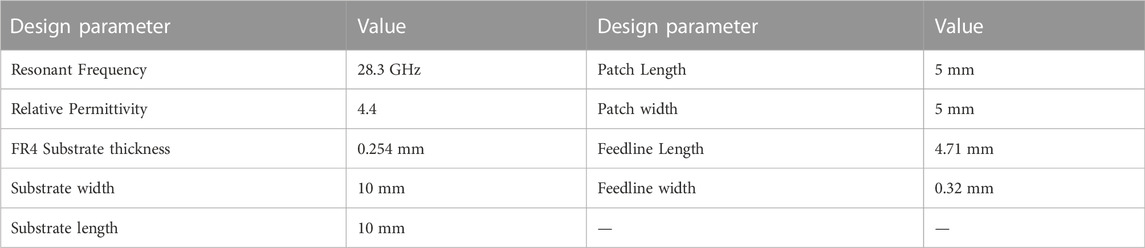
TABLE 2. Optimized dimensions of Patch antenna.
Flow chart of the fabrication steps is shown in Figure 6. In this fabrication, we use positive photo-resist (DNQ-Novolac photo-resist) for fabrication. Firstly, a double-sided copper coated FR4 substrate is taken. DNQ thin film is applied as lamination on overall substrate and copper layer on both side is completely etched out using FeCl3 solution. This substrate in properly rinsed in clean running water to remove any impurities and then dried. In the next step, cylindrical holes of radius 0.3 mm are drilled in a periodic manner with separation of 1 mm. Substrate is properly cleaned again to eliminate any particle on it so that resonant frequency of antenna remains unaltered. With the help of non-dielectric adhesive solution, a very thin copper sheet is pasted on lower side of the substrate which acts as ground plane and patch of calculated size is pasted over it. Temperature is maintained at 200°C for proper pasting of sheets. Since non-dielectric adhesive solution is used, relative permittivity remains unaltered. Step by step fabrication process is illustrated in Figure 7.

FIGURE 6. Flow chart of fabrication process.
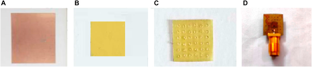
FIGURE 7. (A) FR4 substrate with a copper coating (B) etched FR4 (C) cylindrical holes of 0.3 mm is drilled in the substrate (D) Copper patch is pasted on Substrate.
Results and discussion
First of all, the proposed antenna is designed on a normal FR4 substrate and return loss is analyzed. Then, photonic bandgap substrate is formed by implanting the cylindrical holes within the substrate periodically. The hole radius varies from 0.1 mm to 0.3 mm with a step size of 0.1 mm and its effect is shown in Figure 8. It can be seen that results are improved in terms of return loss, gain and bandwidth. A tabular comparison is shown in Table 3. As the hole radius changes, different characteristics of the antenna also change which is analyzed here and the 0.30 mm radius has the lowest return loss −33.69 dB. This lowest return loss occurs at 28.3 GHz having a bandwidth 1.30 GHz and gain of 3.13 dB, also these two parameters are higher in comparison to other parametric optimization results.
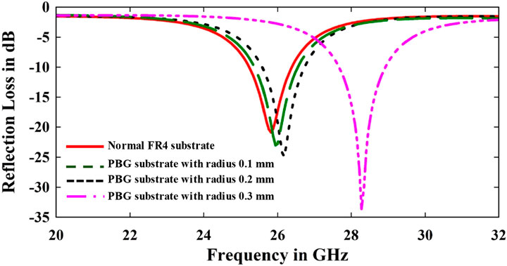
FIGURE 8. Simulated return loss with varying cylindrical radius.

TABLE 3. Summarizes the effect of change in radius of cylindrical holes.
As the radius of the cylindrical air gap changes, air FR4 substrate volume also changes. With the increase in the air gap radius, the total available FR4 substrate volume decreases which, in terms, affects the relative permittivity of the substrate and this can be determined by observing Table 4. As mentioned air gap radius of 0.3 mm has a total available FR4 substrate volume of 22.808 mm3.
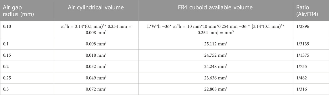
TABLE 4. Cylindrical air gap volume Vs. FR4 Volume correlation of proposed antenna.
Figure 9 shows simulated versus measured return loss of proposed antenna. Solid lines show the simulated result whereas the dashed line represents the measured one. Simulated return loss is found to be −33.69 dB at 28.3 GHz whereas measured in S11 is −26.31 dB at 28.04 GHz as shown in Figure 9. The simulated bandwidth is found as 1.3 GHz whereas the measured bandwidth is 0.89 GHz which is in close proximity to the simulated one.
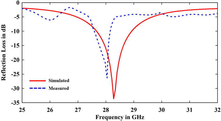
FIGURE 9. Simulated vs. Measured return loss.
The far field radiation patterns (both E-plane and H-plane) of the fabricated antenna were measured in a fully equipped anechoic chamber as shown in Figure 10. Antenna Under Test is placed on an ETS Lindgren 2090 positioner and aligned to the reference horn antenna with adjustable polarization.
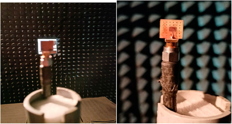
FIGURE 10. Electrical Characterization of fabricated antenna in Anechoic chamber.
Surface current density distribution is shown in Figure 11. The current distribution is zero at the ends of the patch because the current can’t flow “off” the patch. The voltage is out of phase with the current. The current density at the resonant frequency shows a greater amount of accumulated current on the radiating patch. Simulated VSWR is shown in Figure 12A and is 1.047 at the resonant frequency of 28.29 GHz which is a well-accepted value. Also, Figure 12B, shows the Gain result where the maximum Gain can be seen as 3.6 dB at zero degrees theta. By varying the photonic crystal hole radius on the substrate, the lowest return loss -33.69 dB has been obtained among other optimization. The resonant frequency for the lowest return loss value is 28.3 GHz having a bandwidth 1.30 GHz and gain of 3.13 dB and is higher among other results. The result shows the radius of holes 0.03 mm is useful in designing. Further, this fabricated antenna can be used for recent 5G applications since resonant frequency lies within India’s 5G frequency spectrum. In the future, such photonic crystals required to test and analyze in different natural environments and temporal conditions.
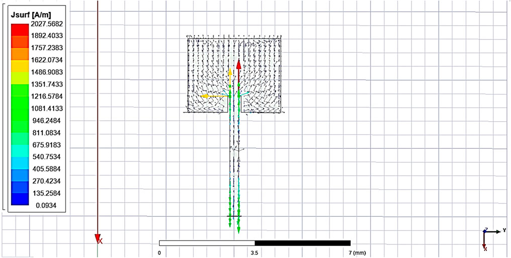
FIGURE 11. The surface current density distribution of the antenna at the resonance frequency.
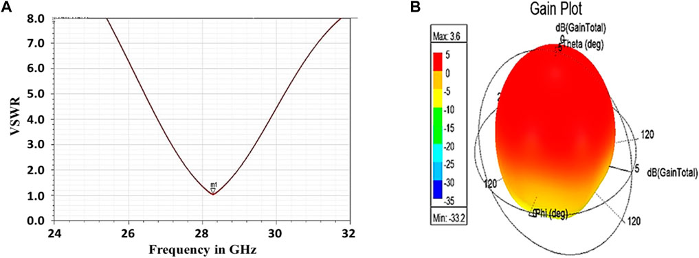
FIGURE 12. (A) Simulated VSWR of a rectangular microstrip patch antenna on photonic crystal and (B) 3-D plot of far-field gain at the resonant frequency of 28.3 GHz.
Conclusion
This research article shows the design and development of a rectangular microstrip patch antenna on the photonic crystal designed and simulated using HFSS with a resonant frequency of 28.3 GHz. Then, this antenna is fabricated using a photolithography process which is explained in brief. Electrical characterization of the antenna is done in the semi-anechoic chamber and measured results are in close proximity to the simulated one. Parametric optimization of the radius of cylindrical holes summarizes as the hole radius changes, different characteristics of the antenna also change which is analyzed here. The lowest return loss −33.69 dB occurs at 28.3 GHz having a bandwidth 1.30 GHz and gain of 3.13dB, and is higher in comparison to other parametric optimization results. With the increase in the air gap radius, the total available FR4 substrate volume decreases which, in terms, affects the relative permittivity of the substrate. Moreover, the surface current density has been observed and the current distribution is zero at the ends of the patch because the current can’t flow “off” the patch. Further, this fabricated antenna can be used for recent 5G applications since resonant frequency lies within India’s 5G frequency spectrum.
Data availability statement
The original contributions presented in the study are included in the article/Supplementary Material, further inquiries can be directed to the corresponding author.
Author contributions
All authors listed have made a substantial, direct, and intellectual contribution to the work and approved it for publication.
Funding
This work is carried out from Research Grant under Grant number: ERIP/ER/202206004/M/01/1805 (Sanction Code of ER&IPR: DGTM/ERIP/GIA/22-23/115/008 dated 08/08/2022) provided by Defense Research and Development Organization (DRDO), Government of India (GOI) under Extramural Research funding scheme with the project entitled “Design and Development of Frequency Stable and High Q-Factor Optoelectronic Oscillator Assisted by Microwave Photonic Techniques”. Project Reference number of Indian Institute of Technology (ISM) Dhanbad-826004 is DRDO (19)/2022-2023/914/ECE.
Conflict of interest
The authors declare that the research was conducted in the absence of any commercial or financial relationships that could be construed as a potential conflict of interest.
Publisher’s note
All claims expressed in this article are solely those of the authors and do not necessarily represent those of their affiliated organizations, or those of the publisher, the editors and the reviewers. Any product that may be evaluated in this article, or claim that may be made by its manufacturer, is not guaranteed or endorsed by the publisher.
References
Avsar Aydin, E. (2021). 3D-Printed graphene-based bow-tie microstrip antenna design and analysis for ultra-wideband applications. Polym. 13 (21), 3724. doi:10.3390/polym13213724
Azizi, Mohamed K., Ksiksi, Mohamed A., Ajlani, Hosni, and Ali, Gharsallah (2017). Terahertz graphene-based reconfigurable patch antenna. Prog. Electromagn. Res. Lett. 71 (69–76), 69–76. doi:10.2528/pierl17081402
Bozzi, M., Pierantoni, L., and Bellucci, S. (2015). Applications of graphene at microwave frequencies. Radioengineering 24, 661–669. doi:10.13164/re.2015.0661
Charlier, J. C., Eklund, P. C., Zhu, J., and Ferrari, A. C. (2008). Electron and phonon properties of graphene: Th eir relationship with carbon nanotubes. Top. Appl. Phys. 111, 673–709.
Choudhury, B., Danana, B., and Jha, R. M. (2016). PBG based terahertz antenna for aerospace applications. SpringerBriefs in electrical and computer engineering. Singapore: Springer.
Dashti, M., and David Carey, J. (2018). Graphene microstrip patch ultrawideband antennas for THZ communications. Adv. Funct. Mat. 28, 1705925. doi:10.1002/adfm.201705925
Geim, A. K., and Novoselov, K. S. (2007). The rise of graphene. Nat. Mater 6, 183–191. doi:10.1038/nmat1849
Gonzalo, R., De Maagt, P., and Sorolla, M. (1999). Enhanced patch-antenna performance by suppressing surface waves using photonic-bandgap substrates. IEEE Trans. Microw. Theory Tech. 47 (11), 2131–2138. doi:10.1109/22.798009
Gonzalo, R., Martinez, B., and de Maagt, P. (1999). The effect of dielectric permittivity on the properties of photonic bandgap devices. Microw. Opt. Technol. Lett 23 (2), 92–95. 92{95. doi:10.1002/(sici)1098-2760(19991020)23:2<92:aid-mop9>3.0.co;2-j
Goyal, R., and Kumar Vishwakarma, D. (2018). Design of a graphene-based patch antenna on glass substrate for highspeed terahertz communications. Microw. Opt. Technol. Lett. 60, 1594–1600. doi:10.1002/mop.31216
Gusynin, V. P., Sharapov, S. G., and Carbotte, J. P. (2007). Magneto-optical conductivity in graphene. J. Phys. Condens. Matter 19, 026222. doi:10.1088/0953-8984/19/2/026222
Hanson, G. W. (2008). Dyadic Green’s functions and guided surface waves for a surface conductivity model of graphene. J. Appl. Phys. 103, 064302. doi:10.1063/1.2891452
Imt-2020, (2020). ITU towards “IMT for 2020 and beyond” - IMT-2020 standards for 5G. Geneva, Switzerland: International Telecommunications Union. Retrieved 02 22, 2017).
Kao, T. J., Yan, Y., Shen, T. M., Chen, A. Y. K., and Lin, J. (2013). Design and analysis of a 60-GHz CMOS Doppler micro-radar system-in-package for vital-sign and vibration detection. IEEE Trans. Microw. Theory Tech. 61 (4), 1649–1659. doi:10.1109/tmtt.2013.2247620
Marcus, M. (2016). WRC-19 issues: Agenda item 1.15 and the use of 275–450 GHz”. Dec. USA: IEEE Wireless Comm, 2–3.
Meade, R. D., Rappe, A. M., Brommer, K. D., and Joannopoulos, J. D. (1993). Nature of the photonic band gap: Some insights from a field analysis. J. Opt. Soc. Am. B 10, 328–332. doi:10.1364/josab.10.000328
Nevius, M. S., Conrad, M., Wang, F., Celis, A., Nair, M. N., Taleb-Ibrahimi, A., et al. (2015). Semiconducting graphene from highly ordered substrate interactions. Phys. Rev. Lett. 115, 136802. doi:10.1103/physrevlett.115.136802
Novoselov, K. S., Geim, A. K., Morozov, S. V., Jiang, D., Zhang, Y., Dubonos, S. V., et al. (2004). Electric field effect in atomically thin carbon films. Science 306, 666–669. doi:10.1126/science.1102896
Ozbay, E., Temelkuran, B., and Bayindir, M. (2003). Microwave applications of photonic crystals. Prog. Electromagn. Res. PIER 41, 185–209. doi:10.2528/pier02010808
Qu, M., Song, J., Yao, L., Li, S., Deng, L., and Yang, Y. (2018). Design of a graphene based tunable frequency selective surface and its application for variable radiation pattern of a dipole at terahertz. Radio Sci. 53 (2), 183–189. doi:10.1002/2017rs006401
Sajal, Sayeed Z., and Braaten, Benjamin D. “A microstrip patch antenna manufactured with flexible graphene-based conducting material,” in Proceedings of the 2015 IEEE International Symposium on Antennas and Propagation & USNC/URSI National Radio Science Meeting, Vancouver, BC, Canada, July 2015. doi:10.1109/APS.2015.7305596
Shimodaira, H., Tran, G. K., Sakaguchi, K., and Araki, K. (2015). “Investigation on millimeter-wave spectrum for 5G,” in IEEE Conference on Standards for Communications and Networking (CSCN), 143–148.
Song, R., Wang, Q., Mao, B., Wang, Z., Tang, D., Zhang, B., et al. (2018). Flexible graphite films with high conductivity for radio-frequency antennas. Carbon 130, 164–169. doi:10.1016/j.carbon.2018.01.019
Wallace, P. R. (1947). Th e band theory of graphite. Phys. Rev. 71, 622–634. doi:10.1103/physrev.71.622
Wang, R., Gao, P., Wang, P., and Kang, K. (2016). A planar end-fire antenna with wide beamwidth for 60 GHz applications. Prog. Electromagn. Res. Lett. 61, 125–130. doi:10.2528/pierl16061902
Wang, X., Zhao, W., Hu, J., and Yin, W. (2015). Reconfigurable terahertz leaky-wave antenna using graphene-based high-impedance surface. IEEE Trans. Nanotechnol. 14, 62–69. doi:10.1109/tnano.2014.2365205
Warner, J. H., Schaffel, F., Rummeli, M., and Bachmatiuk, A. (2013). Graphene fundamentals and emergent applications. Oxford, UK: Elsevier.
Zhou, Xinyao, Ting, Leng, Pan, Kewen, Abdalla, Mahmoud A., and Hu, Zhirun “Graphene printed flexible and conformal array antenna on paper substrate for 5.8GHz wireless communications,” in Proceedings of the 14th European Conference on Antennas and Propagation (EuCAP), Copenhagen, Denmark, March 2020. doi:10.23919/EuCAP48036.2020.9135742
Keywords: microstrip antenna, 5G, graphene, photonic crystal substrate, gain, return loss
Citation: Kumar C, Raghuwanshi SK and Kumar V (2022) Graphene based microstrip patch antenna on photonic crystal substrate for 5G application. Front. Mater. 9:1079588. doi: 10.3389/fmats.2022.1079588
Received: 25 October 2022; Accepted: 07 December 2022;
Published: 23 December 2022.
Edited by:
Chandan Kumar, Nara Institute of Science and Technology (NAIST), JapanReviewed by:
Shatrughna Kumar, Tel Aviv University, IsraelYongqiang Yu, Hefei University of Technology, China
Copyright © 2022 Kumar, Raghuwanshi and Kumar. This is an open-access article distributed under the terms of the Creative Commons Attribution License (CC BY). The use, distribution or reproduction in other forums is permitted, provided the original author(s) and the copyright owner(s) are credited and that the original publication in this journal is cited, in accordance with accepted academic practice. No use, distribution or reproduction is permitted which does not comply with these terms.
*Correspondence: Vikram Kumar, ZHJ2aWtyYW0uZWFydGhAZ21haWwuY29t