 Dong Ji
 Srabanti Chowdhury
- 1School of Science and Engineering, The Chinese University of Hong Kong, Shenzhen, China
- 2Department of Electrical Engineering, Stanford University, Stanford, CA, United States
We present a review of GaN avalanche photodiodes. GaN-based avalanche photodiodes are of emerging interest to the device community. The review covers various important aspects of the device such as the design space, substrate choice, edge termination efficacy, and last, but not least, the physics behind the avalanche breakdown in GaN. The study comprehends the reported impact ionization coefficients and how they may affect the device performances. Finally various reported GaN APDs are summarized and compared. We conclude that hole-initiated GaN APDs on free-standing GaN substrates can offer unprecedented advantages as ultraviolet light detectors, due to their ultra-high responsivity and low dark current.
Introduction
High gain ultraviolet (UV) light detectors are significant for various applications, such as medical imaging, optical communication, flame detection, chemical sensing, sterilization and purification, ozone sensing and detection, and various other emerging imaging applications for security. Currently, the dominant UV light detectors are based on photomultiplier tubes, which suffer from the high cost and low lifetime (Zheng et al., 2020). Solid-state-based avalanche photodiodes (APDs) look attractive for UV light detections since they can change the landscape of UV detection by offering more durability, lower cost, and surpassing the performance of a tube-based multiplier. The APD is a highly sensitive photodetector that converts a light signal to an electrical signal and amplifies it by taking advantage of the carriers’ multiplication during impact ionization and avalanche (Sze and Ng, 2006).
Impact ionization occurs in a semiconductor when one energetic carrier, either an electron or a hole, loses its energy after scattering with the crystal lattice and generates more energetic electrons and holes. The generated electrons and holes continue to travel through the high electric field region where they continue to accelerate and eventually lose their energy to scattering with the crystal lattice, generating more and more carriers. This phenomenon leads to the multiplication of carriers leading to an avalanche breakdown in the device. However, when properly controlled the impact ionization process can be of great use for enabling various high frequency, high power amplifiers, and detectors. Figure 1 schematically illustrates the impact ionization process in a reverse-biased p-i-n junction to highlight the multiplication process.
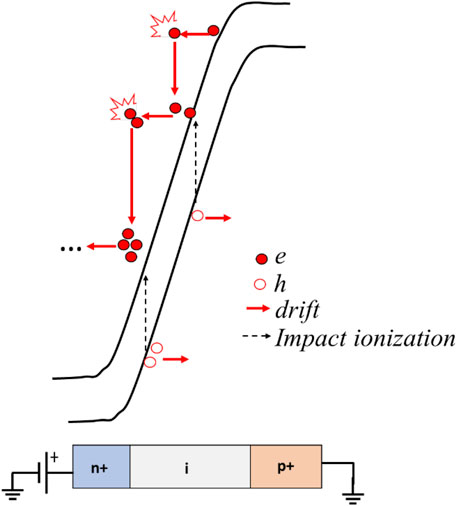
FIGURE 1. Impact ionization process in a reverse-biased p-i-n junction.
The condition of avalanche often needs to be defined quantitatively for practical use of the phenomenon in devices. For instance, the multiplication factor, M, can be mathematically written as the following equation:
where V is the applied voltage and BV is the avalanche breakdown voltage.
In APDs, when the applied voltage is less than the BV, the device works in the linear mode. When the applied voltage equals to the BV, the multiplication factor tends to infinity, and the Geiger mode is triggered in an APD, which can be used appropriately for single-photon detections (Hu, 2008; Hadfield, 2009; Zhang, 2011).
Owing to its bandgap of 3.4 eV and large electric field tolerance, GaN has exceptional advantages as APDs, serving various applications, particularly those that require high temperature and harsh environment tolerance.
To enable a GaN APD with robust avalanche capability, we have noted from our studies (Ji D. et al., 2019; Ji et al., 2020a; Ji et al., 2020b; Ji and Chowdhury, 2020) the following two requirements: 1) presence of high-quality epitaxial layers, which is possible when grown on free-standing GaN substrates; 2) optimized edge terminations to eliminate both localized peak electric field and dark leakage in the device.
Due to the absence of natural GaN substrates, GaN film growths for devices were primarily developed on foreign substrates, such as sapphire, silicon, or silicon carbide (Amano, 2015; Liu and Edgar, 2002; Krost and Dadgar, 2002; Mion et al., 2006). Constrained by the lattice mismatch, as shown in Figure 2, the GaN films are amenable to a large number of defect densities in the order of 109 or 108 cm−2 (Amano, 2015; Liu and Edgar, 2002; Krost and Dadgar, 2002; Mion et al., 2006). Such defects can severely inhibit the impact ionization process. When a reverse bias is applied, the carrier can lose energy due to the scattering with the defects, inhibiting the impact ionization. Table 1 summarizes the defect densities of different growth technologies. From various reports on the observation of avalanche, it can be concluded that the homogeneous growth technique based on free-standing GaN substrates enabling a lower defect density of 103–106 cm−2 (Fawamura et al., 2006; Paskova and Evans, 2009) is essential for avalanche robustness.
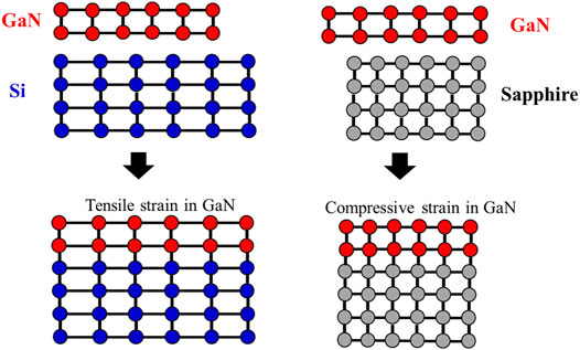
FIGURE 2. The schematic of the lattice difference and the strain for GaN films grown on Si (left) and sapphire (right).
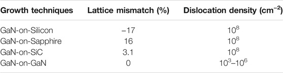
TABLE 1. The comparison of dislocation density of different growth techniques. The lattice mismatch is calculated by (aepi−asub)/asub.
Over the last decade, researchers have spent extensive efforts to develop the free-standing GaN substrates using methods such as hydride vapor-phase epitaxy (HVPE), Ammonothermal, and sodium flux enabling the homogeneous growth of GaN (Fawamura et al., 2006; Paskova and Evans, 2009). The issue of lattice mismatch could be solved by the homogeneous growth on free-standing single-crystalline GaN substrates. The overall quality of the epitaxial GaN was improved remarkably over the last decade, lowering the defect density in the material, making it suitable for impact ionization of carriers. On bulk GaN substrates, lo and behold, the impact ionization and avalanche breakdown were finally reported in p-i-n diodes in 2013 by Avogy Inc. (Disney et al., 2013). Since then, multiple research groups have reported the avalanche breakdown in GaN p-n diodes and extended the capability to Junction Field-Effect Transistors (JFETs) (Kizilyalli et al., 2013; Nomoto et al., 2016; Cao et al., 2018; Maeda et al., 2018; Ji D. et al., 2019; Maeda et al., 2019a; Fukushima et al., 2019; Ohta et al., 2019; Ji et al., 2020a; Ji et al., 2020b; Ji and Chowdhury, 2020; Liu et al., 2020; Liu et al., 2021). Our GaN APDs (Ji et al., 2020b), were also grown on the bulk GaN, which fulfilled the first requirement of high-quality- low defect density (LDD) epitaxial films.
The second requirement for a guaranteed robust avalanche capability is efficient edge termination (Baliga, 2012). An edge termination that can provide extra negative charges to terminate the electric field lines at the device boundary to reduce any localized peak electric field at any surface or corners is important for the realization of an APD. Figure 3 shows several edge terminations that were proposed for avalanche GaN p-n diodes, including the ion implantation-based edge termination (Kizilyalli et al., 2013; Ji et al., 2020a), etch-based edge termination (Fukushima et al., 2019; Maeda et al., 2018), and field-plated edge termination in which the field plate is connected to the anode electrode (Nomoto et al., 2016; Ohta et al., 2019). The schematic of the electric field distribution in the GaN p-n diodes with and without the ion-implanted edge termination is shown in Figure 4. The most common technique to form the mesa and isolation is the dry etching, which could lead to sharp corners and the dense electric field lines around the device, as shown in Figure 4A. Figure 4B shows the schematic of a GaN p-n diode with the ion-implanted moat etch termination (Ji et al., 2020a), where the corners are rounded during isolation and can effectively reduce the localized peak electric field. Moat termination combined with implantation can compensate for the dry etching-induced damages, eliminating the leakage current through the etched surface.
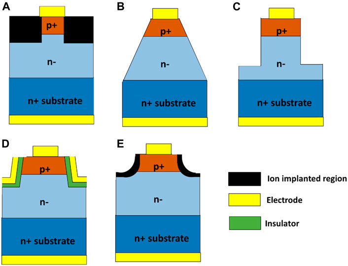
FIGURE 3. Reported edge terminations that enable GaN pn diodes with avalanche capability: (A) ion implanted edge termination (Kizilyalli et al., 2013); (B) bevel etch edge termination (Maeda et al., 2018); (C) deep etch edge termination (Fukushima et al., 2019); (D) field plate edge termination (Nomoto et al., 2016; Ohta et al., 2019); and (E) moat etch edge termination with ion implantation compensation (Ji et al., 2020a).
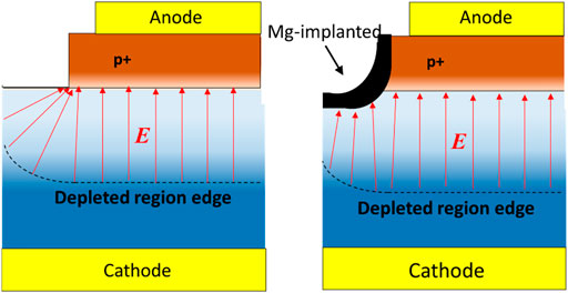
FIGURE 4. The electric field in the reverse-biased p-n diodes: (A) without and (B) with edge termination. To enhance the avalanche robustness, edge terminations are required to enable more uniformly distributed electric fields, which can be indicated by more uniform electric field lines around the device in the figure.
Characterization of Avalanche Breakdown in GaN
The most notable feature with avalanche breakdown in GaN APDs is the positive temperature coefficient of the breakdown voltage. Impact ionization is a process that energy transfers from the energetic carriers to the crystal lattice by scattering. When the temperature is elevated, the crystal lattice vibration becomes stronger, which scatters the carriers more frequently and reduces the impact ionization mean free path. Therefore, it is more difficult for carriers to gain the threshold energy to trigger the impact ionization. Experimental data also indicate that the impact ionization coefficients of both electrons and holes are decreasing when the measurement temperature increases (Ji D. et al., 2019; Maeda et al., 2019b; Cao et al., 2021). Figure 5A shows a temperature-dependent avalanche breakdown characteristics of a GaN APD reported by our group (Ji et al., 2020b). It indicates that the breakdown voltage of the device increases with temperature linearly, as shown in Figure 5B. The temperature-dependent breakdown voltage, BV(T), can be fitted to the following formula:
where BVRT is the breakdown voltage measured in the room temperature, and θ is the temperature coefficient. According to the data presented in Figure 5B, the temperature coefficient, θ, of GaN can be extracted to be 3.85 × 10⁻⁴ (Ji et al., 2020b). Table 2 summarizes the temperature coefficients of various semiconductors (Hall, 1967; Vassilevski et al., 2000; Groves et al., 2003; Tan et al., 2010), it indicates that all the semiconductors have positive temperature coefficients, whose values are in the order of 10−4 K−1. We should note here that the positive temperature coefficient is an extremely important verification of avalanche. This verification is critical in determining if the gain in the APD is due to avalanche or any other mechanism. III-V (e.g GaAs) devices avalanche at a much lower electric field (0.5 MV/cm) and are more routinely observed. The measurement of the positive temperature coefficient is not often reported in III-As APDS (Hu et al., 1996; Anselm et al., 1997), perhaps due to its certainty. However, in GaN, often gain can be witnessed without avalanche, such as in heterojunction-based photodetectors, necessitating the importance of temperature measurements to confirm the avalanche.
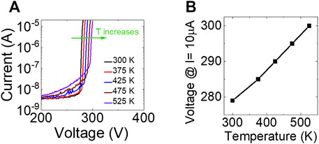
FIGURE 5. (A) Temperature-dependent avalanche breakdown characteristics of a GaN APD; and (B) the breakdown voltage as a function of temperature. The breakdown voltage was defined as the applied voltage that the current reaches 10 µA. This figure is reprinted from AIP Publishing.
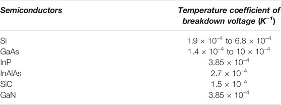
TABLE 2. A summary of temperature coefficient of breakdown voltage of various semiconductors (Hall, 1967; Vassilevski et al., 2000; Groves et al., 2003; Tan et al., 2010; Ji et al., 2020b).
Since GaN is a direct bandgap semiconductor, there are photons generated during the recombination of electrons and holes. When the GaN p-n diode is forward biased, there are electrons and holes injections into the p- and n-regions respectively, therefore an emission in the range of 370–420 nm light can be observed during the recombination of these carriers (Nakamura, 2015). When a reverse bias is applied to a GaN p-n diode and forces the device to an avalanche breakdown, the impact ionization process generates excess electrons and holes in the depletion region and should release photons during the radiative recombination of those carriers. Therefore, a 370–420 nm (violet/blue-violet) electroluminescence is expected to be observed in a GaN APD. This has been observed in GaAs where the 950 nm light is emitted (Lahbabi et al., 2004). Figure 6A presents the optical microscope image of a GaN APD layout. The image of the APD with avalanche induced electroluminescence is shown in Figure 6B (Ji et al., 2020b).
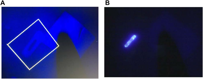
FIGURE 6. (A) The optical microscope image of the APD layout. The APD edges were covered by metal, leaving a rectangular via to detect optical signals. (B) the image of the APD when the avalanche occurred, the light was emitted from the device.
Impact Ionization Coefficients
In GaN APDs, the impact ionization multiplication can be written as a function of impact ionization coefficients:
And
Where Mn is the electron-initiated multiplication factor and Mp is the hole-initiated multiplication factor, W is the width of the depletion region. The electron-initiated impact ionization multiplication is illustrated in Figure 7A, where UV light illuminates the p-GaN region and the photogenerated electrons are drift into the depletion region and initiate the impact ionization process. Figure 7B shows the hole-initiated impact ionization multiplication, where UV light illuminates the n-GaN layer and photogenerated holes initiate the impact ionization process.
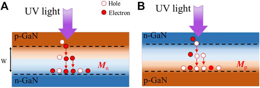
FIGURE 7. The schematic illustration of the (A) electron- and (B) hole-initiated impact ionization multiplication in GaN p-n junctions.
For GaN APDs, the performance, such as gain and excess noise, depends on the impact ionization coefficients of both electrons and holes (Sze and Ng, 2006). Therefore, it is important to measure the impact ionization coefficients in GaN.
The reported estimated ionization coefficients in GaN are listed in Table 3 and are plotted in Figure 8.

TABLE 3. Estimated impact ionization coefficients in GaN.
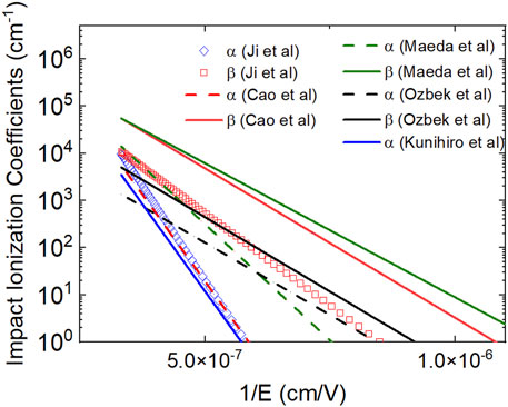
FIGURE 8. Reported impact ionization coefficients of electrons (α) and holes (β) in GaN (Kunihiro et al., 1999; Özbek, 2012; Ji D. et al., 2019; Maeda et al., 2019a; Cao et al., 2021).
The studies reflected in Figure 8, helps us realize that within the reasonably high electric field range (1 MV/cm—3 MV/cm), holes have a larger impact ionization coefficient compared to electrons in GaN, the hole-initiated multiplication APDs should have better performance compared to electron-initiated multiplication APDs, and this has been proved both theoretically and experimentally (McClintock et al., 2007; Minder et al., 2007; Zheng et al., 2016).
A Survey of GaN-Based Avalanche Photodiode Structures
The early GaN APD studies belonged to electron-initiated devices where the structures were based on GaN-on-Sapphire (Verghese et al., 1998; Carrano et al., 2000; Cicek et al., 2010; Sun et al., 2010), as shown in Figure 9A. Large defect density, as well as the etching-induced damages, contributed significantly to the high dark current density, which is in the range of 10–4 to 1 A/cm2 (Verghese et al., 1998; Carrano et al., 2000; Cicek et al., 2010; Sun et al., 2010). With the introduction of GaN-on-GaN APDs, as shown in Figure 9B, dark current density of less than 10–4 A/cm2 could be realized, along with a gain of 104 (Limb et al., 2006; Shen et al., 2007; Yoo et al., 2007; Zhang et al., 2008; Zhang et al., 2009).
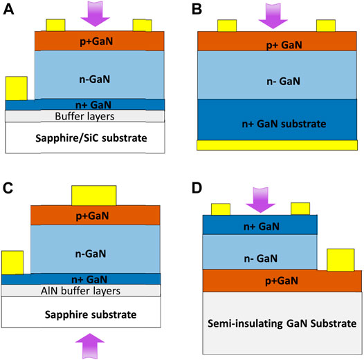
FIGURE 9. The reported GaN APD structures: (A) front-illuminated electron-initiated APDs on sapphire or SiC substrates; (B) front-illuminated electron-initiated APDs on free-standing GaN substrates; (C) back-illuminated hole-initiated APDs based on sapphire substrates, and (D) front-illuminated hole-initiated APDs based on free-standing GaN substrates.
Because the hole’s impact ionization coefficient is much larger than the electron’s in GaN, the hole-initiated APDs are more attractive due to the low excess noise factor and high gain (Zheng et al., 2016; McClintock et al., 2007; Minder et al., 2007). Therefore, backside-illuminated GaN-on-Sapphire APDs (p-type on top) were proposed and fabricated (McClintock et al., 2007; Minder et al., 2007), as shown in Figure 9C. Although the backside-illuminated GaN-on-Sapphire APDs achieved remarkable performance compared to the topside (aka frontside)-illuminated electron-initiated APDs, the backside-illuminated APDs structures will face challenges when transferred from its free-standing GaN substrate. An alternative path was attempted with a buried p-GaN layer. Ionization of acceptors in buried p-GaN layers remains to be a challenge in GaN. Mg is a deep acceptor in GaN with an energy difference of 0.17 eV from the valence band. When doped, about 1% Mg is active to provide free holes in the system. Innovative methods have increased this activation to 10% (Smorchkova et al., 2000; Nakayaa et al., 1996) and created more efficient p-n junctions. It has been vastly studied, that during the MOCVD growth, the Mg dopants in the p-GaN are compensated by H, forming the Mg-H complex (Nakamura et al., 1992a; Nakamura et al., 1992b). If the Mg-doped GaN is buried beneath the n-GaN, because of the limited H diffusion in n-GaN (Czernecki et al., 2018), Mg dopants cannot be activated. To activate the buried Mg-doped GaN, one must etch through the n-GaN layers, exposing the p-GaN to the atmosphere (Li et al., 2018; Narita et al., 2018). Figure 9D presents an n-p structure grown on a GaN substrate reported by Ji et al. (2020b), which is good for topside illumination hole-initiated APDs.
To enhance the pure hole-injection, the separated absorption and multiplication (SAM) design was utilized. In the regular p-i-n structure, the mixed-mode injection can be caused by the absorption of light in the multiplication layer, which may affect the device’s gain and noise. Therefore, by adding a charge layer to separate the absorption and multiplication layers is an effective way to enhance the gain and reduce noise. Figure 10A shows the schematic of a backside illuminated SAM APD structure (McClintock et al., 2009; Zheng et al., 2012; Wang et al., 2014; Shao et al., 2017; Ji et al., 2018; Zhang et al., 2020), and the corresponding electric field distribution along the depletion region. By inserting a Si-doped charge layer to separate the absorption and multiplication layers, the electric field in the absorption layer remains low that avalanche multiplication cannot be triggered in the absorption layer, while the electric field in the multiplication layer remains high where the avalanche can occur. Multiple groups have reported the structure shown in Figure 10A, however, the backside-illumination configuration cannot be achieved with bulk GaN substrates.
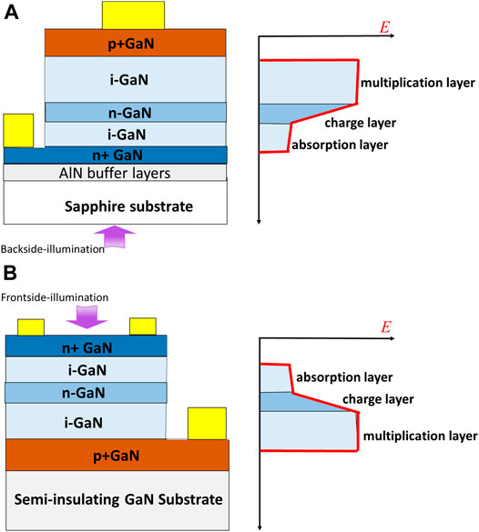
FIGURE 10. (A) The separated absorption and multiplication (SAM) structure based on GaN-on-Sapphire (left) and the corresponding electric field distribution along the vertical direction (right). (B) the proposed SAM structure based on GaN-on-GaN (left) and the corresponding electric field along the vertical direction (right).
Figure 10B highlights a proposed SAM APD structure based on bulk GaN substrates, which is modified from our prior reported structure (Ji et al., 2020b). The structure includes a separated absorption and multiplication layers on top of a buried p-GaN layer. The corresponding electric field distribution is also shown in Figure 10B. Compared to the reported GaN APD structures, the structure shown in Figure 10B has three advantages: 1) homoepitaxial growth using bulk GaN substate; 2) the hole-initiation; and 3) the SAM structure. These combinations show a great potential for producing high-sensitivity UV detectors.
One other important feature of GaN-based APD is its high-temperature tolerance. Because of the wide bandgap, the intrinsic carrier density of GaN, which is proportional to
Last but not least, compared to the photoconductor and phototransistor, p-i-n based photodetectors have the fastest response time, which is determined by three factors: 1) the diffusion time of carriers before they enter the depletion region, 2) the transient time through the depletion region, and 3) the RLCp-i-n time delay, where RL is the load resistance, and the Cp-i-n is the junction capacitance. To minimize the response time, the n-GaN layer thickness should be minimized for the hole-initiated APD, and the p-GaN layer thickness should be minimized for the electron-initiated APD. Additionally, the device should be well designed to minimize the junction capacitance. Table 4 summarizes the reported response time of various GaN photodetectors, it indicates that GaN p-i-n diode and APD have the fastest response speed compared to other types of devices, enabling a short response time of 10–8 s.

TABLE 4. Response times of various GaN based photodetectors.
The reported GaN APD structures and performances are summarized in Table 5, which suggests that hole-initiated APD on GaN substrate enabled a record responsivity up to 60 A/W. This result has sparked interest in weak UV light detections.
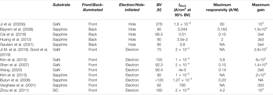
TABLE 5. Summary of the reported key results on GaN avalanche photodiodes.
Summary
In this article, we attempted to shed some light on GaN avalanche photodiodes for UV detection and the possibilities, which are of growing interest. GaN APDs are naturally suited to serve application that requires high temperature/harsh environment tolerance. The design space of GaN APDs was reviewed. It is quite clear from prior reports that a robust avalanche capability in GaN APDs are the result of at least two key requirements are discussed: 1) LDD in the epitaxial layers to offer the travel distance for the carriers to establish an avalanche process; and 2) optimized edge termination that can eliminate the localized peak electric field around the device edges. In the context of APD performance, we discussed the importance of the positive temperature coefficient of breakdown voltage, as well as the observation of avalanche-induced electroluminescence that ensures the gain mechanism is reliable. In addition, GaN’s impact ionization coefficients were discussed to highlight the scope of GaN APDs in applications. Since the ratio of hole’s and electron’s impact ionization coefficients (β/α) is so large, the hole-initiated GaN APDs with buried p-GaN layer are more attractive due to the low excess noise and high gain.
Author Contributions
DJ and SC proposed the idea, collected data, and wrote the article.
Conflict of Interest
The authors declare that the research was conducted in the absence of any commercial or financial relationships that could be construed as a potential conflict of interest.
Publisher’s Note
All claims expressed in this article are solely those of the authors and do not necessarily represent those of their affiliated organizations, or those of the publisher, the editors and the reviewers. Any product that may be evaluated in this article, or claim that may be made by its manufacturer, is not guaranteed or endorsed by the publisher.
References
Amano, H. (2015). Nobel Lecture: Growth of GaN on Sapphire via Low-Temperature Deposited Buffer Layer and Realization of P -type GaN by Mg Doping Followed by Low-Energy Electron Beam Irradiation. Rev. Mod. Phys. 87, 1133–1138. doi:10.1103/revmodphys.87.1133
Anselm, K. A., Yuan, P., Hu, C., Lenox, C., Nie, H., Kinsey, G., et al. (1997). Characteristics of GaAs and AlGaAs Homojunction Avalanche Photodiodes with Thin Multiplication Regions. Appl. Phys. Lett. 71, 3883–3885. doi:10.1063/1.120533
Baliga, B. J. (2012). Fundamentals of Power Semiconductor Devices. New York: Springer Science + Business Media LLC. Chapter 3.
Bayram, C., Pau, J. L., McClintock, R., Razeghi, M., Ulmer, M. P., and Silversmith, D. (2008). High Quantum Efficiency Back-Illuminated GaN Avalanche Photodiodes. Appl. Phys. Lett. 93, 211107. doi:10.1063/1.3039061
Butun, B., Tut, T., Ulker, E., Yelboga, T., and Ozbay, E. (2008). High-performance Visible-Blind GaN-based P-I-N Photodetectors. Appl. Phys. Lett. 92, 033507. doi:10.1063/1.2837645
Cai, Q., Luo, W. K., Li, Q., Li, M., Chen, D. J., Lu, H., et al. (2018). AlGaN Ultraviolet Avalanche Photodiodes Based on a Triple-mesa Structure. Appl. Phys. Lett. 113, 123503. doi:10.1063/1.5049621
Cao, L., Wang, J., Harden, G., Ye, H., Stillwell, R., Hoffman, A. J., et al. (2018). Experimental Characterization of Impact Ionization Coefficients for Electrons and Holes in GaN Grown on Bulk GaN Substrates. Appl. Phys. Lett. 112, 262103. doi:10.1063/1.5031785
Cao, L., Zhu, Z., Harden, G., Ye, H., Wang, J., Hoffman, A., et al. (2021). Temperature Dependence of Electron and Hole Impact Ionization Coefficients in GaN. IEEE Trans. Electron. Devices 68, 1228–1234. doi:10.1109/ted.2021.3054355
Carrano, J. C., Lambert, D. J. H., Eiting, C. J., Collins, C. J., Li, T., Wang, S., et al. (2000). GaN Avalanche Photodiodes. Appl. Phys. Lett. 76, 924–926. doi:10.1063/1.125631
Cicek, E., Vashaei, Z., McClintock, R., Bayram, C., and Razeghi, M. (2010). Geiger-mode Operation of Ultraviolet Avalanche Photodiodes Grown on Sapphire and Free-Standing GaN Substrates. Appl. Phys. Lett. 96, 261107. doi:10.1063/1.3457783
Czernecki, R., Grzanka, E., Jakiela, R., Grzanka, S., Skierbiszewski, C., Turski, H., et al. (2018). Hydrogen Diffusion in GaN:Mg and GaN:Si. J. Alloys Comp. 747, 354–358. doi:10.1016/j.jallcom.2018.02.270
Disney, D., Nie, H., Edward, A., Bour, D., Shah, H., and Kizilyalli, I. C. (2013). “Vertical Power Diodes in Bulk GaN,” in 2013 25th International Symposium on Power Semiconductor Devices IC’s (ISPSD) (Kanazawa, Japan: IEEE), 59–62.
Fawamura, F., Umeda, H., Morishita, M., Kawahara, M., Yoshimura, M., Mori, Y., et al. (2006). Growth of a Large GaN Single Crystal Using the Liquid Phase Epitaxy (LPE) Technique. Jpn. J. Appl. Phys. 45, L1136. doi:10.1143/JJAP.42.L4
Fukushima, H., Usami, S., Ogura, M., Ando, Y., Tanaka, A., Deki, M., et al. (2019). Deeply and Vertically Etched butte Structure of Vertical GaN P–N Diode with Avalanche Capability. Jpn. J. Appl. Phys. 12, SCCD25. doi:10.7567/1347-4065/ab106c
Gautam, L., Jaud, A. G., Lee, J., Brown, G. J., and Razeghi, M. (2021). Geiger-Mode Operation of AlGaN Avalanche Photodiodes at 255 Nm. IEEE J. Quan. Electro. 57 (2), 4500106.
Groves, C., Ghin, R., David, J. P. R., and Rees, G. J. (2003). Temperature Dependence of Impact Ionization in GaAs. IEEE Trans. Electron. Devices 50, 2027–2031. doi:10.1109/ted.2003.816918
Guo, D., Su, Y., Shi, H., Li, P., Zhao, N., Ye, J., et al. (2018). Self-Powered Ultraviolet Photodetector with Superhigh Photoresponsivity (3.05 A/W) Based on the GaN/Sn:Ga2O3 Pn Junction. ACS Nano 12, 12827–12835. doi:10.1021/acsnano.8b07997
Hadfield, R. H. (2009). Single-photon Detectors for Optical Quantum Information Applications. Nat. Photon 3, 696–705. doi:10.1038/nphoton.2009.230
Hall, R. (1967). Temperature Coefficient of the Breakdown Voltage of Silicon P-N Junctions†. Int. J. Electro. 22, 513–519. doi:10.1080/00207216708937986
Hu, C., Anselm, K. A., Streetman, B. G., and Campbell, J. C. (1996). Noise Characteristics of Thin Multiplication Region GaAs Avalanche Photodiodes. Appl. Phys. Lett. 69, 3734–3736. doi:10.1063/1.117205
Hu, J. (2008). 4H-SiC Detectors for Low Level Ultraviolet Detection (New Jersey: Rutgers, The State University of New Jersey). PhD. Dissertation.
Huang, Y., Chen, D. J., Lu, H., Dong, K. X., Zhang, R., Zheng, Y. D., et al. (2012). Back-illuminated Separate Absorption and Multiplication AlGaN Solar-Blind Avalanche Photodiodes. Appl. Phys. Lett. 101, 253516. doi:10.1063/1.4772984
Ji, D., and Chowdhury, S. (2020). On Impact Ionization and Avalanche in Gallium Nitride. Appl. Phys. Lett. 117, 252107. doi:10.1063/5.0031504
Ji, D., Ercan, B., Benson, G., Newaz, A. K. M., and Chowdhury, S. (2020b). 60 A/W High Voltage GaN Avalanche Photodiode Demonstrating Robust Avalanche and High Gain up to 525 K. Appl. Phys. Lett. 116, 211102. doi:10.1063/1.5140005
Ji, D., Ercan, B., and Chowdhury, S. (2019). Experimental Determination of Impact Ionization Coefficients of Electrons and Holes in Gallium Nitride Using Homojunction Structures. Appl. Phys. Lett. 115, 073503. doi:10.1063/1.5099245
Ji, D., Li, S., Ercan, B., Ren, C., and Chowdhury, S. (2020a). Design and Fabrication of Ion-Implanted Moat Etch Termination Resulting in 0.7 m$\Omega\cdot$ Cm2/1500 V GaN Diodes. IEEE Electron. Device Lett. 41 (2), 264–267. doi:10.1109/led.2019.2960349
Ji, M.-H., Kim, J., Detchprohm, T., Zhu, Y., Shen, S.-C., and Dupuis, R. D. (2018). p-i-p-i-n Separate Absorption and Multiplication Ultraviolet Avalanche Photodiodes. IEEE Photon. Technol. Lett. 30 (2), 181–184. doi:10.1109/lpt.2017.2779798
Ji, M., Jeong, H., Bakhtiary-Noodeh, M., Shen, S.-C., Detchprohm, T., Sood, A. K., et al. (2019). “Gallium Nitride Materials and Devices XIV,” in Proc. SPIE (San Francisco, CA: SPIE), 10918.
Kim, J., Ji, M., Detchprohm, T., Dupuis, R., Ryou, J., Sood, A. K., et al. (2015). Comparison of AlGaN P–I–N Ultraviolet Avalanche Photodiodes Grown on Free-Standing GaN and Sapphire Substrates. Appl. Phys. Exp. 8, 122202. doi:10.7567/APEX.8.122202
Kizilyalli, I. C., Edwards, A. P., Nie, H., Disney, D., and Bour, D. (2013). High Voltage Vertical GaN P-N Diodes with Avalanche Capability. IEEE Trans. Electron. Devices 60, 3067–3070. doi:10.1109/ted.2013.2266664
Krost, A., and Dadgar, A. (2002). GaN-based Optoelectronics on Silicon Substrates. Mater. Sci. Eng. B 93 (97), 77–84. doi:10.1016/s0921-5107(02)00043-0
Kunihiro, K., Kasahara, K., Takahashi, Y., and Ohno, Y. (1999). Experimental Evaluation of Impact Ionization Coefficients in GaN. IEEE Electron. Device Lett. 20 (12), 608–610. doi:10.1109/55.806100
Lahbabi, M., Ahaitouf, A., Fliyou, M., Abarkan, E., Jean-Pierre, C., Bath, A., et al. (2004). Analysis of Electroluminescence Spectra of Silicon and Gallium Arsenide P-N junction in Avalanche Breakdown. J. Appl. Phys. 95, 1822–1828. doi:10.1063/1.1643188
Li, P., Shi, H., Chen, K., Guo, D., Cui, W., Zhi, Y., et al. (2017). Construction of GaN/Ga2O3 P-N junction for an Extremely High Responsivity Self-Powered UV Photodetector. J. Mater. Chem. C 5, 10562–10570. doi:10.1039/c7tc03746e
Li, W., Nomoto, K., Lee, K., Islam, S. M., Hu, Z., Zhu, M., et al. (2018). Activation of Buried P-GaN in MOCVD-Regrown Vertical Structures. Appl. Phys. Lett. 113, 062105. doi:10.1063/1.5041879
Limb, J. B., Yoo, D., Ryou, J. H., Lee, W., Shen, S. C., Dupuis, R. D., et al. (2006). GaN Ultraviolet Avalanche Photodiodes with Optical Gain Greater Than 1000 Grown on GaN Substrates by Metal-Organic Chemical Vapor Deposition. Appl. Phys. Lett. 89, 11112. doi:10.1063/1.2219390
Liu, J., Xiao, M., Zhang, R., Pidaparthi, S., Cui, H., Edwards, A., et al. (2021). 1.2-kV Vertical GaN Fin-JFETs: High-Temperature Characteristics and Avalanche Capability. IEEE Trans. Electron. Devices 68, 2025–2032. doi:10.1109/ted.2021.3059192
Liu, J., Xiao, M., Zhang, R., Pidaparthi, S., Drowley, C., Baubutr, L., et al. (2020). Trap-Mediated Avalanche in Large-Area 1.2 kV Vertical GaN P-N Diodes. IEEE Electron. Device Lett. 41 (9), 1328–1331. doi:10.1109/led.2020.3010784
Liu, L., and Edgar, J. H. (2002). Substrates for Gallium Nitride Epitaxy. Mater. Sci. Eng. R: Rep. 37, 61–127. doi:10.1016/s0927-796x(02)00008-6
Maeda, T., Narita, T., Ueda, H., Kanechika, M., Uesugi, T., Kachi, T., et al. (2018). Proceedings of IEEE International Electron Devices Meeting (IEDM). San Francisco, CA: IEEE, 689–693.
Maeda, T., Narita, T., Ueda, H., Kanechika, M., Uesugi, T., Kachi, T., et al. (2019b). Measurement of Avalanche Multiplication Utilizing Franz-Keldysh Effect in GaN P-N junction Diodes with Double-Side-Depleted Shallow Bevel Termination. Appl. Phys. Lett. 115, 142101. doi:10.1063/1.5114844
Maeda, T., Narita, T., Yamada, S., Kachi, T., Kimoto, T., Horita, M., et al. (2019a). IEEE International Electron Devices Meeting (IEDM). Shanghai, China: IEEE, 4.2.1–4.2.4.
McClintock, R., Pau, J. L., Minder, K., Bayram, C., Kung, P., and Razeghi, M. (2007). Hole-initiated Multiplication in Back-Illuminated GaN Avalanche Photodiodes. Appl. Phys. Lett. 90, 141112. doi:10.1063/1.2720712
McClintock, R., Pau, J. L., Minder, K., Bayram, C., and Razeghi, M. (2009). “III-nitride Photon Counting Avalanche Photodiodes,” in Proc. of SPIE. San Jose, CA: SPIE, 69000N–69003N.6900
Minder, K., Pau, J. L., McClintock, R., Kung, P., Bayram, C., Razeghi, M., et al. (2007). Scaling in Back-Illuminated GaN Avalanche Photodiodes. Appl. Phys. Lett. 91, 073513. doi:10.1063/1.2772199
Mion, C., Muth, J. F., Preble, E. A., and Hanser, D. (2006). Accurate Dependence of Gallium Nitride thermal Conductivity on Dislocation Density. Appl. Phys. Lett. 89, 092123. doi:10.1063/1.2335972
Nakamura, S., Iwasa, N., Senoh, M., and Mukai, T. (1992a). Hole Compensation Mechanism of P-type GaN Films. Jpn. J. Appl. Phys. Part. 1 31 (5A), 1258–1266. doi:10.1143/jjap.31.1258
Nakamura, S., Mukai, T., and Senoh, M. (1992b). Thermal Annealing Effects on P-type Mg-Doped GaN Films. Jpn. J. Appl. Phys. Part. 2 31 (2B), L139–L142. doi:10.1143/jjap.31.l139
Nakamura, S. (2015). Nobel Lecture: Background story of the Invention of Efficient Blue InGaN Light Emitting Diodes. Rev. Mod. Phys. 87, 1139–1151. doi:10.1103/revmodphys.87.1139
Nakayaa, H., Hacke, P., and Khan, M. R. H. (1996). Electrical Transport Properties of P-GaN. Jpn. J. Appl. Phys. 35, L282–L284.
Narita, T., Tomita, K., Yamada, S., and Kachi, T. (2018). Quantitative Investigation of the Lateral Diffusion of Hydrogen in P-type GaN Layers Having NPN Structures. Appl. Phys. Express 12, 011006. doi:10.7567/1882-0786/aaf418
Nomoto, K., Song, B., Hu, Z., Zhu, M., Qi, M., Kaneda, N., et al. (2016). 1.7-kV and 0.55-$\text{m}\Omega \cdot \text {cm}^{2}$ GaN P-N Diodes on Bulk GaN Substrates with Avalanche Capability. IEEE Electron. Device Lett. 37 (2), 161–164. doi:10.1109/led.2015.2506638
Ohta, H., Asai, N., Horikiri, F., Narita, Y., Yoshida, T., and Mishima, T. (2019). 4.9 kV Breakdown Voltage Vertical GaN P–N junction Diodes with High Avalanche Capability. Jpn. J. Appl. Phys. 58, SCCD03. doi:10.7567/1347-4065/ab0cfa
Osinsky, A., Gangopadhyay, S., Gaska, R., Williams, B., Khan, M. A., Kuksenkov, D., et al. (1997). Low Noisep-π-nGaN Ultraviolet Photodetectors. Appl. Phys. Lett. 71, 2334–2336. doi:10.1063/1.120023
Özbek, A. M. (2012). Measurement of Impact Ionization Coefficients in GaN (North Carolina State University). Ph.D. Dissertation.
Paskova, T., and Evans, K. R. (2009). GaN Substrates-Progress, Status, and Prospects. IEEE J. Select. Top. Quan. Electron. 15, 1041–1052. doi:10.1109/jstqe.2009.2015057
Qiu, X., Song, Z., Sun, L., Zhang, Z., Lv, Z., Wen, Q., et al. (2020). High-gain AlGaN/GaN Visible-Blind Avalanche Heterojunction Phototransistors. J. Mater. Sci. Mater. Electron. 31, 652–657. doi:10.1007/s10854-019-02571-8
Satterthwaite, P. F., Yalamarthy, A. S., Scandrette, N. A., Newaz, A. K. M., and Senesky, D. G. (2018). High Responsivity, Low Dark Current Ultraviolet Photodetectors Based on Two-Dimensional Electron Gas Interdigitated Transducers. ACS Photon. 5, 4277–4282. doi:10.1021/acsphotonics.8b01169
Shao, Z. G., Yang, X. F., You, H. F., Chen, D. J., Lu, H., Zhang, R., et al. (2017). Ionization-Enhanced AlGaN Heterostructure Avalanche Photodiodes. IEEE Electron. Device Lett. 38 (4), 485–488. doi:10.1109/led.2017.2664079
Shen, S.-C., Yun Zhang, Y., Dongwon Yoo, D., Jae-Boum Limb, J.-B., Jae-Hyun Ryou, J.-H., Yoder, P. D., et al. (2007). Performance of Deep Ultraviolet GaN Avalanche Photodiodes Grown by MOCVD. IEEE Photon. Technol. Lett. 19, 1744–1746. doi:10.1109/lpt.2007.906052
Smorchkova, I. P., Haus, E., Heying, B., Kozodoy, P., Fini, P., Ibbetson, J. P., et al. (2000). Mg Doping of GaN Layers Grown by Plasma-Assisted Molecular-Beam Epitaxy. Appl. Phys. Lett. 76, 718–720. doi:10.1063/1.125872
Sood, A. K., Zeller, J. W., Ghuman, P., Babu, S., Dhar, N. K., Ganguly, S., et al. (2019). “Sensors, Systems and Next-Generation Satellites XXIII,” in Proceedings of SPIE 11151 (Strasbourg, France: SPIE), 1115113.
Sun, L., Chen, J., Li, J., and Jiang, H. (2010). AlGaN Solar-Blind Avalanche Photodiodes with High Multiplication Gain. Appl. Phys. Lett. 97, 191103. doi:10.1063/1.3515903
Sun, X., Wu, C., Wang, Y., and Guo, D. (2022). Photoinduced Carrier Transport Mechanism in Pn- and nn-GaN/GaON Heterojunctions. J. Vacuum Sci. Techn. B 40, 012204. doi:10.1116/6.0001601
Sze, S. M., and Ng, K. K. (2006). Physics of Semiconductor Devices. Hoboken: John Wiley and Sons, Inc. Chapter 13.
Tan, L. J. J., Ong, D. S. G., Ng, J. S., Tan, C. H., Jones, S. K., Qian, Y., et al. (2010). Temperature Dependence of Avalanche Breakdown in InP and InAlAs. IEEE J. Quan. Electron. 46, 1153–1157. doi:10.1109/jqe.2010.2044370
Vassilevski, K. V., Zekentes, K., Zorenko, A. V., and Romanov, L. P. (2000). Experimental Determination of Electron Drift Velocity in 4H-SiC P/sup +/-N-N/sup +/Avalanche Diodes. IEEE Electron. Device Lett. 21, 485–487. doi:10.1109/55.870609
Verghese, S., McIntosh, K. A., Molnar, R. J., Mahoney, L. J., Aggarwal, R. L., Geis, M. W., et al. (2001). GaN Avalanche Photodiodes Operating in Linear-Gain Mode and Geiger Mode. IEEE Trans. Electron. Devices 48 (3), 502–511. doi:10.1109/16.906443
Verghese, S., Mclntosh, K. A., Molnar, R. J., Chen, C.-L., Molvar, K. M., Melngailis, I., et al. (1998). Device Research Conference. Charlottesville, VA: IEEE, 54–55.
Wang, W. (2020). Uniform and High Gain GaN P-I-N Ultraviolet APDs Enabled by Beveled-Mesa Edge Termination. IEEE Photon. Technol. Lett. 32 (21), 1357–1360. doi:10.1109/lpt.2020.3025290
Wang, X., Hu, W., Pan, M., Hou, L., Xie, W., Xu, J., et al. (2014). Study of Gain and Photoresponse Characteristics for Back-Illuminated Separate Absorption and Multiplication GaN Avalanche Photodiodes. J. Appl. Phys. 115 (1), 013103. doi:10.1063/1.4861148
Wang, Y., Zhang, Y., Yang, Y. A., Lu, X., and Zou, X. (2020). Simulation Study of Front-Illuminated GaN Avalanche Photodiodes with Hole-Initiated Multiplication. Cogent Eng. 7, 1764171. doi:10.1080/23311916.2020.1764171
Xu, G. Y., Salvador, A., Kim, W., Fan, Z., Lu, C., Tang, H., et al. (1997). High Speed, Low Noise Ultraviolet Photodetectors Based on GaN P-I-N and AlGaN(p)-GaN(i)-GaN(n)structures. Appl. Phys. Lett. 71, 2154–2156. doi:10.1063/1.119366
Yeh, P. S., Chiu, Y.-C., Wu, T.-C., Chen, Y.-X., Wang, T.-H., and Chou, T.-C. (2019). Monolithic Integration of GaN-based Phototransistors and Light-Emitting Diodes. Opt. Express 27, 29854. doi:10.1364/oe.27.029854
Yoo, D., Limb, J., Ryou, J.-H., Zhang, Y., Shen, S.-C., Dupuis, R. D., et al. (2007). Al$_{x}$Ga$_{1-x}$N Ultraviolet Avalanche Photodiodes Grown on GaN Substrates. IEEE Photon. Technol. Lett. 19, 1313–1315. doi:10.1109/lpt.2007.902376
Zhang, Y. (2011). Development of III-Nitride Bipolar Devices: Avalanche Photodiodes, Laser Diodes, and Double-Heterojunction Bipolar Transistors (Georgia Institute of Technology). PhD Dissertation.
Zhang, Y., Shen, S.-C., Kim, H. J., Choi, S., Ryou, J.-H., Dupuis, R. D., et al. (2009). Low-noise GaN Ultraviolet P-I-N Photodiodes on GaN Substrates. Appl. Phys. Lett. 94, 221109. doi:10.1063/1.3148812
Zhang, Y., Yoo, D., Limb, J.-B., Ryou, J.-H., Dupuis, R. D., and Shen, S.-C. (2008). GaN Ultraviolet Avalanche Photodiodes Fabricated on Free-Standing Bulk GaN Substrates. Phys. Stat. Sol. (C) 5, 2290–2292. doi:10.1002/pssc.200778704
Zhang, Z., Sun, L., Chen, M., Qiu, X., Li, B., and Jiang, H. (2020). Separate Absorption and Multiplication AlGaN Solar-Blind Avalanche Photodiodes with High-Low-Doped and Heterostructured Charge Layer. J. Elec Materi 49 (4), 2343–2348. doi:10.1007/s11664-020-07950-0
Zheng, J.-Y., Wang, L., Hao, Z.-B., Luo, Y., Wang, L.-X., and Chen, X.-K. (2012). A GaN P-I-P-I-N Ultraviolet Avalanche Photodiode. Chin. Phys. Lett. 29 (9), 097804. doi:10.1088/0256-307x/29/9/097804
Zheng, J., Wang, L., Hao, Z., and Luo, Y. (2016). Proc. URSI General Assembly and Scientific Symposium. Beijing, China: IEEE.
Zheng, W., Jia, L., and Huang, F. (2020). Vacuum-Ultraviolet Photon Detections. iScience 23 (6), 101145. doi:10.1016/j.isci.2020.101145
Keywords: GaN, photodiode, APD, UV detector, P-i-n diode
Citation: Ji D and Chowdhury S (2022) On the Scope of GaN-Based Avalanche Photodiodes for Various Ultraviolet-Based Applications. Front. Mater. 9:846418. doi: 10.3389/fmats.2022.846418
Received: 31 December 2021; Accepted: 10 February 2022;
Published: 11 March 2022.
Edited by:
Longxing Su, ShanghaiTech University, ChinaCopyright © 2022 Ji and Chowdhury. This is an open-access article distributed under the terms of the Creative Commons Attribution License (CC BY). The use, distribution or reproduction in other forums is permitted, provided the original author(s) and the copyright owner(s) are credited and that the original publication in this journal is cited, in accordance with accepted academic practice. No use, distribution or reproduction is permitted which does not comply with these terms.
*Correspondence: Srabanti Chowdhury, c3JhYmFudGlAc3RhbmZvcmQuZWR1