 Qiushi Li1†
 Xiaotong Li
 Fan Ding
 Cong Chen
 Shiyi Xiao
- 1Key Laboratory of Specialty Fiber Optics and Optical Access Networks, Joint International Research Laboratory of Specialty Fiber Optics and Advanced Communication, Shanghai Institute for Advanced Communication and Data Science, Shanghai University, Shanghai, China
- 2China Ship Development and Design Center, Wuhan, China
- 3School of Electronic Information, Wuhan University, Wuhan, China
- 4Department of Electrical and Electronic Engineering, Southern University of Science and Technology, Shenzhen, China
Frequency-selective rasorbers (FSRs), which have absorptive and transmissive properties at different frequencies, are crucial in a wide range of applications in communication and radar engineering. However, the FSRs currently available usually exhibit a single high-performance transmission band, which cannot meet the rising demands for modern multiband communication/radar systems. In this article, we propose a dual-band frequency-selective rasorber that utilizes a cascaded metasurface and is designed with an equivalent circuit model and parameter optimization. In addition, a prototype dual-band frequency-selective rasorber is fabricated and characterized. Microwave measurements present two highly transparent peaks located near 11.5 and 17.5 GHz with an insertion loss of around 0.5 dB. Also, there are two absorption bands with absorptivities higher than 80% at 3.9–10.2 GHz and 13–15 GHz. Such low insertion loss for both transparent bands is achieved by optimizing the position of resistors through mode analysis. Our approach facilitates the manufacture of high-performance multi-band frequency-selective rasorbers for use in multi-band communication systems.
1 Introduction
Frequency-selective rasorbers (FSRs) exhibit extraordinary electromagnetic (EM) responses since they are transparent in certain frequency bands while absorptive in others. Such devices have attracted much attention over the last few decades due to both scientific curiosity and potential practical applications (Munk, 2000). For instance, FSRs can be employed as antenna radomes to enhance electromagnetic compatibility for different antenna systems and reduce the antenna radar cross-section (RCS) outside the transmission band. The basic design principle for such frequency-selective rasorbers is to substitute the ground plane of a broadband absorber with a frequency-selective surface to enable the transmission window while maintaining out-of-band absorption properties (Munk, 2009). A critical issue frequently encountered during the design process is ensuring optimal broadband absorptive performance while maintaining high transmission in the communication band.
In the early years, researchers directly integrated the low-pass characteristics of strip-type frequency-selective surfaces with broadband absorbers to fabricate low-pass-type frequency-selective rasorbers (Costa and Monorchio, 2012; Chen et al., 2015; Yu et at., 2017). Because low-frequency waves tend to have superior penetration capability under similar conditions, such low-pass-type frequency-selective rasorbers exhibit low insertion loss within the transmission band associated with a wide absorption band. However, this strategy cannot be directly extended to higher communication bands due to the inherent problem that these broadband absorbers are not naturally transparent at communication frequencies. Recently, the rapid development of metasurface research has paved the way to realize such novel EM devices. Metasurfaces are ultrathin metamaterials that consist of planar microstructures with tailored EM properties. They have a strong ability to control EM waves and exhibit many unique properties that can be applied to functional devices (Yu et al., 2011; Mishra et al., 2017; Xiao et al., 2017; He et al., 2018; Sun et al., 2019). Some examples include anomalous reflection/refraction (Xu et al., 2016; Cao et al., 2019; Akram et al., 2020; Cai et al., 2020; Cai et al., 2021; Ran et al., 2022), vortex beam generators (Zhang et al., 2017; Ma et al., 2020; Li et al., 2022; Wu et al., 2022), surface wave couplers (Sun, et al., 2012; Xiao et al., 2015), and holograms and cloaking (Cai et al., 2015; Xu et al., 2021; Zhen et al., 2021). More recently, researchers have combined completely different EM responses, such as high transmittance and ideal absorption, into single ultrathin cascaded metasurfaces (Pfeoffer and Grbic, 2013; Arbabi et al., 2017). These advances have provided frequency-selective rasorbers with flexibly designed transmission bands, where the core strategy is to use EM resonance to tunnel EM waves through a highly absorptive background (Zhou et al., 2005; Guo et al., 2018; Yang et al., 2019). However, available frequency-selective rasorbers usually only exhibit single high-performance transparent bands (Wang et al., 2018; Guo et al., 2019; Guo et al., 2020; Parameswaran et al., 2021; Yang et al., 2022) or multiple transparent bands with relatively high insertion loss, typically >1 dB (Guo et al., 2019; Guo et al., 2019; Xiu et al., 2020; Sharma et al., 2022). Therefore, high-performance multi-band frequency-selective rasorbers are still required to meet the increasing demand for multiband communication systems (Bilgic and Yegin, 2014; Yang et al., 2017; Su et al., 2019).
In this article, we present a cascaded metasurface with broadband absorption and dual high transmission bands that can be applied to both transverse electric (TE) and transverse magnetic (TM) polarizations. Such a cascaded metasurface is designed through equivalent circuit analysis and structural optimization. Full-wave simulations and experiments reveal two highly transparent peaks in the vicinity of 11.5 and 17.5 GHz with an insertion loss of around 0.5 dB. Also, there are two absorption bands with an absorptivity of more than 80% located at 3.9–10.2 GHz and 13–15 GHz. Such a low insertion loss for both transparent bands is made possible by optimizing the position of resistors through mode analysis. In addition, our present metasurface can be flexibly designed to the desired frequency. Our proof of concept presents new opportunities for the application of high-performance multi-band frequency-selective rasorbers.
2 Design concept
As the schematic diagram in Figure 1A shows, our proposed device is a cascaded system consisting of a resistive layer, dielectric spacer, and bandpass layer. In addition, Figure 1B illustrates the absorption and transmission spectra for an ideal dual-band frequency-selective rasorber. The lower and upper absorption bands are separately denoted by
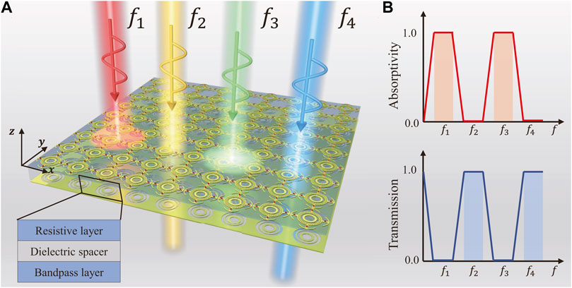
FIGURE 1. Schematic diagram of the cascaded metasurface (A) The cascaded metasurface is composed of a resistive layer, dielectric spacer, and bandpass layer. (B) Absorptivity and transmission characteristics of an ideal dual-band frequency-selective rasorber.
3 Equivalent circuit analysis
Our proposed cascaded metasurface can be analyzed using a two-port equivalent circuit model, as shown in Figure 2. Here, h is the thickness of the dielectric spacer, while
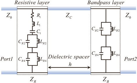
FIGURE 2. Equivalent circuit model of the cascaded metasurface.
According to the equivalent circuit model (ECM) in Figure 2, the transfer matrix (ABCD matrix) can be calculated as:
where,
Moreover, absorption can be calculated by
Hence, we can respectively obtain the impedance conditions for ideal transparency and absorption as:
1) At the transmission band,
2) At the absorption band,
Under the previous two conditions, the design of the EM response for the cascaded metasurface can be incorporated into the design of the equivalent circuit model for the bandpass layer and resistive layer, respectively. For the bandpass layer, it is desirable to exhibit dual-band transmission properties, which are easily achieved by utilizing two cascaded parallel LC circuits with different resonance frequencies
Eq. 4 clearly illustrates that the impedance of the bandpass layer (
In contrast, the resistive layer exhibits two transmission bands at the same frequencies. Here, we employ the RLC series circuit to achieve broadband absorption, but this circuit cannot satisfy the impedance condition (
where,
Based on the previous equivalent circuit model, we can further define the out-of-band absorptive properties. Note that the impedance of the parallel
4 Cascaded metasurface design and analysis
The microstructures of the proposed cascaded metasurface are designed based on previous analysis and using the equivalent circuit model. Figure 3 illustrates the unit-cell geometry of the proposed cascaded metasurface, which consists of a resistor-loaded resistive layer, foam spacer, and dual-bandpass layer as the backplane. This type of unit-cell is periodic along the x- and y-axes, exhibiting a C4 rotational symmetry with an isotropic response. Here, both the resistive layer and the bandpass layer are printed on a 0.508-mm-thick dielectric substrate (F4B-M2) with a permittivity
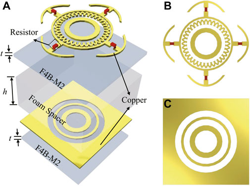
FIGURE 3. Unit-cell geometry of the proposed cascaded metasurface (A) Perspective view of the whole device. (B) Top view of the resistive layer. (C) Top view of the bandpass layer.
To facilitate the design process, we employ the finite-difference time-domain (FDTD) method to compute the scattering properties of the resistive layer and the bandpass layer separately. Then, we adjust the geometry parameters to satisfy the design criteria, i.e.,
A. Bandpass layer
As displayed in the inset of Figure 4, the proposed lossless bandpass layer is a metal plate with two circular-shaped apertures, which realizes the series-connected parallel LC circuits (
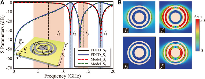
FIGURE 4. Simulation results of the bandpass layer (A) S-parameters of the bandpass layer calculated by full-wave simulation (solid curves) and equivalent circuit model (dashed curves). (B) Surface current distribution on the bandpass layer at the transmission/reflection peaks.
To further illustrate the working principle of the proposed structures, we analyze the mode distributions (surface current) at the frequency of optimal transmission and reflection peaks (7 GHz, 11.5 GHz, 14 GHz, and 17.5 GHz), as shown in Figure 4B. At resonance frequencies of 11.5 and 17.5 GHz, a strong current is excited along with the slot, so the incident waves pass through the slots with low insertion loss. As a result, the impedance of the bandpass layer tends to infinity at transparent frequencies of 11.5 and 17.5 GHz. However, at other frequencies, a very low surface current is induced, indicating that the tangential electric field is extremely weak on the surface of the bandpass layer. The bandpass layer becomes a ground plane and reflects almost all incident waves, indicating that the impedance of the bandpass layer approaches zero at absorptive frequencies of 7 and 14 GHz. Simulation results confirm that the proposed bandpass layer successfully realizes the design of a circuit model with two transmission bands.
B. Resistive layer
Figure 3C presents the geometry of the resistive layer. Here, a complex cross-anchor metallic structure loaded with lumped resistors as well as a metallic loop in the center is employed as the unit element. In addition, the geometry parameters are as follows:
Figure 5A shows the simulated transmission and reflection of the resistive layer under normal incidence waves with TE polarization. There are two transmission bands with an insertion loss of around 0.5 dB at the same frequencies as the transmission bands of the resistive layer (
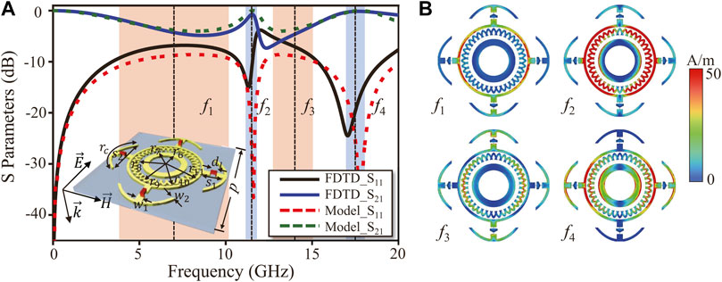
FIGURE 5. Simulation results of the resistive layer (A) S-parameters of the resistive layer calculated by full-wave simulation (solid curves) and equivalent circuit model (dashed curves). (B) Surface current distribution on the resistive layer.
To offer physical insight into the operating principles of the resistive layer, we apply a mode analysis of the surface current distributions on the resistive surface under normal incidence, as demonstrated in Figure 5B. At transmission frequencies of 11.5 and 17.5 GHz, two current paths on the metallic loop are induced. The mode nodes of these current paths are almost fixed and exist in the positions where the lumped resistors are placed. It can be seen that the surface currents are concentrated on the metallic loop resonators. Therefore, no current passes through the lumped resistors and most of the incident waves tunnel through the resistive surface with low insertion loss. As a result, the impedance of the resistive layer tends to infinity at the frequencies with the transmission bands (
5 Experimental characterizations
To further demonstrate the validity of the proposed design, a prototype of the cascaded metasurface is fabricated shown in Figure 6A. The overall size of the assembled prototype is
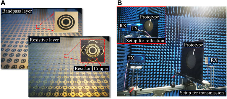
FIGURE 6. Fabricated prototype and the measurement system (A) Photograph of the prototype. (B) Prototype in the measurement setup with the normal incident waves.
Figure 6B illustrates the microwave experimental setup. The prototype is measured in a microwave anechoic chamber using a free-space measurement method. The prototype is placed in the middle of the platform and two standard horn antennas (HD-2040HA15N, HD-4080HA15N, HD-80180HA20N) consisting of a transmitting antenna (TX) and a receiving antenna (RX) are aimed at the prototype. To eliminate the finite size effect caused by prototype edges, we place microwave-absorbing materials around the fabricated sample. Figure 7 shows the experimental and simulated results of EM waves under normal incidence (The equivalent circuit analysis sees Supplementary Material Section S5). As Figure 7A indicates, the measured insertion loss is 0.56 dB at 11.5 GHz and 0.52 dB at 17.5 GHz. Besides, Figure 7B shows that the absorption band with an absorptivity of higher than 80% covers the bands at 3.9–10.2 GHz and 13–15 GHz. The experimental results generally agree with the simulated results, but slight differences mainly originate from fabrication tolerance.
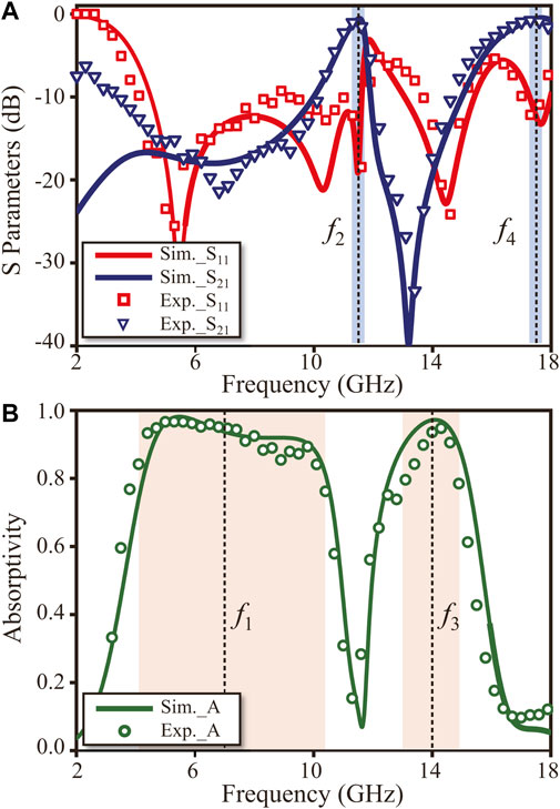
FIGURE 7. Experimental spectra (open symbols) and numerical spectra (solid curves) of the fabricated prototype with (A) transmission/reflection (blue/red), and (B) absorptivity (green).
To further verify the angular robustness and polarization insensitivity of the proposed cascaded metasurface, we simulate the transmissive/absorptive performance under different polarizations and incident angles. Although the high-frequency passband gradually narrows as the incident angle increases, Figures 8A,B reveal that the transmission peaks of the two different polarizations are generally stable at about 11.5 and 17.5 GHz. This is because the transmission peak of the cascaded metasurface is mainly determined by the parallel resonance of the LC, which is stable regardless of the oblique incident angle. Figures 8C,D verifies that our cascaded metasurface has wideband absorption performance. In the range of 4.6–10.2 GHz and 13–15 GHz, the absorption rate of the cascaded metasurface at different polarizations of oblique incidence angles up to 30° is higher than 80% (The results for incident angles larger than 30° are shown in Supplementary Material Section S2).
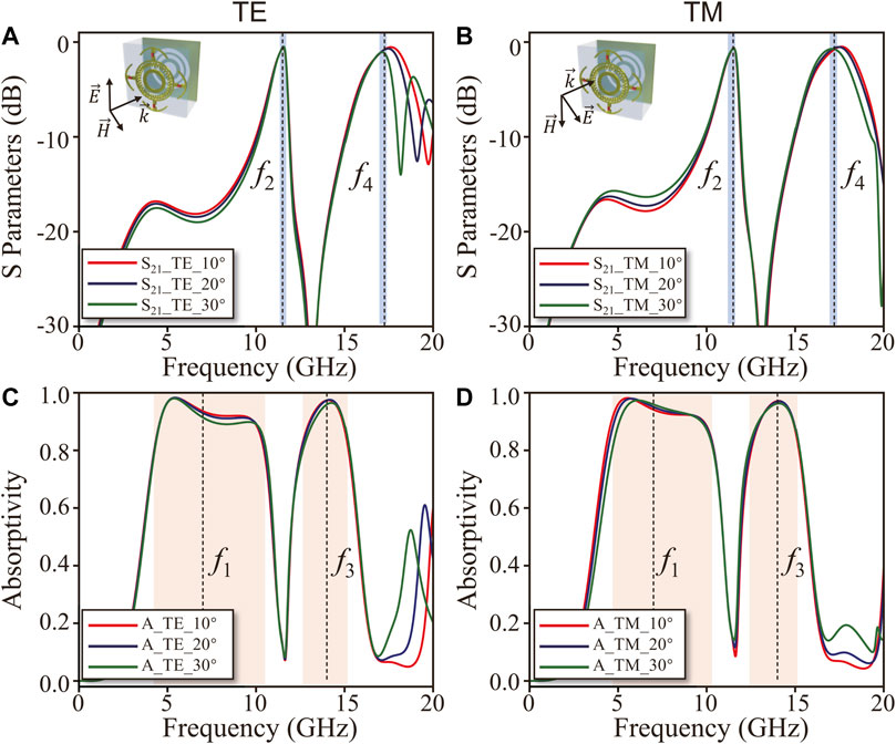
FIGURE 8. Oblique-angle dependence of cascaded metasurface. Transmission coefficients and absorptivity under (A,C) TE polarization, (B,D) TM polarization.
In Table 1, we compare the performance of our design with that of several similar designs reported in previous literature, regarding transmission frequency, insertion loss, absorption bandwidth (with
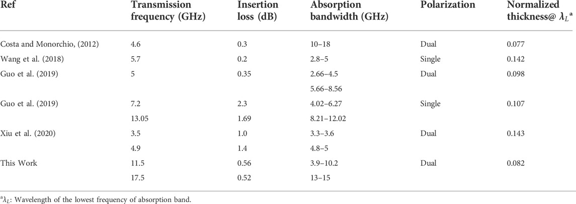
TABLE 1. Performance comparison.
6 Conclusion
In this article , we propose a cascaded metasurface with two transmission bands and two wide absorption bands. The two transmission bands with low insertion loss are realized by connecting a series RLC circuit cascaded with a parallel LC circuit in the resistive layer and properly designing the lossless bandpass. In addition, our present metasurface can be flexibly designed to the desired frequency (other designs see Supplementary Material Section S6). However, we need to note that limitation exists in such a multi-band structure. Once the size of the unit cell has been determined, the total bandwidth is fixed, although the bandwidth ratio per band and the center frequency could be further fine-tuned by adjusting the structure (Guo et al., 2018; Yang et al., 2019). The prototype is fabricated using printed circuit board technology to verify the design method. The experimental measurements exhibit consistency with simulated results. Moreover, the proposed cascaded metasurface has a stable performance concerning polarization and incident angles of EM waves. The cascaded metasurface possesses great potential for communication and radar applications such as antenna radomes, thereby improving the communication security and low observability of platforms.
Data availability statement
The raw data supporting the conclusions of this article will be made available by the authors, without undue reservation.
Author contributions
All authors listed have made a substantial, direct, and intellectual contribution to the work and approved it for publication.
Funding
This work was financially supported by the National Natural Science Foundation of China (Grant Nos. 62175141), the Shanghai Science and Technology Committee (Grant Nos. 20JC1414602), the Shanghai East Scholar Plan, and the Open Fund of State Key Laboratory of Information Photonics and Optical Communications (Beijing University of Posts and Telecommunications, IPOC 2020A002).
Conflict of interest
The authors declare that the research was conducted in the absence of any commercial or financial relationships that could be construed as a potential conflict of interest.
Publisher’s note
All claims expressed in this article are solely those of the authors and do not necessarily represent those of their affiliated organizations, or those of the publisher, the editors, and the reviewers. Any product that may be evaluated in this article, or claim that may be made by its manufacturer, is not guaranteed or endorsed by the publisher.
Supplementary material
The Supplementary Material for this article can be found online at: https://www.frontiersin.org/articles/10.3389/fmats.2022.949076/full#supplementary-material
References
Akram, M. R., Ding, G. W., Chen, K., Feng, Y. J., and Zhu, W. R. (2020). Ultrathin single layer metasurfaces with ultra‐wideband operation for both transmission and reflection. Adv. Mat. 32, 1907308. doi:10.1002/adma.201907308
Arbabi, A., Arbabi, E., Horie, Y., Kamali, S. M., and Faraon, A. (2017). Planar metasurface retroreflector. Nat. Photonics 11, 415–420. doi:10.1038/nphoton.2017.96
Bilgic, M. M., and Yegin, K. (2014). Wideband offset slot-coupled patch antenna array for X/Ku-Band multimode radars. IEEE Antennas Wirel. Propag. Lett. 13, 157–160. doi:10.1109/LAWP.2013.2296911
Cai, B. G., Li, Y. B., Jiang, W. X., Cheng, Q., and Cui, T. J. (2015). Generation of spatial Bessel beams using holographic metasurface. Opt. Express 23, 7593. doi:10.1364/OE.23.007593
Cai, T., Tang, S. W., Zheng, B., Wang, G. M., Ji, W. Y., Qian, C., et al. (2020). Ultrawideband chromatic aberration-free meta-mirrors. Adv. Photonics 3, 016001. doi:10.1117/1.AP.3.1.016001
Cai, X. D., Tang, R., Zhou, H. Y., Li, Q. S., Ma, S. J., Wang, D. Y., et al. (2021). Dynamically controlling terahertz wavefronts with cascaded metasurfaces. Adv. Photonics 3, 036003. doi:10.1117/1.AP.3.3.036003
Cao, Y., Fu, Y. Y., Zhou, Q. J., Ou, X., Gao, L., Chen, H. Y., et al. (2019). Mechanism behind angularly asymmetric diffraction in phase-gradient metasurfaces. Phys. Rev. Appl. 12, 024006. doi:10.1103/PhysRevApplied.12.024006
Chen, Q., Bai, J. J., Chen, L., and Fu, Y. Q. (2015). A miniaturized absorptive frequency selective surface. IEEE Antennas Wirel. Propag. Lett. 14, 80–83. doi:10.1109/LAWP.2014.2355252
Costa, F., and Monorchio, A. (2012). A frequency selective radome with wideband absorbing properties. IEEE Trans. Antennas Propag. 60, 2740–2747. doi:10.1109/TAP.2012.2194640
Guo, H. J., Lin, J., Qiu, M., Tian, J. X., Wang, Q., Li, Y., et al. (2018). Flat optical transparent window: Mechanism and realization based on metasurfaces. J. Phys. D. Appl. Phys. 51, 074001. doi:10.1088/1361-6463/aaa451
Guo, M., Chen, Q., Sun, Z. S., Sang, D., and Fu, Y. Q. (2019). Design of dual-band frequency-selective rasorber. IEEE Antennas Wirel. Propag. Lett. 18, 841–845. doi:10.1109/LAWP.2019.2903336
Guo, M., Lin, Y., Guo, T., Chen, Q., Zheng, Y. J., Fu, Y. Q., et al. (2019). Frequency-selective rasorber with two low insertion loss transmission bands. Int. J. RF Microw. Comput. Aided. Eng. 30, e22044. doi:10.1002/mmce.22044
Guo, Q. X., Li, Z. R., Su, J. X., Yang, L. Y., and Song, J. M. (2019). Dual-polarization absorptive/transmissive frequency selective surface based on tripole elements. IEEE Antennas Wirel. Propag. Lett. 18, 961–965. doi:10.1109/LAWP.2019.2906675
Guo, Q. X., Su, J. X., Li, Z. R., Song, J. M., and Guan, Y. L. (20202020). Miniaturized-element frequency-selective rasorber design using characteristic modes analysis. IEEE Trans. Antennas Propag. 68, 6683–6694. doi:10.1109/TAP.2020.2986640
He, Q., Sun, S. L., Xiao, S. Y., and Zhou, L. (2018). High-efficiency metasurfaces: Principles, realizations, and applications. Adv. Opt. Mat. 6, 1800415. doi:10.1002/adom.201800415
Li, Q. S., Cai, X. D., Liu, T., Jia, M., Wu, Q., Zhou, H. Y., et al. (2022). Gate-tuned graphene meta-devices for dynamically controlling terahertz wavefronts. Nanophotonics 11, 2085–2096. doi:10.1515/nanoph-2021-0801
Ma, H. Y., Kong, X. L., Chen, P., Wang, W. H., Han, K., Zhao, L., et al. (2020). Broadband vortex beams generation with narrow divergence angle using polarization insensitive metasurface. IEEE Access 8, 218062–218068. doi:10.1109/ACCESS.2020.3042236
Mishra, N., Choudhary, D. K., Chowdhury, R., Kumari, K., and Chaudhary, and R. K. (2017). An investigation on compact ultra-thin triple band polarization independent metamaterial absorber for microwave frequency applications. IEEE Access 5, 4370–4376. doi:10.1109/ACCESS.2017.2675439
Parameswaran, A., Kundu, D., and Sonalikar, H. S. (2021). A dual-polarized wideband frequency-selective rasorber with low in-band insertion loss and high oblique incidence stability. IEEE Trans. Electromagn. Compat. 63, 1820–1828. doi:10.1109/TEMC.2021.3072912
Pfeoffer, C., and Grbic, A. (2013). Cascaded metasurfaces for complete phase and polarization control. Appl. Phys. Lett. 102, 231116. doi:10.1063/1.4810873
Ran, J., Xie, M. L., Wen, D. D., Zhang, X. L., and Xue, C. H. (2022). Broadband and dual-polarized terahertz wave anomalous refraction based on a huygens’ metasurface. Front. Mat. 9, 899689. doi:10.3389/fmats.2022.899689
Sharma, A., Malik, S., Ghosh, S., and Srivastava, K. V. (2022). A miniaturized frequency selective rasorber with independently regulated selective dual-transmission response. IEEE Antennas Wirel. Propag. Lett. 21, 257–261. doi:10.1109/LAWP.2021.3127106
Su, T., Yi, X. J., and Wu, B. (2019). X/Ku dual-band single-layer reflectarray antenna. IEEE Antennas Wirel. Propag. Lett. 18, 338–342. doi:10.1109/LAWP.2018.2890766
Sun, S. L., He, Q., Hao, J. M., Xiao, S. Y., and Zhou, L. (2019). Electromagnetic metasurfaces: Physics and applications. Adv. Opt. Photonics 11, 380. doi:10.1364/AOP.11.000380
Sun, S. L., He, Q., Xiao, S. Y., Xu, Q., Li, X., Zhou, L., et al. (2012). Gradient-index meta-surfaces as a bridge linking propagating waves and surface waves. Nat. Mat. 11, 426–431. doi:10.1038/nmat3292
Wang, Z. F., Zeng, Q. S., Fu, J. H., Chen, W., Lv, B., Song, M. X., et al. (2018). A high-transmittance frequency-selective rasorber based on dipole arrays. IEEE Access 6, 31367–31374. doi:10.1109/ACCESS.2018.2843795
Wu, L. W., Xiao, Q., Gou, Y., Wu, R. Y., Xu, P., Qing, Y. M., et al. (2022). Electromagnetic diffusion and encryption holography integration based on reflection–transmission reconfigurable digital coding metasurface. Adv. Opt. Mat. 10, 2102657. doi:10.1002/adom.202102657
Xiao, S. Y., Wang, J. R., Liu, F., Zhang, S., Yin, X. B., Li, J., et al. (2017). Spin-dependent optics with metasurfaces. Nanophotonics 6, 215–234. doi:10.1515/nanoph-2016-0121
Xiao, S. Y., Zhong, F., Liu, H., Zhu, S. N., and Li, J. (2015). Flexible coherent control of plasmonic spin-Hall effect. Nat. Commun. 6, 8360. doi:10.1038/ncomms9360
Xiu, X., Che, W. Q., Yang, W. C., Han, Y., and Xue, Q. (2020). Double-polarized dual-passband Absorptive frequency-selective transmission structure. IEEE Trans. Electromagn. Compat. 62, 1951–1960. doi:10.1109/TEMC.2019.2954533
Xu, H. X., Hu, G. W., Wang, Y. Z., Wang, C. H., Wang, M. Z., Wang, S. J., et al. (2021). Polarization-insensitive 3D conformal-skin metasurface cloak. Light. Sci. Appl. 10, 75. doi:10.1038/s41377-021-00507-8
Xu, Y. D., Fu, Y. Y., and Chen, H. Y. (2016). Planar gradient metamaterials. Nat. Rev. Mat. 1, 16067. doi:10.1038/natrevmats.2016.67
Yang, B. W., Liu, T., Guo, H. J., Xiao, S. Y., and Zhou, L. (2019). High-performance meta-devices based on multilayer meta-atoms: Interplay between the number of layers and phase coverage. Sci. Bull. (Beijing). 64, 823–835. doi:10.1016/j.scib.2019.05.028
Yang, H. H., Yang, F., Cao, X. Y., Xu, S. H., Gao, J., Chen, X. B., et al. (2017). A 1600-element dual-frequency electronically reconfigurable reflectarray at X/Ku-Band. IEEE Trans. Antennas Propag. 65, 3024–3032. doi:10.1109/TAP.2017.2694703
Yang, Y. J., Wu, B., Chen, B., and Zhao, Y. T. (2022). Flexible frequency-selective rasorber based on metal-graphene hybrid metamaterial. Opt. Express 30, 6566. doi:10.1364/OE.451898
Yu, N. F., Genevet, P., Kats, M. A., Aieta, F., Tetienne, J., Capasso, F., et al. (2011). Light propagation with phase discontinuities: Generalized laws of reflection and refraction. Science 334, 333–337. doi:10.1126/science.1210713
Yu, Y. F., Shen, Z. X., Deng, T. W., and Luo, G. Q. (2017). 3-D frequency-selective rasorber with wide upper absorption band. IEEE Trans. Antennas Propag. 65, 4363–4367. doi:10.1109/TAP.2017.2712812
Zhang, H. F., Zhang, X. Q., Xu, Q., Tian, C. X., Wang, Q., Xu, Y. H., et al. (2017). High-efficiency dielectric metasurfaces for polarization-dependent terahertz wavefront manipulation. Adv. Opt. Mat. 6, 1700773. doi:10.1002/adom.201700773
Zhen, Z., Qian, C., Jia, Y. T., Fan, Z. X., Hao, R., Cai, T., et al. (2021). Realizing transmitted metasurface cloak by a tandem neural network. Photonics Res. 9, B229. doi:10.1364/PRJ.418445
Keywords: frequency-selective rasorber, metasurfaces, metamaterials, equivalent circuit model, parallel resonance
Citation: Li Q, Li X, Chen Y, Ding F, Chen C, Liu H and Xiao S (2022) High-performance dual-band frequency-selective rasorber based on cascaded metasurface. Front. Mater. 9:949076. doi: 10.3389/fmats.2022.949076
Received: 20 May 2022; Accepted: 28 June 2022;
Published: 25 July 2022.
Edited by:
Yifan Zhu, Southeast University, ChinaReviewed by:
Ke Chen, Nanjing University, ChinaNaveen Mishra, VIT University, India
Teng Li, Southeast University, China
Copyright © 2022 Li, Li, Chen, Ding, Chen, Liu and Xiao. This is an open-access article distributed under the terms of the Creative Commons Attribution License (CC BY). The use, distribution or reproduction in other forums is permitted, provided the original author(s) and the copyright owner(s) are credited and that the original publication in this journal is cited, in accordance with accepted academic practice. No use, distribution or reproduction is permitted which does not comply with these terms.
*Correspondence: Shiyi Xiao, cGh4aWFvQHNodS5lZHUuY24=; Huanhuan Liu, bGl1aGhAc3VzdGVjaC5lZHUuY24=
†These authors contributed equally to this work