 Likun Ai
 Fangkun Tian1,2
- 1Key Laboratory of Terahertz Solid State Technology, Shanghai Institute of Microsystem and Information Technology, Chinese Academy of Sciences, Shanghai, China
- 2Center of Materials Science and Optoelectronics Engineering, University of Chinese Academy of Sciences, Beijing, China
In this paper, The InxAl1-xAs graded buffer was inserted between the InAlAs buffer layer and the pseudomorphic In0.66Ga0.34As channel layer to improve material quality in channel. The results show that the InxAl1-xAs graded buffer layer with 50 nm thickness can obtain a good heterojunction interface and the root mean square (RMS) of 0.154 nm. The two dimensional electron gas (2-deg) mobility and concentration were 8570 cm2/Vs. and 2.7 cm−2 × 1012 cm−2 at 300K, respectively. InxAl1-xAs graded buffer layer can enhance the interface quality and the electrical performance through releasing the interface strain caused by pseudomorphic In0.52Al0.48As/In0.66Ga0.34As HEMT. This study shows great potentials by incorporating InxAl1-xAs graded buffer layer in pseudomorphic InP HEMT materials to improve the properties of devices.
Introduction
InP based In0.52Al0.48As/InyGa1-yAs (y > 0.53) pseudomorphic high-electron mobility transistors (PHEMTs) are promising millimeter wave and terahertz wave devices, because of their high superior frequency, low power consumption and low noise characteristics (Schleeh et al., 2012; Fatah et al., 2015; Ajayan and Nirmal, 2017; Takahashi et al., 2017; Ajayan et al., 2018). InP PHEMTs with high mobility, high electron saturation velocity, reasonable bandgap and low electron effective mass are widely applied in the fields of satellite communication, collision avoidance radars, space satellite receivers, monolithic microwave integrated circuits (MMIC) and terahertz monolithic integrated circuits (TMIC) amplifiers etc. (Ai et al., 2017; Ajayan et al., 2020; Hamza et al., 2021).
From the material perspective, the most effective and the simplest way to improve the performance of HEMT materials is to increase the channel indium components. Because its results in reduced the width of the band gap and enhanced mobility of electrons in the channel (Takahashi et al., 2008; Ajayan and Nirmal, 2015; Shi et al., 2015; Tong et al., 2020; Zhong et al., 2020; Feng et al., 2022). However, the lattice mismatch between the pseudomorphic InyGa1-yAs channel and the InAlAs buffer will occur. Dislocation defects, 3D islands and rough interface will lead to the decline in mobility (Lee et al., 1996; Arai et al., 2009; Gu et al., 2012). Various dislocation restriction methods has been applied to reduce the interface defects, such as graded buffer, strain-compensated supper lattice, well-distributed thickness buffer, dilute nitride buffers, multiple layers of self-organized quantum dots, two-step growth technique, metamorphic lattice-mismatched growth etc. (Hudait et al., 2009; Kirch et al., 2010; Gu et al., 2011). The graded buffer layer was proved beneficial for the full relaxation of residual strain.
In the study, the InP HEMT structures with and without InxAl1-xAs graded buffer were designed. The InxAl1-xAs graded buffer was inserted between the InAlAs buffer layer and the pseudomorphic InyGa1-yAs channel layer to solve the problem of lattice mismatch. Epitaxial layer structures of InP PHEMTs were grown on a semi-insulating InP substrate by gas source molecular beam epitaxy (GSMBE). The lattice mismatch of the InxAl1-xAs and InyGa1-yAs epilayers to InP substrate were measured by high-resolution X-ray diffraction (HRXRD). The electron mobility, surface roughness and thickness of materials were measured by Hall measurements, atomic force microscope (AFM) and step profiler, respectively.
Experimental procedure
The InP PHEMT materials were grown by the VG Semicon V90 GSMBE. The elemental aluminum (Al), gallium (Ga), and indium (In) sources were used as group III sources. The silicon (Si) was used as n-type doping source. Their fluxes were controlled by adjusting the cell temperatures, respectively. Phosphine (PH3) and Arsine (AsH3) were used as group V sources. The cracking temperatures were about 1,000°C, and fluxes were controlled by adjusting the pressure. InxAl1-xAs graded buffer layer was designed grading through decrease in aluminum source temperature. The growth rates of InP, InAlAs and InGaAs were 0.5 μm/h, 1 μm/h and 1 μm/h, respectively.
Figure 1 shows the material structure of InP based PHEMTs. The epitaxial layers from bottom to top consist of a semi-insulating InP substrate over which a (500-z)nm thickness In0.52Al0.48As buffer layer was employed. Above the buffer layer a (500-z) thickness InxAl1-xAs graded buffer layer was placed. The 10 nm thickness InyGa1-yAs channel layer was grown. The thickness of the In0.52Al0.48As spacer layer was 3 nm. A Si-δ doping layer with a doping concentration of 5 cm−2 × 1012 cm−2 was placed above the upper In0.52Al0.48As spacer layer, over which a 8 nm In0.52Al0.48As barrier layer and 4 nm InP etch-stop layer were placed, respectively. An n-type In0.52Al0.48As cap layer of 15 nm thickness and n-type In0.65Ga0.35As cap layer of a 25 nm thickness were grown on the top layer.
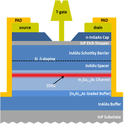
FIGURE 1. InP PHEMT material structure with and without InxAl1-xAs graded buffer.
The lattice mismatch of the InGaAs and In1-yGayAs1-xBix epilayers to InP substrate were measured by high-resolution X-ray diffraction (HRXRD).
Results and discussion
For investigating high mismatch InGaAs channel materials, the InGaAs channel materials with 64, 66, 68, 70% of the indium contents were designed. The design is because 64% of the indium contents has a large mismatch with InP substrate and 70% of the indium is almost the highest contents with a good 2-deg properties in reported previously (Ajayan and Nirmal, 2015; Zhong et al., 2020).
Firstly, the effect of different indium contents of InyGa1-yAs channel on the 2-deg properties of HEMT materials without InxAl1-xAs graded buffer layer were investigated as shown in Table 1. It can be seen from Figure 2 hall data, the increasing mobility with the channel indium contents increases first and then decreases at 300K (77K). The highest mobility was 8020cm2/v·s (24000cm2/v·s), and the surface density was 2.735 cm2 × 1012 cm2 (2.366 cm2 × 1012 cm2), when the indium content was 66%. Because increasing the indium contents of the InyGa1-yAs channel can reduce the gapband width and imprison more electrons for higher mobility. However, when indium contents increases to a certain extent, the lattice constant of the InyGa1-yAs channel material becomes large and the InAlAs barrier tends to mismatch to produce the interface strain. The interface rough scattering can lead to the reduced mobility. Experimental results show that 66% of the indium contents was the best. Alloy disordered scattering can lead to the reduced mobility when indium content was 68%. In the ternary III-V semiconductor alloy InxGa1−xAs, the alloy disorder at and near the interface arising due to chemical intermixing gives a significant contribution to the electron scattering. For well layers made of a ternary alloy, the alloy disorder scattering in the well is shown to yield a dominant contribution to electron scattering (Ogale and Madhukar, 1984). The semiempirical expression model describing the effects of alloy scattering can be expressed as
Where
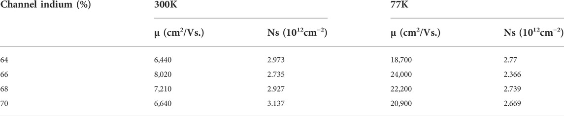
TABLE 1. The 2-deg properties with different channel indium contents at 300K (77K).
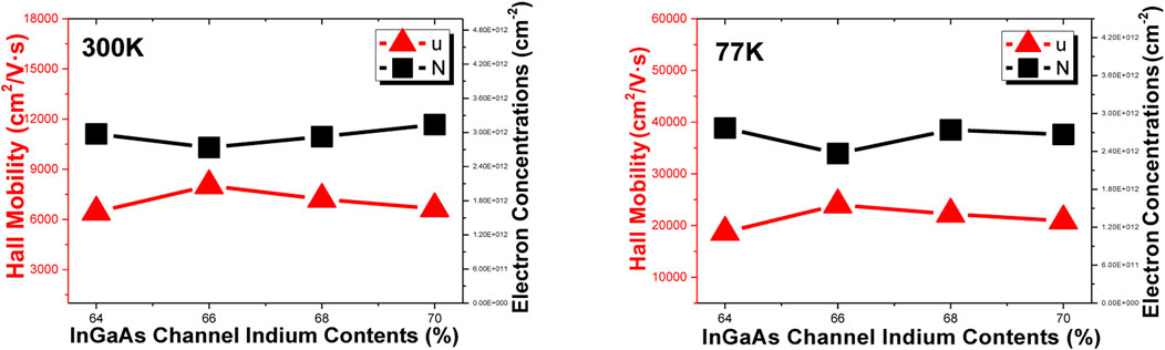
FIGURE 2. The 2-deg properties with different channel indium contents at 300K (77K).
As shown in Figure 3, HRXRD swing curve and atomic force microscope (AFM) images. The indium content of 66%, gallium content of 34%, the mismatch of 4,443, the full-width-at-half-maximum (FWHM) of 48.8s in the In0.66Ga0.34As epitaxial peak were achieved. The root mean square roughness (RMS) was 0.212nm, and the surface was smooth. The indium content of 71%, gallium content of 29%, the mismatch of 5,656, FWHM of 96.55s, RMS of 1.02 nm in the In0.7Ga0.3As epitaxial peak were achieved. It can be seen from the AFM image, the strain had occurred on the material surface.
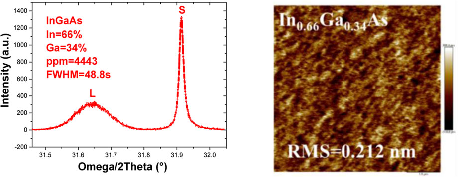
FIGURE 3. The HRXRD swing curve and the AFM images of In0.66Ga0.34As.
Secondly, the effect of six groups InxAl1-xAs graded buffer layers on the HEMT materials with InxAl1-xAs graded buffer layer were investigated. Figure 4 shows the performance of six groups InxAl1-xAs graded buffer layers with different thicknesses which were 0 nm (without buffer layer), 10, 30, 50, 70 and 90 nm, respectively. The indium contents of InxAl1-xAs was graded from 52 to 62%. AFM tapping mode on 5 µm2 × 5 µm2 area was used to characterize the surface morphology of the InxAl1-xAs graded buffer layer with different thicknesses as shown in Figure 4. The sample that graded buffer layer of 0 nm had a minimum RMS of 0.117nm, and the surface quality was significantly better than the other samples. Because the InAlAs and InP substrate lattice match. As the thickness of the InxAl1-xAs graded buffer layer increased, the RMS tended to decrease first and then increase. The best RMS was 0.154 nm when the thickness was 50 nm. The InxAl1-xAs grade buffer layer surface had great fluctuation due to interface strain when the thickness was 90 nm.
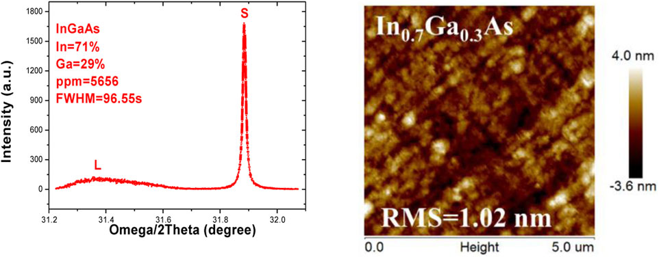
FIGURE 4. AFM images of InxAl1-xAs graded buffer layer with different thickness.
The In0.66Ga0.34As and In0.7Ga0.3As channel materials which grown on 50 nm InxAl1-xAs graded buffer layer were investigated. HRXRD swing curve and AFM images were shown in Figures 5, 6. From the XRD image of In0.66Ga0.34As epitaxial peak, indium content of 66%, gallium content of 34%, mismatch of 4,363, FWHM of t 43.6s and the RMS of 0.212 nm were achieved. In Figure 6, indium content of 70%, gallium content of 30%, mismatch of 5,301, FWHM of 56.9 s and RMS of 1.02 nm were achieved in the InGaAs epitaxial peak. Contrast to Figures 3, 7, the In0.66Ga0.34As and In0.7Ga0.3As channel materials quality have been significantly improved with the 50 nm InxAl1-xAs graded buffer layer was inserted. The design of InxAl1-xAs graded buffer layer can improve channel materials quality significantly, which shows great potentials to improve the properties of devices in pseudomorphic HEMT.
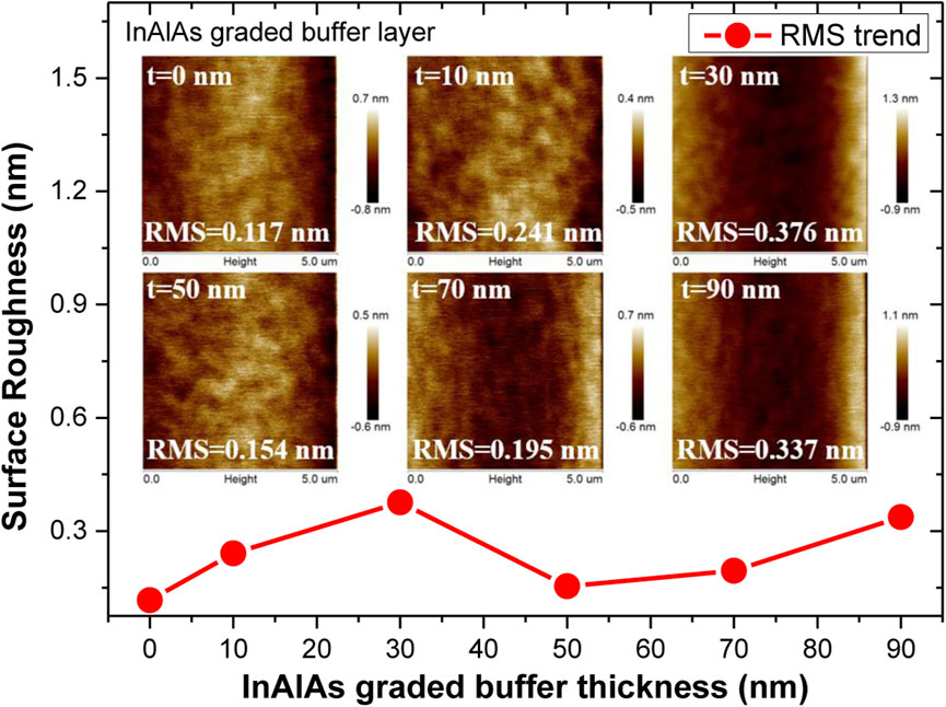
FIGURE 5. The HRXRD swing curve and the AFM images of In0.66Ga0.34As.
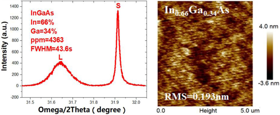
FIGURE 6. The HRXRD swing curve and the AFM images of In0.7Ga0.3As.
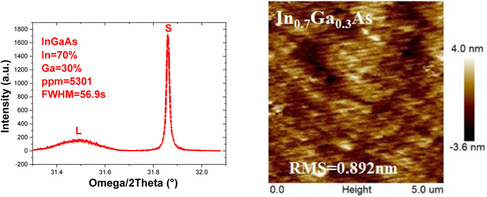
FIGURE 7. The HRXRD swing curve and the AFM images of In0.7Ga0.3As.
Hall characterizations of the In0.66Ga0.34As channel HEMT with the InxAl1-xAs graded buffer layers from 0 to 90 nm thickness were investigated. Hall characterization of the experimental samples as shown in Table 2 and Figure 8. The highest 2-deg mobility of 8570cm2/(v·s) and best RMS of 0.154 nm were achieved when the buffer is 50 nm. It can be showed that the design of 50 nm InxAl1-xAs graded buffer layer can enhance the interface quality and the electrical performance through releasing the interface strain.
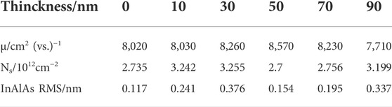
TABLE 2. The performance of the different InxAl1-xAs graded buffer layers with In0.66Ga0.34As channel.
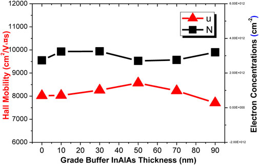
FIGURE 8. The 2-deg properties of different InxAl1-xAs graded buffer layers with In0.66Ga0.34As channel.
Figure 9 shows the TEM image of InP PHEMT material structure with 50 nm thickness InxAl1-xAs graded buffer layer. It can be seen that good channel material surface and material interface qualities were achieved.
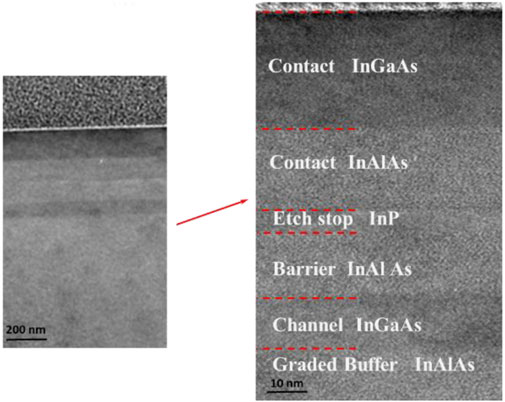
FIGURE 9. The TEM image of In0.66Ga0.34As channel PHEMT with 50 nm InxAl1-xAs graded buffer layer.
Conclusion
In the study, the pseudomorphic In0.52Al0.48As/In0.66Ga0.34As HEMT structures with and without InxAl1-xAs graded buffer were designed and grown. The InxAl1-xAs graded buffer was inserted between the InAlAs buffer layer and the pseudomorphic InyGa1-yAs channel layer to solve the problem of lattice mismatch. The results show that the InxAl1-xAs graded buffer layer with 50 nm thickness can obtain a good heterojunction interface and the root mean square (RMS) of 0.154 nm. The two dimensional electron gas (2-deg) mobility and concentration were 8570 cm2/Vs. and 2.7cm−2 × 1012 cm−2 at 300K, respectively. InxAl1-xAs graded buffer layer can enhance the interface quality and the electrical performance through releasing the interface strain. This study shows great potentials by incorporating InxAl1-xAs graded buffer layer in pseudomorphic HEMT materials to improve the properties of materials.
Data availability statement
The original contributions presented in the study are included in the article/supplementary material, further inquiries can be directed to the corresponding author.
Author contributions
Material growth and test analysis by LA, FT, and HH materials structure designed by AX and MQ.
Conflict of interest
The authors declare that the research was conducted in the absence of any commercial or financial relationships that could be construed as a potential conflict of interest.
Publisher’s note
All claims expressed in this article are solely those of the authors and do not necessarily represent those of their affiliated organizations, or those of the publisher, the editors and the reviewers. Any product that may be evaluated in this article, or claim that may be made by its manufacturer, is not guaranteed or endorsed by the publisher.
References
Ai, L., Zhou, S., Qi, M., Xu, A., and Wang, S. (2017). InGaAsBi materials grown by gas source molecular beam epitaxy. J. Cryst. Growth, InGaAsBi Mater. grown by gas source Mol. beam epitaxyJournal Cryst. Growth 477, 135–138. doi:10.1016/j.jcrysgro.2017.03.011
Ajayan, J., and Nirmal, D. (2017). 22nm In0.75Ga0.25As channel-based HEMTs on InP/GaAs substrates for future THz applications. J. Semicond. 38, 27–32. doi:10.1088/1674-4926/38/4/044001
Ajayan, J., and Nirmal, D. (2015). A review of InP/InAlAs/InGaAs based transistors for high frequency applications. Superlattices Microstruct. 86, 1–19. doi:10.1016/j.spmi.2015.06.048
Ajayan, J., Nirmal, D., Mohankumar, P., and Arivazhagan, L. (2020). Investigation of impact of passivation materials on the DC/RF performances of InP-HEMTs for terahertz sensing and imaging. Silicon 12, 1225–1230. doi:10.1007/s12633-019-00226-1
Ajayan, J., Ravichandran, T., Mohankumar, P., Prajoon, P., Charles Pravin, J. C., and Nirmal, D. (2018). Investigation of DC-RF and breakdown behaviour in L g = 20 nm novel asymmetric GaAs MHEMTs for future submillimetre wave applications. AEU - Int. J. Electron. Commun. 84, 387–393. doi:10.1016/j.aeue.2017.12.022
Arai, M., Tadokoro, T., Fujisawa, T., Kobayashi, W., Nakashima, K., Yuda, M., et al. (2009). Uncooled (25-85° C) 10 Gbit/s operation of 1.3µm-range metamorphic Fabry-Perot laser on GaAs substrate. Electron. Lett. 45, 1. doi:10.1049/el.2009.0263
Bellotti, Enrico, and Goano, FrancescoM. (2007). Alloy scattering in AlGaN and InGaN: A numerical study. J. Appl. Phys. 101, 123706. doi:10.1063/1.2748353
Fatah, F. A., Lin, Y.-C., Lee, T.-Y., Yang, K.-C., Liu, R.-X., Chan, J.-R., et al. (2015). Potential of enhancement mode In0.65Ga0.35As/InAs/in0.65Ga0.35As HEMTs for using in high-speed and low-power logic applications. ECS J. Solid State Sci. Technol. 4, N157–N159. doi:10.1149/2.0171512jss
Feng, R., Wang, B., Cao, S., Liu, T., Su, Y., Ding, W., et al. (2022). Impact of symmetric gate-recess length on the DC and RF characteristics of InP HEMTs. Chin. Phys. B 31, 18505–018505. doi:10.1088/1674-1056/ac364d
Gu, Y., Zhang, Y., Wang, K., Fang, X., Li, C., Cao, Y., et al. (2011). InP-based InAs/InGaAs quantum wells with type-I emission beyond 3 μm. Appl. Phys. Lett. 99, 081914. doi:10.1063/1.3629999
Gu, Y., Zhang, Y., Wang, K., Fang, X., and Liu, K. (2012). InAlAs graded metamorphic buffer with digital alloy intermediate layers. Jpn. J. Appl. Phys. 51, 080205. doi:10.1143/jjap.51.080205
Hamza, K. H., Nirmal, D., Fletcher, A. A., Arivazhagan, L., Ajayan, J., and Natarajan, R. (2021). Highly scaled graded channel GaN HEMT with peak drain current of 2.48 A/mm. AEU-International J. Electron. Commun. 136, 153774.
Hudait, M. K., Lin, Y., and Ringel, S. (2009). Strain relaxation properties of InAsyP1−y metamorphic materials grown on InP substrates. J. Appl. Phys. 105, 061643. doi:10.1063/1.3098232
Kirch, J., Garrod, T., Kim, S., Park, J. H., Shin, J. C., Mawst, L., et al. (2010). InAsyP1−y metamorphic buffer layers on InP substrates for mid-IR diode lasers. J. Cryst. growth 312, 1165–1169. doi:10.1016/j.jcrysgro.2009.12.057
Lee, B., Baek, J., Lee, J., Choi, S., Jung, S., Han, W., et al. (1996). Optical properties of InGaAs linear graded buffer layers on GaAs grown by metalorganic chemical vapor deposition. Appl. Phys. Lett. 68, 2973–2975. doi:10.1063/1.116373
Ogale, S. B., and Madhukar, A. (1984). Alloy disorder scattering contribution to low‐temperature electron mobility in semiconductor quantum well structures. J. Appl. Phys. 56, 368–374. doi:10.1063/1.333974
Schleeh, J., Alestig, G., Halonen, J., Malmros, A., Nilsson, B., Nilsson, P., et al. (2012). Ultralow-power cryogenic InP HEMT with minimum noise temperature of 1 K at 6 GHz. IEEE Electron Device Lett. 33, 664–666. doi:10.1109/led.2012.2187422
Shi, L., Feng, S., Liu, K., and Zhang, Y. (2015). Mechanism of the self-changing parameters and characteristics in AlGaN/GaN high-electron mobility transistors after a step voltage stress. J. Semicond. 36, 074005. doi:10.1088/1674-4926/36/7/074005
Takahashi, T., Kawano, Y., Makiyama, K., Shiba, S., Sato, M., Nakasha, Y., et al. (2017). Maximum frequency of oscillation of 1.3 THz obtained by using an extended drain-side recess structure in 75-nm-gate InAlAs/InGaAs high-electron-mobility transistors. Appl. Phys. Express 10, 024102. doi:10.7567/apex.10.024102
Takahashi, T., Makiyama, K., Hara, N., Sato, M., and Hirose, T. (2008). “Improvement in high frequency and noise characteristics of InP-based HEMTs by reducing parasitic capacitance,” in 2008 20th international conference on indium phosphide and related materials (IEEE), 1–4. doi:10.1109/iciprm.2008.4702964
Tong, Z. H., Ding, P., Su, Y. B., Wang, D. H., and Jin, Z. (2020). Impacts of increasing gate stem height on DC and RF performances of InAlAs/InGaAs InP based HEMTs. Chin. Phys. B 30.
Keywords: INP, pHEMT, InxAl1-xAs, graded buffer layer, pseudomorphic
Citation: Ai L, Tian F, Xu A, Huang H and Qi M (2022) Effect of InxAl1-xAs graded buffer materials on pseudomorphic InP HEMT. Front. Mater. 9:980077. doi: 10.3389/fmats.2022.980077
Received: 28 June 2022; Accepted: 29 July 2022;
Published: 25 August 2022.
Edited by:
Robert Richards, The University of Sheffield, United KingdomReviewed by:
Ankit Kumar Pandey, Bennett University, IndiaMeryleen Mohapatra, Siksha O Anusandhan University, India
Copyright © 2022 Ai, Tian, Xu, Huang and Qi. This is an open-access article distributed under the terms of the Creative Commons Attribution License (CC BY). The use, distribution or reproduction in other forums is permitted, provided the original author(s) and the copyright owner(s) are credited and that the original publication in this journal is cited, in accordance with accepted academic practice. No use, distribution or reproduction is permitted which does not comply with these terms.
*Correspondence: Likun Ai, bGlrdW5haUBtYWlsLnNpbS5hYy5jbg==